EP0527033B1 - Halbleitermodul - Google Patents
Halbleitermodul Download PDFInfo
- Publication number
- EP0527033B1 EP0527033B1 EP92307117A EP92307117A EP0527033B1 EP 0527033 B1 EP0527033 B1 EP 0527033B1 EP 92307117 A EP92307117 A EP 92307117A EP 92307117 A EP92307117 A EP 92307117A EP 0527033 B1 EP0527033 B1 EP 0527033B1
- Authority
- EP
- European Patent Office
- Prior art keywords
- conductor
- electrode
- pair
- semiconductor
- conductors
- Prior art date
- Legal status (The legal status is an assumption and is not a legal conclusion. Google has not performed a legal analysis and makes no representation as to the accuracy of the status listed.)
- Expired - Lifetime
Links
Images


Classifications
-
- H—ELECTRICITY
- H10—SEMICONDUCTOR DEVICES; ELECTRIC SOLID-STATE DEVICES NOT OTHERWISE PROVIDED FOR
- H10W—GENERIC PACKAGES, INTERCONNECTIONS, CONNECTORS OR OTHER CONSTRUCTIONAL DETAILS OF DEVICES COVERED BY CLASS H10
- H10W72/00—Interconnections or connectors in packages
-
- H—ELECTRICITY
- H10—SEMICONDUCTOR DEVICES; ELECTRIC SOLID-STATE DEVICES NOT OTHERWISE PROVIDED FOR
- H10W—GENERIC PACKAGES, INTERCONNECTIONS, CONNECTORS OR OTHER CONSTRUCTIONAL DETAILS OF DEVICES COVERED BY CLASS H10
- H10W44/00—Electrical arrangements for controlling or matching impedance
- H10W44/501—Inductive arrangements
-
- H—ELECTRICITY
- H10—SEMICONDUCTOR DEVICES; ELECTRIC SOLID-STATE DEVICES NOT OTHERWISE PROVIDED FOR
- H10W—GENERIC PACKAGES, INTERCONNECTIONS, CONNECTORS OR OTHER CONSTRUCTIONAL DETAILS OF DEVICES COVERED BY CLASS H10
- H10W70/00—Package substrates; Interposers; Redistribution layers [RDL]
- H10W70/40—Leadframes
- H10W70/481—Leadframes for devices being provided for in groups H10D8/00 - H10D48/00
-
- H—ELECTRICITY
- H10—SEMICONDUCTOR DEVICES; ELECTRIC SOLID-STATE DEVICES NOT OTHERWISE PROVIDED FOR
- H10W—GENERIC PACKAGES, INTERCONNECTIONS, CONNECTORS OR OTHER CONSTRUCTIONAL DETAILS OF DEVICES COVERED BY CLASS H10
- H10W90/00—Package configurations
-
- H—ELECTRICITY
- H10—SEMICONDUCTOR DEVICES; ELECTRIC SOLID-STATE DEVICES NOT OTHERWISE PROVIDED FOR
- H10W—GENERIC PACKAGES, INTERCONNECTIONS, CONNECTORS OR OTHER CONSTRUCTIONAL DETAILS OF DEVICES COVERED BY CLASS H10
- H10W90/00—Package configurations
- H10W90/701—Package configurations characterised by the relative positions of pads or connectors relative to package parts
-
- H—ELECTRICITY
- H10—SEMICONDUCTOR DEVICES; ELECTRIC SOLID-STATE DEVICES NOT OTHERWISE PROVIDED FOR
- H10W—GENERIC PACKAGES, INTERCONNECTIONS, CONNECTORS OR OTHER CONSTRUCTIONAL DETAILS OF DEVICES COVERED BY CLASS H10
- H10W72/00—Interconnections or connectors in packages
- H10W72/50—Bond wires
- H10W72/541—Dispositions of bond wires
- H10W72/547—Dispositions of multiple bond wires
- H10W72/5475—Dispositions of multiple bond wires multiple bond wires connected to common bond pads at both ends of the wires
-
- H—ELECTRICITY
- H10—SEMICONDUCTOR DEVICES; ELECTRIC SOLID-STATE DEVICES NOT OTHERWISE PROVIDED FOR
- H10W—GENERIC PACKAGES, INTERCONNECTIONS, CONNECTORS OR OTHER CONSTRUCTIONAL DETAILS OF DEVICES COVERED BY CLASS H10
- H10W72/00—Interconnections or connectors in packages
- H10W72/50—Bond wires
- H10W72/551—Materials of bond wires
- H10W72/552—Materials of bond wires comprising metals or metalloids, e.g. silver
- H10W72/5524—Materials of bond wires comprising metals or metalloids, e.g. silver comprising aluminium [Al]
-
- H—ELECTRICITY
- H10—SEMICONDUCTOR DEVICES; ELECTRIC SOLID-STATE DEVICES NOT OTHERWISE PROVIDED FOR
- H10W—GENERIC PACKAGES, INTERCONNECTIONS, CONNECTORS OR OTHER CONSTRUCTIONAL DETAILS OF DEVICES COVERED BY CLASS H10
- H10W90/00—Package configurations
- H10W90/701—Package configurations characterised by the relative positions of pads or connectors relative to package parts
- H10W90/751—Package configurations characterised by the relative positions of pads or connectors relative to package parts of bond wires
- H10W90/754—Package configurations characterised by the relative positions of pads or connectors relative to package parts of bond wires between a chip and a stacked insulating package substrate, interposer or RDL
Definitions
- the present invention relates to a semiconductor module accommodating a plurality of semiconductor elements fixed on the insulating plates of one container, and having each element connected to the other, as well as to external terminals.
- Modules which comprise a plurality of semiconductor elements such as transistor chips connected with each other and contained in a container with external terminals are used widely as modules for constructing circuits.
- An example of such a module is shown in Figure 3, where the emitter electrode of a first transistor 21 is connected to the collector electrode of a second transistor 22.
- the module has a connecting wire for the terminal E1C2. The wire is drawn out from the common connection of both transistors.
- the module has a structure in which the chip 11 corresponding to the transistor 21 and the chip 12 corresponding to the transistor 22 are fixed onto the collector electrode conductors 31, 32 on the insulating plates 41, 42, the emitter electrodes on the chips 11, 12 are connected to the emitter electrode conductors 33, 34 on the insulating plates 41, 42, respectively, by using the connecting wire 5, and the C1 terminal 61 is connected to the collector electrode conductor 31, the E2 terminal conductor 62 to the emitter electrode conductor 34, and the E1 C2 terminal conductor 63 is connected to the emitter electrode conductor 33 and to the collector electrode conductor 32. Furthermore, the insulating plates 41, 42 are fixed to the container bottom plate 7, and the terminal conductors 61, 62, 63 are drawn to above the container.
- the chip 13 of the transistor 23 is fixed to the electrode conductor 31 on the insulation plate 41 in addition to the chip 11 of the transistor 21, while the chip 14 of the transistor 24 is fixed to the electrode conductor 32 on the insulation plate 42 in addition to the chip 12 of the transistor 22.
- the terminal conductors 61, 62, 63 are drawn out in the similar manner as in Figure 4.
- EP-A-340 466 shows a structure where a bond wire between an electrode of a semiconductor element and its corresponding terminal is provided with a shunt connector of larger current capacity than the bond wire extending from the electrode to the terminal. Should the bond wire fuse due to excessive current loading, failure of the element is prevented by the current passing through the shunt connector.
- the object of the present invention is to provide a semiconductor module with the floating inductance reduced to decrease the surge voltage generated during a change in current, which voltage is due to the floating inductance of conductors connecting elements of a semiconductor module containing a plurality of semiconductor elements in one container.
- the present invention provides a semiconductor module comprising two semiconductor elements each having first and second main electrodes, a first main terminal conductor connected to the first main electrode of the first element by a first electrode conductor and a second main terminal conductor connected to the second main electrode of the second element by a second electrode conductor, and one intermediate terminal conductor is connected to both the second main electrode of the first element and to the first main electrode of the second element by a third electrode conductor and a fourth electrode conductor, characterised in that a shunt conductor is connected, in parallel with the intermediate terminal conductor, between the second main electrode of the first element and the first main electrode of the second element, the shunt conductor having a lower floating inductance and a higher resistance than the part of the intermediate terminal conductor between the second main electrode of the first element and the first main electrode of the second element.
- a semiconductor module characterised in that two or more semiconductor elements are fixed on each first and fourth electrode conductor, whereas connecting conductors with a nearly equivalent floating inductance and resistance are connected to the first electrode conductor of the second element at locations nearly equidistant from each element. It is also effective to construct a semiconductor module characterised in that the connecting conductors are arranged at locations closer to the second electrode conductor of the first element and the first electrode conductor of the second element.
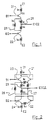
- Figure 1 shows an equivalent circuit of the semiconductor module according to the present invention, in which the semiconductor elements are transistors.
- the same numerals are given to the parts common to those in Figure 3.
- the equivalent circuit is disposed with the shunt conductor 26 connected in parallel to that part of the terminal conductor 25 which lets the main current flow therein from the emitter of the first transistor 21 to the collector of the second transistor 22 and is connected to the E1 C2 terminal conductor.
- the shunt conductor 26 has a high direct current resistance as well as a lower floating inductance I' than the floating inductance I E1 of the terminal conductor 25. As a result, the stationary current flows through the terminal conductor 25 which has a smaller resistance.
- the terminal conductor 25 is brought to have higher alternating current impedance and the current is shunted to the shunt conductor 26, because the floating inductance I E1 is higher than the floating inductance I' in the shunt conductor 26.
- This parallel connection reduces the floating inductance between the emitter of the first transistor 21 and the collector of the second transistor 22, thereby suppressing the surge voltage. Since the time during which the current flows through the shunt conductor is only that time during which the current decreases, a problem such as heat generation due to a voltage drop does not occur even if the direct current resistance is high.
- Figure 2 also shows another equivalent circuit of the semiconductor device according to the present invention, having four transistors as the semiconductor elements, with the parts that are same as those in Figure 5 given the same numerals.
- another shunt conductor 27 is disposed, and is connected in proximity to the first transistor 21, while the shunt conductor 26 is connected in proximity to the third transistor 23.
- the shunt conductor 27 has nearly the same floating inductance I' and resistance as the shunt conductor 26, and therefore, a current of nearly the same magnitude is shunted to both of the shunt conductors 26, 27 when the first and third transistors 21, 23 are turned off, and no surge voltage due to the current through the floating inductance I E1 is generated.
- FIG 7 shows a first embodiment of the present invention, with the parts common to those in Figure 4 given the same reference numerals.
- the electrode conductor 32 is formed so that part of the collector electrode conductor 32 on the insulation plate 42 is located closer to the emitter electrode 33 on the insulation plate 41, and these are connected via an ultrasonic bonding with two thin metallic wires 5 made of the same thin aluminium wire as the leads used to connect the transistor chips 11, 12 to the emitter electrode conductors 33, 32.
- Selecting the thin metallic wire in a manner that ensures that its length is shorter and its floating inductance is smaller than those of the bridge 64 on the E1C2 terminal conductor 63 results in an equivalent circuit as shown in Figure 1.
- the main current flows along a path from C1 to the transistor 21 and then to I E1 and terminal E1 C2.
- I c decreases when the transistor 21 is turned off, a surge voltage ⁇ V of I E1 x dl c /dt is generated as described earlier on the emitter side of the transistor 21 in accordance with the magnitude of dl c /dt and the floating inductance I E1 .
- the current I C is shunted into the current I 1 flowing into I E1 and the current I 2 flowing into the floating inductance I' in the thin metallic wires 5
- the surge voltage on the emitter side of the transistor 21 is I E1 dl 1 /dt.
- the floating inductance I' and I C2 between the collector electrode conductor 32 and the terminal 63 is sufficiently lower than I E1 , hence I 1 ⁇ ⁇ I 2 , and I E1 dl 1 /dt ⁇ ⁇ I E1 dl c /dt, thus the surge current applied to the transistor 11 is reduced.
- Figure 8 shows a second embodiment of the present invention, with the parts that are the same as those in Figure 4 given the same reference numerals. While in Figure 7 the shunt conductor 5 was formed from the same thin metallic wire used to connect the transistor chips 11, 12 to the electrode conductors 33, 32 located on the insulation plates 41, 42, the shunt conductor 8 used in Figure 8 is a thin and short metal strip. Its effect is the same as in the first embodiment, but the manufacturing process can be more rationalised than in the first embodiment because the metallic terminal conductors 61, 62, 63 and this shunt conductor 8 can be soldered together simultaneously.
- FIGS 9 and 10 respectively show a third and fourth embodiment of the present invention, with the parts that are the same as those in Figure 6 given the same numerals.
- the collector electrode conductor 32 is so formed that the collector electrode conductor 32 on the insulation plate 42 is located closer to the emitter electrode conductor 33 on the insulation plate 41 at two outer side locations of the chips 12, 14, with two thin metallic wires 5 or the shunt conductor 8 consisting of one metal strip connected across them.
- the surge voltage due to high floating inductance of the wiring which connects the intermediate terminal conductor with one of the series connected semiconductor elements contained in the module is suppressed by disposing between these elements one or a plurality of bypassing means with a low inductance and a high resistance.
- This facilitates the construction of a semiconductor module that provides terminals wired with low internal inductance, and reduces the surge voltage applied to the elements at turning off thus making it possible not only to improve the reliability of the semiconductor module, but also to reduce the limitations in designing the externally drawn-out terminals, thereby increasing freedom in design.
Landscapes
- Power Conversion In General (AREA)
- Emergency Protection Circuit Devices (AREA)
Claims (2)
- Halbleitermodul, das zwei Halbleiterelemente (11, 12), wobei jedes erste und zweite Hauptelektroden (E1, C1, E2, C2) aufweist, einen ersten Hauptanschlußleiter (E1), der mit der ersten Hauptelektrode (C1) des ersten Elements (11) verbunden ist, und einen zweiten Hauptanschlußleiter (E2) aufweist, der mit der zweiten Hauptelektrode (E2) des zweiten Elements (12) durch erste Elektrodenleiter (31,32) verbunden ist, und ein Zwischenanschlußleiter (E1C2;63) ist sowohl mit der zweiten Hauptelektrode (E1) des ersten Elements als auch mit der ersten Hauptelektrode (C2) des zweiten Elements durch zweite Elektrodenleiter (33,34) verbunden, dadurch gekennzeichnet, daß ein Nebenschlußleiter (5,8) parallel mit dem Zwischenanschlußleiter (E1C2;63), zwischen der zweiten Hauptelektrode (E1) des ersten Elements (11) und der ersten Hauptelektrode (C2) des zweiten Elements (12) geschaltet ist, wobei der Nebenschlußleiter (58) eine niedrigere schwebende Induktivität und einen höheren Widerstand als der Abschnitt (64) des Zwischenanschlußleiters zwischen der zweiten Hauptelektrode (E1) des ersten Elements (11) und der ersten Hauptelektrode (C2) des zweiten Elements (12) aufweist.
- Halbleitermodul nach Anspruch 1, dadurch gekennzeichnet, daß zwei oder mehrere Halbleiterelemente (11,12,13,14) an jeder ersten Elektrode (31,32) befestigt sind.
Applications Claiming Priority (2)
| Application Number | Priority Date | Filing Date | Title |
|---|---|---|---|
| JP3195589A JP2782647B2 (ja) | 1991-08-06 | 1991-08-06 | 半導体装置 |
| JP195589/91 | 1991-08-06 |
Publications (3)
| Publication Number | Publication Date |
|---|---|
| EP0527033A2 EP0527033A2 (de) | 1993-02-10 |
| EP0527033A3 EP0527033A3 (en) | 1993-12-15 |
| EP0527033B1 true EP0527033B1 (de) | 1997-04-09 |
Family
ID=16343663
Family Applications (1)
| Application Number | Title | Priority Date | Filing Date |
|---|---|---|---|
| EP92307117A Expired - Lifetime EP0527033B1 (de) | 1991-08-06 | 1992-08-04 | Halbleitermodul |
Country Status (3)
| Country | Link |
|---|---|
| EP (1) | EP0527033B1 (de) |
| JP (1) | JP2782647B2 (de) |
| DE (1) | DE69218850T2 (de) |
Cited By (1)
| Publication number | Priority date | Publication date | Assignee | Title |
|---|---|---|---|---|
| CN100565871C (zh) * | 2005-04-12 | 2009-12-02 | 塞米克朗电子有限及两合公司 | 具有材料结合设置的接线元件的功率半导体模块 |
Families Citing this family (7)
| Publication number | Priority date | Publication date | Assignee | Title |
|---|---|---|---|---|
| JP2850606B2 (ja) * | 1991-11-25 | 1999-01-27 | 富士電機株式会社 | トランジスタモジュール |
| JP2973799B2 (ja) * | 1993-04-23 | 1999-11-08 | 富士電機株式会社 | パワートランジスタモジュール |
| DE10109548B4 (de) | 2001-02-28 | 2005-08-04 | Siemens Ag | Schaltungsanordnung zum Schalten von Strömen |
| RU2231864C1 (ru) * | 2002-11-27 | 2004-06-27 | Новиков Александр Васильевич | Полупроводниковый модуль выпрямителя |
| JP2013160644A (ja) * | 2012-02-06 | 2013-08-19 | Mitsubishi Electric Corp | 半導体モジュール試験用治具 |
| EP3613077B1 (de) | 2017-05-02 | 2020-10-07 | ABB Power Grids Switzerland AG | Halbbrückenmodul mit koaxialer anordnung der dc-anschlüsse |
| DE102018207308B4 (de) * | 2018-05-09 | 2020-07-02 | Infineon Technologies Ag | Halbleiterbauteil mit integriertem shunt-widerstand und verfahren zu dessen herstellung |
Family Cites Families (3)
| Publication number | Priority date | Publication date | Assignee | Title |
|---|---|---|---|---|
| US4686492A (en) * | 1985-03-04 | 1987-08-11 | Tektronix, Inc. | Impedance match connection using multiple layers of bond wires |
| US4907068A (en) * | 1987-01-21 | 1990-03-06 | Siemens Aktiengesellschaft | Semiconductor arrangement having at least one semiconductor body |
| JPH0734457B2 (ja) * | 1988-04-05 | 1995-04-12 | 株式会社東芝 | 半導体装置 |
-
1991
- 1991-08-06 JP JP3195589A patent/JP2782647B2/ja not_active Expired - Fee Related
-
1992
- 1992-08-04 DE DE69218850T patent/DE69218850T2/de not_active Expired - Lifetime
- 1992-08-04 EP EP92307117A patent/EP0527033B1/de not_active Expired - Lifetime
Cited By (1)
| Publication number | Priority date | Publication date | Assignee | Title |
|---|---|---|---|---|
| CN100565871C (zh) * | 2005-04-12 | 2009-12-02 | 塞米克朗电子有限及两合公司 | 具有材料结合设置的接线元件的功率半导体模块 |
Also Published As
| Publication number | Publication date |
|---|---|
| JPH0541474A (ja) | 1993-02-19 |
| DE69218850D1 (de) | 1997-05-15 |
| EP0527033A2 (de) | 1993-02-10 |
| EP0527033A3 (en) | 1993-12-15 |
| DE69218850T2 (de) | 1997-08-21 |
| JP2782647B2 (ja) | 1998-08-06 |
Similar Documents
| Publication | Publication Date | Title |
|---|---|---|
| EP1160866B1 (de) | Halbleiterelement mit Leistungsverdrahtungsstruktur | |
| US9899283B2 (en) | Power module with low stray inductance | |
| US6885096B2 (en) | Semiconductor device having at least three power terminals superposed on each other | |
| US6359331B1 (en) | High power switching module | |
| EP0585578B1 (de) | Halbleiterbauelement mit reduzierter Schaltinduktanz und Verfahren zu seiner Herstellung | |
| EP0697732B1 (de) | Steuerschaltungsmodul | |
| US11227845B2 (en) | Power module and method of manufacturing same | |
| EP3970185B1 (de) | Leistungshalbleitermodul mit induktivitätsarmem gate-pfad | |
| JP2002153079A (ja) | 半導体装置 | |
| EP0527033B1 (de) | Halbleitermodul | |
| US6795324B2 (en) | Power converter | |
| JPH0397257A (ja) | 大電力半導体装置 | |
| US5617293A (en) | Bridge module | |
| US6664629B2 (en) | Semiconductor device | |
| US6232654B1 (en) | Semiconductor module | |
| CN115425007A (zh) | 一种芯片连接件及功率模块 | |
| CN120149290A (zh) | 功率模块、功率模组及其封装方法 | |
| JP4246040B2 (ja) | 半導体装置の実装体 | |
| EP0305993A2 (de) | Leistungshalbleiteranordnung mit Elektroden-Strukturen | |
| CN214480328U (zh) | 智能功率模块及采用其的智能功率模块结构 | |
| JPH03108749A (ja) | 電力変換装置用トランジスタモジュール | |
| JP7139799B2 (ja) | 半導体装置 | |
| JP3482913B2 (ja) | 半導体モジュール | |
| JPH0878619A (ja) | 電力用半導体装置 | |
| US20240304528A1 (en) | Power transistor chip package |
Legal Events
| Date | Code | Title | Description |
|---|---|---|---|
| PUAI | Public reference made under article 153(3) epc to a published international application that has entered the european phase |
Free format text: ORIGINAL CODE: 0009012 |
|
| AK | Designated contracting states |
Kind code of ref document: A2 Designated state(s): DE FR GB |
|
| 17P | Request for examination filed |
Effective date: 19930315 |
|
| PUAL | Search report despatched |
Free format text: ORIGINAL CODE: 0009013 |
|
| AK | Designated contracting states |
Kind code of ref document: A3 Designated state(s): DE FR GB |
|
| 17Q | First examination report despatched |
Effective date: 19950421 |
|
| GRAG | Despatch of communication of intention to grant |
Free format text: ORIGINAL CODE: EPIDOS AGRA |
|
| GRAH | Despatch of communication of intention to grant a patent |
Free format text: ORIGINAL CODE: EPIDOS IGRA |
|
| GRAH | Despatch of communication of intention to grant a patent |
Free format text: ORIGINAL CODE: EPIDOS IGRA |
|
| GRAA | (expected) grant |
Free format text: ORIGINAL CODE: 0009210 |
|
| AK | Designated contracting states |
Kind code of ref document: B1 Designated state(s): DE FR GB |
|
| REF | Corresponds to: |
Ref document number: 69218850 Country of ref document: DE Date of ref document: 19970515 |
|
| ET | Fr: translation filed | ||
| PLBE | No opposition filed within time limit |
Free format text: ORIGINAL CODE: 0009261 |
|
| STAA | Information on the status of an ep patent application or granted ep patent |
Free format text: STATUS: NO OPPOSITION FILED WITHIN TIME LIMIT |
|
| 26N | No opposition filed | ||
| REG | Reference to a national code |
Ref country code: GB Ref legal event code: IF02 |
|
| REG | Reference to a national code |
Ref country code: FR Ref legal event code: D6 |
|
| REG | Reference to a national code |
Ref country code: GB Ref legal event code: 746 Effective date: 20060215 |
|
| PGFP | Annual fee paid to national office [announced via postgrant information from national office to epo] |
Ref country code: FR Payment date: 20080818 Year of fee payment: 17 |
|
| PGFP | Annual fee paid to national office [announced via postgrant information from national office to epo] |
Ref country code: GB Payment date: 20080813 Year of fee payment: 17 |
|
| GBPC | Gb: european patent ceased through non-payment of renewal fee |
Effective date: 20090804 |
|
| REG | Reference to a national code |
Ref country code: FR Ref legal event code: ST Effective date: 20100430 |
|
| PG25 | Lapsed in a contracting state [announced via postgrant information from national office to epo] |
Ref country code: FR Free format text: LAPSE BECAUSE OF NON-PAYMENT OF DUE FEES Effective date: 20090831 |
|
| PG25 | Lapsed in a contracting state [announced via postgrant information from national office to epo] |
Ref country code: GB Free format text: LAPSE BECAUSE OF NON-PAYMENT OF DUE FEES Effective date: 20090804 |
|
| REG | Reference to a national code |
Ref country code: DE Ref legal event code: R081 Ref document number: 69218850 Country of ref document: DE Owner name: FUJI ELECTRIC CO., LTD., KAWASAKI-SHI, JP Free format text: FORMER OWNER: FUJI ELECTRIC SYSTEMS CO., LTD., TOKYO/TOKIO, JP Effective date: 20110826 Ref country code: DE Ref legal event code: R081 Ref document number: 69218850 Country of ref document: DE Owner name: FUJI ELECTRIC CO., LTD., JP Free format text: FORMER OWNER: FUJI ELECTRIC SYSTEMS CO., LTD., TOKYO/TOKIO, JP Effective date: 20110826 |
|
| PGFP | Annual fee paid to national office [announced via postgrant information from national office to epo] |
Ref country code: DE Payment date: 20110727 Year of fee payment: 20 |
|
| REG | Reference to a national code |
Ref country code: DE Ref legal event code: R071 Ref document number: 69218850 Country of ref document: DE |
|
| REG | Reference to a national code |
Ref country code: DE Ref legal event code: R071 Ref document number: 69218850 Country of ref document: DE |
|
| PG25 | Lapsed in a contracting state [announced via postgrant information from national office to epo] |
Ref country code: DE Free format text: LAPSE BECAUSE OF EXPIRATION OF PROTECTION Effective date: 20120807 |