EP0586202B1 - Sonde électro-optique - Google Patents
Sonde électro-optique Download PDFInfo
- Publication number
- EP0586202B1 EP0586202B1 EP93306815A EP93306815A EP0586202B1 EP 0586202 B1 EP0586202 B1 EP 0586202B1 EP 93306815 A EP93306815 A EP 93306815A EP 93306815 A EP93306815 A EP 93306815A EP 0586202 B1 EP0586202 B1 EP 0586202B1
- Authority
- EP
- European Patent Office
- Prior art keywords
- electro
- optic
- reflecting means
- voltage
- resonator
- Prior art date
- Legal status (The legal status is an assumption and is not a legal conclusion. Google has not performed a legal analysis and makes no representation as to the accuracy of the status listed.)
- Expired - Lifetime
Links
- 239000000523 sample Substances 0.000 title claims description 20
- 230000008859 change Effects 0.000 claims description 46
- 230000005684 electric field Effects 0.000 claims description 28
- 230000003287 optical effect Effects 0.000 claims description 22
- 239000000835 fiber Substances 0.000 claims description 6
- 238000002834 transmittance Methods 0.000 claims description 6
- 239000011248 coating agent Substances 0.000 claims description 4
- 238000000576 coating method Methods 0.000 claims description 4
- 238000000034 method Methods 0.000 claims description 4
- 239000000382 optic material Substances 0.000 claims description 3
- 239000004065 semiconductor Substances 0.000 description 23
- 238000005259 measurement Methods 0.000 description 5
- 230000000149 penetrating effect Effects 0.000 description 5
- 230000035945 sensitivity Effects 0.000 description 5
- 239000000463 material Substances 0.000 description 4
- 230000010287 polarization Effects 0.000 description 4
- 229910001218 Gallium arsenide Inorganic materials 0.000 description 3
- 230000015572 biosynthetic process Effects 0.000 description 2
- 238000010276 construction Methods 0.000 description 2
- 230000005284 excitation Effects 0.000 description 2
- 230000004044 response Effects 0.000 description 2
- 239000000126 substance Substances 0.000 description 2
- 229910052691 Erbium Inorganic materials 0.000 description 1
- 230000009471 action Effects 0.000 description 1
- 230000003321 amplification Effects 0.000 description 1
- 230000008901 benefit Effects 0.000 description 1
- 238000003776 cleavage reaction Methods 0.000 description 1
- 230000007423 decrease Effects 0.000 description 1
- 230000000694 effects Effects 0.000 description 1
- UYAHIZSMUZPPFV-UHFFFAOYSA-N erbium Chemical compound [Er] UYAHIZSMUZPPFV-UHFFFAOYSA-N 0.000 description 1
- 230000010354 integration Effects 0.000 description 1
- 238000004020 luminiscence type Methods 0.000 description 1
- 238000012986 modification Methods 0.000 description 1
- 230000004048 modification Effects 0.000 description 1
- 238000003199 nucleic acid amplification method Methods 0.000 description 1
- 230000035515 penetration Effects 0.000 description 1
- 229910052594 sapphire Inorganic materials 0.000 description 1
- 239000010980 sapphire Substances 0.000 description 1
- 230000007017 scission Effects 0.000 description 1
- 238000011896 sensitive detection Methods 0.000 description 1
- 239000007787 solid Substances 0.000 description 1
- 238000001228 spectrum Methods 0.000 description 1
- 239000000758 substrate Substances 0.000 description 1
Images


Classifications
-
- G—PHYSICS
- G01—MEASURING; TESTING
- G01R—MEASURING ELECTRIC VARIABLES; MEASURING MAGNETIC VARIABLES
- G01R1/00—Details of instruments or arrangements of the types included in groups G01R5/00 - G01R13/00 and G01R31/00
- G01R1/02—General constructional details
- G01R1/06—Measuring leads; Measuring probes
- G01R1/067—Measuring probes
- G01R1/07—Non contact-making probes
- G01R1/071—Non contact-making probes containing electro-optic elements
-
- Y—GENERAL TAGGING OF NEW TECHNOLOGICAL DEVELOPMENTS; GENERAL TAGGING OF CROSS-SECTIONAL TECHNOLOGIES SPANNING OVER SEVERAL SECTIONS OF THE IPC; TECHNICAL SUBJECTS COVERED BY FORMER USPC CROSS-REFERENCE ART COLLECTIONS [XRACs] AND DIGESTS
- Y10—TECHNICAL SUBJECTS COVERED BY FORMER USPC
- Y10S—TECHNICAL SUBJECTS COVERED BY FORMER USPC CROSS-REFERENCE ART COLLECTIONS [XRACs] AND DIGESTS
- Y10S435/00—Chemistry: molecular biology and microbiology
- Y10S435/808—Optical sensing apparatus
Definitions
- the present invention relates to an electro-optic probe for the measurement of electrical voltages, and particularly but not exclusively to an electro-optic probe for the measurement detecting infinitesimal voltages existing on the local parts of measured objects.
- EP 0 213 965 describes a semiconductor laser which is coupled to an external cavity to narrow the spectrum linewidth of the laser.
- the optical path length in the external cavity is electrically controlled so that the phase in the external cavity is matched with that of the internal cavity of the laser.
- a material the refractive index of which can be changed electrically is used for forming the cavity.
- US 4910454 describes an electrical signal measuring system using a Fabry-Perot electro-optic interferometer modulator which is sensitive to electric fields and transduces such fields into intensity modulation of an optical beam.
- the electrical field of an electrical signal to be measured increases or decreases the optical path of the cavity of the Fabry-Perot interferometer. This modulates a probing optical beam transmitted through the Fabry-Perot interferometer.
- EP 0 344 986 describes an electrical signal observing device which uses an optical signal as a probe for converting the voltage or current waveform to be measured into an optical intensity waveform. The optical intensity waveform is then converted into a signal which can be used by a signal observation device.
- FIG. 10 An example of formation of an existing voltage measuring system with an E-O probe is shown in Fig. 10.
- a refractive index of the E-O member 4 varies in response to the electrical field established on the measured device 2, such as, semiconductor devices.
- the electric signal reflects the change in the electrical field formed on the E-O member 4, that is, the change in the electric signal given to the local part of the measured device 2.
- Fig. 11 is a curve showing the operation principle of the voltage measuring apparatus in Fig. 10.
- the measured device 2 is one in which a circuit is formed with stripes on the surface of a substrate and an adequate signal source is connected with the device, the wave plate 12 is supposed to be removed.
- the output intensity I varies from I 1 to I 2 as the voltage V varies from V 1 to V 2 .
- the voltage change in the circuit of the measured device 2 which the E-O member 4 is in the proximity of that is, the change in an electric signal given by an outside signal source to the part of the circuit can be known measuring the output of the photo detector 16 with an adequate measuring instrument.
- the wave plate functions to give a bias voltage optically, and the output intensity I should be I 0 /2 with a wave plate, when voltage V is not given.
- the output intensity I is varying from I 0 /2 when a voltage is given.
- a voltage measuring apparatus comprising an electro-optic member, a refractive index of which varies depending on an electrical field, a laser medium which enables light amplification and a resonator structure, where the electro-optic member and the laser medium are disposed in the resonator structure to detect a change in voltage at a local point on a measured object with high precision.
- a voltage measuring apparatus which further comprises a first reflecting means having transmittance to light, a second reflecting means having higher transmittance to light than the first reflecting means, where both of the first reflecting means and the second reflecting means are disposed in the resonator structure.
- first reflecting means is disposed at the opposite side end face of the laser medium to the electro-optic member
- second reflecting means is a high reflection coating disposed at the opposite side end face of the electro-optic member to the laser medium.
- a voltage measuring apparatus which further comprises a photo-detector to detect a light emitted out from the resonator structure through the first reflecting means.
- the present invention provides an electro-optic probe for measuring voltages, comprising: first and second reflecting means; and an electro-optic member disposed between said first and second reflecting means for responding to an external electrical field, the electro-optic member having optical characteristics that change in dependence on the electrical field; characterised in that said first and second reflecting means together define a resonator for outputting a light beam that changes in dependence on a change of the optical characteristics of the electro-optic member, and by a laser medium disposed in said resonator for amplifying said light beam.
- the electro-optic probe mentioned above can detect a change of the electrical field adjacent to an electro-optic member with high sensitivity from outside as a change of the resonant status of laser resonance caused by a change of a refractive index in the electro-optic member, since there are disposed the electro-optic member for detecting the electrical field and a laser medium in the structure of the resonator. That is, a change in a refractive index of the electro-optic member caused by a change in the electrical field established in the measured object allows the overall resonance conditions included in the structure of resonator to vary.
- the intensity of laser beam emitted from the structure of resonator after being amplified by the laser medium is very sensitive to the minute change in a refractive index of the electro-optic member which affects the conditions of resonance. Consequently, a sensitive detection can be made of a minute change in a refractive index of the electro-optic member or a change of electrical potential at a local part area of a measured object and the like, from outside without any contact by observing the laser beam emitted from the structure of resonance through by the first reflection means with an adequate means.
- the present invention also provides an electro-optic probe for measuring voltages, comprising: first and second reflecting means; characterised in that said first and second reflecting means together define a resonator for outputting a light beam, and by a laser medium disposed in said resonator for amplifying said light beam and for responding to an external electrical field, the laser medium comprising an electro-optic material having optical characteristics that change in dependence on the electrical field so as to cause a change in the light beam output of said resonator.
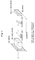
- the first example of construction of the electrical voltage measuring apparatus is shown in Fig. 1.
- a pair of mirrors for resonance 55 and 57 are disposed, between which are a set of a laser medium 51 and an E-O member 53.
- a linearly polarized light is emitted from the laser medium 51. If the light beam emitted from the laser medium 51 is not linearly polarized, it can be linearly polarized by a polarizing element (not shown in the drawing) such as a polarizer or a Brewster Window put after the laser medium 51. The linearly polarized light comes back after entering the E-O member 53 and being reflected by the mirror 55.
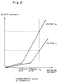
- Output characteristics of the apparatus for the measurement of electrical voltages of Fig. 1 are shown in Fig. 2.
- the output characteristics are those when the voltages at the measured object (not shown in the drawing) are V 1 and V 2 .
- threshold values of excitation intensity and slope efficiencies are different respectively as voltages on the measured object are different.
- the output light varies outstandingly corresponding to a change in the electrical field established in the E-O member 53 or a change in the electrical signal given to the measured object. Accordingly, the voltage at the measured object can be determined with a high S/N (signal-to- noise) ratio by measuring the intensity I of the output light.
- a partially penetrating mirror 59 or a mirror with partial transmittance is disposed between a laser medium 51 and an E-O member 53.
- the laser medium 51 is disposed in a main resonator between the mirror 57 and mirror 59
- the E-O member 53 is disposed in a sub-resonator between the mirror 55 and mirror 57.
- the linearly polarized light from the laser medium 51 is amplified in the main resonator.
- the linearly polarized light partially penetrating the mirror 59 and entering the sub-resonator comes back after reflected by the mirror 55 and converted to elliptically polarized light depending on the electrical field established in the E-O member 53. That is, the resonant status varies in the sub-resonator depending on the voltage at the measured object.
- the output light from the main resonator also reflects the voltage at the local area of the measured object which the E-O member 53 is in the proximity of, affected by the sub-resonator.
- the output characteristics must be the same as those shown in Fig. 2.
- Fig. 4 shows a first embodiment of a voltage measuring apparatus.
- a refractive index of the E-O member 60 varies in response to the electrical field from the measured device, such as, a semiconductor device.
- a light beam emitted by a light source unit 70 which is controlled by a driving apparatus 61 enters the E-O member 60, through a collimating lens 62, a wave plate 63 and a focusing lens 64 in this order.
- Fig. 5 shows an enlarged view of the light source 70.
- a driving signal from a driving apparatus 61 is put on a stripe of a semiconductor laser 71.
- AR (anti-reflection) coating is applied on the bottom face of the semiconductor laser 71.
- the top face is of a cleavaged face and is partially penetrated by a light. It is possible to adjust the penetration ratio or transmittance by forming a mirror at the top face.
- a high reflection mirror is formed on the bottom face of the E-O member 60 shown in Fig. 4.
- the high reflection mirror has a higher reflectance than the top face mirror.
- the high reflection mirror is often formed of a high reflection coating.
- a laser resonator is formed between the top face of the semiconductor laser 71 and the bottom face of the E-O member 60.
- the intensity of the output light emitted from the top face of the semiconductor laser 71 is detected by a photo-detector 72 built in the same package and the result is displayed on an instrument.
- the output of the photo-detector 72 reflects the voltage at the local area of the measured object which the E-O member 60 is in the proximity of.
- a linearly polarized light is emitted from the bottom face of the semiconductor laser 71. If the light beam emitted from the semiconductor laser 71 is not linearly polarized, it can be linearly polarized by a polarizing element (not shown in the drawing) such as a polarizer or a Brewster Window placed between the semiconductor laser 71 and the E-O member 60. The linearly polarized light is converted to an adequate elliptically polarized light by the wave plate 63 and enters the E-O member 60.
- a polarizing element not shown in the drawing
- the linearly polarized light is converted to an adequate elliptically polarized light by the wave plate 63 and enters the E-O member 60.
- a change in a refractive index is caused in the E-O member 60 depending on the intensity of the electrical field established in the E-O member 60, and the status of polarization of the light which is reflected by the high reflectance mirror at the bottom face of the E-O member 60 and emitted from E-O member 60 is changed.
- the high reflectance mirror at the bottom face is formed at the bottom face of the E-O member 60 and has high reflectance characteristics.
- the light passes the wave plate 63 and its polarization status is changed again.
- the light enters an active layer of the semiconductor laser 71 where the light is linearly polarized and causes induced emission or stimulated emission in the active layer at the same time.
- the resonance status of the laser resonator is changed. That is, the intensity of the output light detected by the photo-detector 72 after emitted from the top face of the semiconductor laser 71 reflects the voltage existing at a local area of the measured object which the bottom tip of the E-O member 60 is in the proximity of. Accordingly, the voltage at the measured object can be determined with high sensitivity by measuring the output of the photo-detector 72.
- Fig. 12 The operation principles of the apparatus in Fig. 4 is described in more detail hereunder referring to Fig. 12.
- the curve indicating a relationship between a bias voltage V given to the measured device vs. an intensity I of the output light in Fig. 12 corresponds to that in Fig. 11.
- the curve indicates a characteristic (V-I) in case where the wave plate 63 is not put in position.
- Optical phase in Fig. 12 means a phase difference caused when a laser beam passes a wave plate 63, and is indicated as a phase difference while the laser beam passes the wave plate 63 twice.
- Wave plate in Fig. 12 indicates a relationship between a phase difference and a kind of the wave plates 63.
- phase difference is ⁇ /2 in case of a ⁇ /8 wave plate, and ⁇ in case of a ⁇ /4 wave plate, and further the given voltages V correspond to V ⁇ /2, and V ⁇ respectively.
- an appropriate wave plate 63 should preferably be chosen.
- a ⁇ /8 wave plate 12 is put in the light path to set an optical bias voltage V B and a given voltage V 1 for V ⁇ /2.
- an output intensity detected by the photo detector 72 is attempted to be high through setting an optical bias voltage V B and a given voltage V 3 for a range from V ⁇ /2 to V ⁇ , where the output intensity varies sharply.
- a predetermined voltage V B is determined in a voltage range where a change of the output intensity varies sharply in V-I characteristics.
- the most appropriate range of the voltage V B is from V ⁇ /2 to V ⁇ .
- a wave plate 63 corresponding to the voltage is from ⁇ /8 wave plate to a ⁇ /4 wave plate.
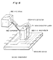
- Fig. 6 shows a second embodiment of an apparatus for measuring voltages. Different from the first embodiment, this embodiment does not need a collimating lens, a wave plate and a focusing lens, and an E-O member 160 is directly attached to the bottom face of the semiconductor laser 171 to be an integrated unit. This integration enables to miniaturize the apparatus to the extent unexpected before.
- the electrical field from the measured device causes a refractive index of the E-O member 160 to vary.
- the light to be detected enters the E-O member 160 directly from the semiconductor laser 171. Since a resonator is formed between the top face of the semiconductor laser 171 and the bottom face of the E-O member 160, the output light detected by the photo-detector 172 fixed at the top of the semiconductor laser 171 is corresponding to the voltage given to the area which the E-O member 160 is in the proximity of.
- the semiconductor laser 171 to which the E-O member 160 is fixed is connected to XYZ stage 190 with a supporter 180.
- the XYZ stage 190 With the XYZ stage 190, it is not necessary to scan the measured object and besides voltage distribution can be determined 2-dimensionally precisely on a minute measured device such as IC.
- the XYZ stage 190 has a stage which can accommodate a measured object and be controlled to move 3-dimensionally.
- a linearly polarized light is emitted from the bottom face of the semiconductor laser 171. This linearly polarized light enters the E-O member 160.
- the E-O member 160 When some voltage is given to the measured object, a change in a refractive index is caused in the E-O member 160 depending on the intensity of the electrical field, and a status of polarization of the light which is reflected by the mirror at the bottom face of the E-O member 160 and emitted from E-O member 160 is changed. Accordingly, the amplitude of the light entering the active layer of the semiconductor laser 171 corresponds to the change in the refractive index of the E-O member 160. After all, the resonance status of the laser resonator can be changed corresponding to the voltage from the measured object.
- the intensity of the output light detected by the photo-detector 172 after being emitted from the top face of the semiconductor laser 171 reflects the voltage existing at a local area of the measured object which the E-O member 160 is in the proximity of. Accordingly, the 2-dimensional distribution of the voltage can be determined with high sensitivity by measuring the output of the photo-detector 172.
- Fig. 7 shows a third embodiment of an apparatus for measuring voltages. This is an embodiment modified from the apparatus of the second embodiment. The same numeral as in the second embodiment is assigned to the corresponding part, and no description is repeated concerning it.
- the device is one in which the semiconductor laser 271 is of GaAs type material. Since a material such as GaAs has electro-optic effect itself, it is not necessary to provide with an E-O member additionally as in Fig. 6. That is, the semiconductor laser 271 itself can have a function of an E-O member without a separate E-O member 160.
- the stripe electrode for inputting electrical current to the semiconductor laser 271 may be partially removed at the measured object side end to give this part high resistance, and consequently the modulation of resonance condition by the electrical field from the measured object or the modulation of the output light to be detected can be of high efficiency.
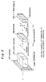
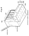
- Fig. 8 shows a fourth embodiment of an apparatus for measuring voltages. This is an embodiment further modified from the apparatus of the second embodiment.
- an LD laser diode
- a surface emitting laser 302 which has a number of luminescence areas within the output face is used, and the formation as indicated in Fig. 3 is adopted.
- a partially penetrating mirror 304 is formed, and in addition an array type photo detector 310 is disposed on the mirror.
- a polished and thin E-O member 308 is attached.
- a high reflection mirror 306 is formed under the member.
- the partially penetrating mirror 304 and the high reflection mirror 306 form a resonator structure.
- Each emitting element of the surface emitting laser 302 luminesces simultaneously responding to the electrical current from the source cable 312 for LD.
- the output from each detecting element of the array type photo-detector leads to a measuring instrument through the output cable 314.
- a CCD charge coupled device
- Fig. 9 shows a fifth embodiment of a voltage measuring apparatus.
- a fiber laser is used, to which an activated substance such as Er (erbium) is added.
- Light output from an exciting light source 473 enters the fiber 471 through DCM (dichroic mirror) 474. Since a resonator structure is formed by the entrance mirror of the fiber 471 and the mirror at the bottom face of the E-O member 460, induced emission of the activated substance in the fiber 471 can cause laser resonance. This kind of resonance status in the laser fiber reflects the refractive index of the E-O member 460.
- the output light to be detected by the photo-detector 472 after being emitted from the mirror 475 and passing through the DCM 474 corresponds to the refractive index of the E-O 460, that is, corresponds to the voltage on the measured object. Accordingly, the voltage distribution on the measured object can be precisely determined by measuring the output of the photo-detector 472 with scanning action of the supported 480.
- the laser medium can be a gas as used for He-Ne laser, Ar laser or the like, or a solid such as Nd:YAG, Ti:sapphire, Cr:LiSAF or the like.
- a change in the electrical field adjacent to the electro-optic member can be sensitively detected from outside, as a change in resonance conditions of laser resonance due to the change in the refractive index caused in the electro-optic member, since the electro-optic member for detecting the electrical field and the laser medium are disposed in the resonator structure.
- the intensity of the laser light emitted from the resonator structure is very sensitive to even a minute change in the refractive index of the electro-optic member, the minute change in the refractive index of the electro-optic member or voltage change at a local area of the measured object or the like can be sensitively detected from the outside without any contact, observing the laser light from outside.
Landscapes
- Physics & Mathematics (AREA)
- General Physics & Mathematics (AREA)
- Measuring Instrument Details And Bridges, And Automatic Balancing Devices (AREA)
- Measurement Of Current Or Voltage (AREA)
- Tests Of Electronic Circuits (AREA)
Claims (9)
- Sonde électro-optique destinée à mesurer des tensions, comprenant :des premier (57, 304) et second (55, 306) moyens réfléchissants ; etun élément (53, 60, 160, 308, 460) électro-optique disposé entre lesdits premier (57, 304) et second (55, 306) moyens réfléchissants pour répondre à un champ électrique externe, l'élément (53, 60, 160, 308, 460) électro-optique ayant des caractéristiques optiques qui varient en fonction du champ électrique ;
caractérisé en ce que lesdits premier (57, 304) et second (55, 306) moyens réfléchissants définissent ensemble un résonateur destiné à fournir en sortie un faisceau lumineux qui varie en fonction d'une variation des caractéristiques optiques de l'élément (53, 60, 160, 308, 460) électro-optique, et par un milieu (51, 71 171, 302, 471) laser disposé dans ledit résonateur pour amplifier ledit faisceau lumineux. - Sonde électro-optique selon la revendication 1, dans laquelle ledit premier moyen (57, 304) réfléchissant a une transmittance vis-à-vis dudit faisceau lumineux, et ledit second moyen (55, 306) réfléchissant a une réflectance plus élevée vis-à-vis dudit faisceau lumineux que ledit premier moyen (57, 304) réfléchissant.
- Sonde électro-optique selon la revendication 1 ou 2, dans laquelle ledit premier moyen (57, 304) réfléchissant est disposé sur une face d'extrémité dudit milieu (51, 71, 171, 302, 471) laser, et ledit second moyen (55, 306) réfléchissant comprend un revêtement fortement réfléchissant qui est disposé sur une face d'extrémité dudit élément (53, 60, 160, 308, 460) électro-optique, afin que ledit milieu (51, 71, 171, 302, 471) laser et ledit élément (53, 60, 160, 308, 460) électro-optique soient disposés entre lesdits premier (57, 304) et second (55, 306) moyens réfléchissants.
- Sonde électro-optique selon l'une quelconque des revendications précédentes, comprenant en outre :un photodétecteur (72, 172, 310, 472) qui détecte une lumière émise par ledit résonateur à travers ledit premier moyen (57, 304) réfléchissant.
- Sonde électro-optique selon l'une quelconque des revendications précédentes, comprenant en outre :une lame d'onde (63) disposée le long du chemin optique dudit faisceau lumineux entre ledit élément (53, 60, 160, 308, 460) électro-optique et ledit milieu (51, 71, 171, 302, 471) laser.
- Sonde électro-optique selon la revendication 5, dans laquelle ladite lame d'onde (63) fournit une tension de polarisation optique qui est dans la gamme de Vπ/2 à Vπ.
- Sonde électro-optique selon l'une quelconque des revendications précédentes, dans laquelle ledit milieu (51, 71, 171, 302, 471) laser comprend une fibre (471) active à effet laser qui couple ledit élément (53, 60, 160, 308, 460) électro-optique à une source (473) de lumière.
- Sonde électro-optique destinée à mesurer des tensions, comprenant :des premier et second moyens réfléchissants ;
caractérisée en ce que lesdits premier et second moyens réfléchissants définissent ensemble un résonateur destiné à délivrer un faisceau lumineux, et par un milieu (271) laser disposé dans ledit résonateur pour amplifier ledit faisceau lumineux et pour répondre à un champ électrique externe, le milieu laser comprenant un matériau électro-optique ayant des caractéristiques optiques qui varient en fonction du champ électrique afin de provoquer une variation du faisceau lumineux délivré par ledit résonateur. - Procédé de mesure d'une tension utilisant la sonde électro-optique selon l'une quelconque des revendications précédentes, comprenant la mise en place de la sonde électro-optique au voisinage d'un objet où une tension doit être mesurée, et la détection d'une variation de la sortie du résonateur.
Applications Claiming Priority (3)
| Application Number | Priority Date | Filing Date | Title |
|---|---|---|---|
| JP23182292A JP3167189B2 (ja) | 1992-08-31 | 1992-08-31 | 電圧測定装置 |
| JP23182292 | 1992-08-31 | ||
| JP231822/92 | 1992-08-31 |
Publications (3)
| Publication Number | Publication Date |
|---|---|
| EP0586202A2 EP0586202A2 (fr) | 1994-03-09 |
| EP0586202A3 EP0586202A3 (fr) | 1995-02-01 |
| EP0586202B1 true EP0586202B1 (fr) | 2000-05-03 |
Family
ID=16929566
Family Applications (1)
| Application Number | Title | Priority Date | Filing Date |
|---|---|---|---|
| EP93306815A Expired - Lifetime EP0586202B1 (fr) | 1992-08-31 | 1993-08-27 | Sonde électro-optique |
Country Status (4)
| Country | Link |
|---|---|
| US (1) | US5444365A (fr) |
| EP (1) | EP0586202B1 (fr) |
| JP (1) | JP3167189B2 (fr) |
| DE (1) | DE69328525T2 (fr) |
Cited By (1)
| Publication number | Priority date | Publication date | Assignee | Title |
|---|---|---|---|---|
| DE102020002735A1 (de) | 2020-05-07 | 2021-11-11 | Protemics GmbH | Photoleitende Messspitze für die ortsaufgelöste Nahfeld-Messung transmittierter und reflektierter Terahertz-Strahlung an Oberflächen |
Families Citing this family (6)
| Publication number | Priority date | Publication date | Assignee | Title |
|---|---|---|---|---|
| WO1995002192A1 (fr) * | 1993-07-07 | 1995-01-19 | Tokin Corporation | Capteur de champs electriques |
| JP3317801B2 (ja) * | 1994-01-12 | 2002-08-26 | 浜松ホトニクス株式会社 | 2次元電圧検出装置 |
| US5734263A (en) * | 1996-02-06 | 1998-03-31 | Eaton Corporaton | Electro-optic voltage transducer with extended range and temperature compensation |
| US7194817B2 (en) | 1999-09-13 | 2007-03-27 | Swagelok Company | Intrinsic gauging for tube fittings |
| JP5376619B2 (ja) | 2008-02-06 | 2013-12-25 | 日本電気株式会社 | 電磁界計測装置 |
| ES2977091A1 (es) * | 2022-12-29 | 2024-08-19 | Airbus Operations Slu | Dispositivo medidor de tensión eléctrica mediante un sistema microelectromecánico con grafeno |
Family Cites Families (9)
| Publication number | Priority date | Publication date | Assignee | Title |
|---|---|---|---|---|
| US4446425A (en) * | 1982-02-12 | 1984-05-01 | The University Of Rochester | Measurement of electrical signals with picosecond resolution |
| DE3311809A1 (de) * | 1983-03-31 | 1984-10-11 | Fraunhofer-Gesellschaft zur Förderung der angewandten Forschung e.V., 8000 München | Interferometrisches, eichbares fabry-perot-sensorsystem mit doppelbrechendem monomode-lichtwellenleiter |
| CA1251846A (fr) * | 1983-09-26 | 1989-03-28 | Masataka Shirasaki | Source de lumiere laser |
| JPS6254991A (ja) * | 1985-09-04 | 1987-03-10 | Hitachi Ltd | 半導体レ−ザ装置 |
| JP2598458B2 (ja) * | 1988-05-31 | 1997-04-09 | 浜松ホトニクス株式会社 | 電気信号観測装置 |
| US4910454A (en) * | 1989-05-23 | 1990-03-20 | The University Of Rochester | System for electrical signal sampling with ultrashort optical pulses |
| GB8923555D0 (en) * | 1989-10-19 | 1989-12-06 | Secr Defence | Bragg cell analyser |
| US5029273A (en) * | 1990-02-02 | 1991-07-02 | The University Of British Columbia | Integrated optics Pockels cell voltage sensor |
| US5041779A (en) | 1990-08-17 | 1991-08-20 | The United States Of America As Represented By The Secretary Of The Army | Nonintrusive electro-optic field sensor |
-
1992
- 1992-08-31 JP JP23182292A patent/JP3167189B2/ja not_active Expired - Fee Related
-
1993
- 1993-08-27 DE DE69328525T patent/DE69328525T2/de not_active Expired - Fee Related
- 1993-08-27 EP EP93306815A patent/EP0586202B1/fr not_active Expired - Lifetime
- 1993-08-30 US US08/113,239 patent/US5444365A/en not_active Expired - Fee Related
Cited By (1)
| Publication number | Priority date | Publication date | Assignee | Title |
|---|---|---|---|---|
| DE102020002735A1 (de) | 2020-05-07 | 2021-11-11 | Protemics GmbH | Photoleitende Messspitze für die ortsaufgelöste Nahfeld-Messung transmittierter und reflektierter Terahertz-Strahlung an Oberflächen |
Also Published As
| Publication number | Publication date |
|---|---|
| JPH0682490A (ja) | 1994-03-22 |
| DE69328525T2 (de) | 2000-09-21 |
| US5444365A (en) | 1995-08-22 |
| JP3167189B2 (ja) | 2001-05-21 |
| EP0586202A3 (fr) | 1995-02-01 |
| EP0586202A2 (fr) | 1994-03-09 |
| DE69328525D1 (de) | 2000-06-08 |
Similar Documents
| Publication | Publication Date | Title |
|---|---|---|
| US5179565A (en) | Low noise pulsed light source utilizing laser diode and voltage detector device utilizing same low noise pulsed light source | |
| US6819812B2 (en) | System and method for measuring physical, chemical and biological stimuli using vertical cavity surface emitting lasers with integrated tuner | |
| US7719666B2 (en) | Distributed optical fiber sensor | |
| De Brabander et al. | Integrated optical ring resonator with micromechanical diaphragms for pressure sensing | |
| US4758087A (en) | Fiber optic transducer | |
| US7049843B2 (en) | Signal acquisition probing system using a micro-cavity laser capable of sensing DC voltages | |
| EP0411641B1 (fr) | Appareil de mesure électro-optique utilisant une diode laser pulsée à faible bruit | |
| EP0586202B1 (fr) | Sonde électro-optique | |
| US7206259B2 (en) | Ultrasound sensor and ultrasound measurement device | |
| US4982151A (en) | Voltage measuring apparatus | |
| EP0347054B1 (fr) | Appareil de corrélation d'intensité lumineuse | |
| JP2941911B2 (ja) | 反射型光走査トンネル顕微鏡 | |
| EP0344986B1 (fr) | Dispositif pour observer des signaux électriques | |
| US4980632A (en) | Electrical signal observing device | |
| US7187187B2 (en) | Signal acquisition probing system using a micro-cavity laser | |
| JP2675419B2 (ja) | 高感度電圧検出装置 | |
| JP2923770B2 (ja) | 光ファイバー構成要素での反射損失を測定する方法及び装置 | |
| JPH06289064A (ja) | ファブリ−ペロ−共振器型電界センサ− | |
| JP2709170B2 (ja) | 電圧測定装置 | |
| JPH07120504A (ja) | 電圧測定装置 | |
| JP3018418B2 (ja) | 光学損失測定装置 | |
| JP3137427B2 (ja) | 光学式微小変位測定装置 | |
| JPH05267408A (ja) | 電界検出装置 | |
| JPH0989940A (ja) | 電界検出装置 | |
| De Brabander et al. | 5, zyxwvutsrqponmlkjihgf |
Legal Events
| Date | Code | Title | Description |
|---|---|---|---|
| PUAI | Public reference made under article 153(3) epc to a published international application that has entered the european phase |
Free format text: ORIGINAL CODE: 0009012 |
|
| AK | Designated contracting states |
Kind code of ref document: A2 Designated state(s): DE FR GB |
|
| PUAL | Search report despatched |
Free format text: ORIGINAL CODE: 0009013 |
|
| AK | Designated contracting states |
Kind code of ref document: A3 Designated state(s): DE FR GB |
|
| 17P | Request for examination filed |
Effective date: 19950502 |
|
| 17Q | First examination report despatched |
Effective date: 19970606 |
|
| GRAG | Despatch of communication of intention to grant |
Free format text: ORIGINAL CODE: EPIDOS AGRA |
|
| RIC1 | Information provided on ipc code assigned before grant |
Free format text: 6G 01R 15/24 A, 6G 01R 31/308 B |
|
| RTI1 | Title (correction) |
Free format text: ELECTRO-OPTIC PROBE |
|
| GRAG | Despatch of communication of intention to grant |
Free format text: ORIGINAL CODE: EPIDOS AGRA |
|
| GRAH | Despatch of communication of intention to grant a patent |
Free format text: ORIGINAL CODE: EPIDOS IGRA |
|
| GRAH | Despatch of communication of intention to grant a patent |
Free format text: ORIGINAL CODE: EPIDOS IGRA |
|
| GRAA | (expected) grant |
Free format text: ORIGINAL CODE: 0009210 |
|
| AK | Designated contracting states |
Kind code of ref document: B1 Designated state(s): DE FR GB |
|
| REF | Corresponds to: |
Ref document number: 69328525 Country of ref document: DE Date of ref document: 20000608 |
|
| ET | Fr: translation filed | ||
| PLBE | No opposition filed within time limit |
Free format text: ORIGINAL CODE: 0009261 |
|
| STAA | Information on the status of an ep patent application or granted ep patent |
Free format text: STATUS: NO OPPOSITION FILED WITHIN TIME LIMIT |
|
| 26N | No opposition filed | ||
| REG | Reference to a national code |
Ref country code: GB Ref legal event code: IF02 |
|
| PGFP | Annual fee paid to national office [announced via postgrant information from national office to epo] |
Ref country code: FR Payment date: 20020808 Year of fee payment: 10 |
|
| PGFP | Annual fee paid to national office [announced via postgrant information from national office to epo] |
Ref country code: GB Payment date: 20020821 Year of fee payment: 10 |
|
| PGFP | Annual fee paid to national office [announced via postgrant information from national office to epo] |
Ref country code: DE Payment date: 20020904 Year of fee payment: 10 |
|
| PG25 | Lapsed in a contracting state [announced via postgrant information from national office to epo] |
Ref country code: GB Free format text: LAPSE BECAUSE OF NON-PAYMENT OF DUE FEES Effective date: 20030827 |
|
| PG25 | Lapsed in a contracting state [announced via postgrant information from national office to epo] |
Ref country code: DE Free format text: LAPSE BECAUSE OF NON-PAYMENT OF DUE FEES Effective date: 20040302 |
|
| GBPC | Gb: european patent ceased through non-payment of renewal fee | ||
| PG25 | Lapsed in a contracting state [announced via postgrant information from national office to epo] |
Ref country code: FR Free format text: LAPSE BECAUSE OF NON-PAYMENT OF DUE FEES Effective date: 20040430 |
|
| REG | Reference to a national code |
Ref country code: FR Ref legal event code: ST |