EP0587208A1 - Méthode confocale et dispositif confocal pour la mise au point dans la lithographie par projection - Google Patents
Méthode confocale et dispositif confocal pour la mise au point dans la lithographie par projection Download PDFInfo
- Publication number
- EP0587208A1 EP0587208A1 EP93202293A EP93202293A EP0587208A1 EP 0587208 A1 EP0587208 A1 EP 0587208A1 EP 93202293 A EP93202293 A EP 93202293A EP 93202293 A EP93202293 A EP 93202293A EP 0587208 A1 EP0587208 A1 EP 0587208A1
- Authority
- EP
- European Patent Office
- Prior art keywords
- radiation
- aperture
- image
- imaging
- subresolution
- Prior art date
- Legal status (The legal status is an assumption and is not a legal conclusion. Google has not performed a legal analysis and makes no representation as to the accuracy of the status listed.)
- Withdrawn
Links
Images



Classifications
-
- G—PHYSICS
- G03—PHOTOGRAPHY; CINEMATOGRAPHY; ANALOGOUS TECHNIQUES USING WAVES OTHER THAN OPTICAL WAVES; ELECTROGRAPHY; HOLOGRAPHY
- G03F—PHOTOMECHANICAL PRODUCTION OF TEXTURED OR PATTERNED SURFACES, e.g. FOR PRINTING, FOR PROCESSING OF SEMICONDUCTOR DEVICES; MATERIALS THEREFOR; ORIGINALS THEREFOR; APPARATUS SPECIALLY ADAPTED THEREFOR
- G03F9/00—Registration or positioning of originals, masks, frames, photographic sheets or textured or patterned surfaces, e.g. automatically
- G03F9/70—Registration or positioning of originals, masks, frames, photographic sheets or textured or patterned surfaces, e.g. automatically for microlithography
- G03F9/7003—Alignment type or strategy, e.g. leveling, global alignment
- G03F9/7023—Aligning or positioning in direction perpendicular to substrate surface
- G03F9/7026—Focusing
-
- G—PHYSICS
- G02—OPTICS
- G02B—OPTICAL ELEMENTS, SYSTEMS OR APPARATUS
- G02B21/00—Microscopes
- G02B21/0004—Microscopes specially adapted for specific applications
- G02B21/002—Scanning microscopes
- G02B21/0024—Confocal scanning microscopes (CSOMs) or confocal "macroscopes"; Accessories which are not restricted to use with CSOMs, e.g. sample holders
- G02B21/0032—Optical details of illumination, e.g. light-sources, pinholes, beam splitters, slits, fibers
-
- G—PHYSICS
- G02—OPTICS
- G02B—OPTICAL ELEMENTS, SYSTEMS OR APPARATUS
- G02B21/00—Microscopes
- G02B21/0004—Microscopes specially adapted for specific applications
- G02B21/002—Scanning microscopes
- G02B21/0024—Confocal scanning microscopes (CSOMs) or confocal "macroscopes"; Accessories which are not restricted to use with CSOMs, e.g. sample holders
- G02B21/0052—Optical details of the image generation
- G02B21/0072—Optical details of the image generation details concerning resolution or correction, including general design of CSOM objectives
Definitions
- This invention generally relates to projection lithography especially as applied to semiconductor integrated circuit fabrication, and, more particularly, to a method and apparatus for focusing the image of a pattern or mask projected onto a photosensitive layer such as a photoresist layer on a semiconductor wafer during the integrated circuit fabrication process.
- the wafer has multiple locations at which fabrication of integrated circuits occurs.
- Present day technology and the unevenness of the photoresist layer on the wafer only allow exposure of one or two chip sites at a time, although many more integrated circuit locations exist on the wafer. Consequently, the wafer used in the process is normally moved to expose the photoresist layer at each location.
- Focusing of the projected image of the mask entails making the top surface of the photoresist layer located on the wafer surface at a particular chip site on the wafer coincident with the image plane of the projection lithography system.
- the oblique system can provide a precise focus of the image of the mask. However, given the extremely close proximity of the imaging lens and the photoresist layer required by the lithographic process, this method can prove difficult at times to implement and in some situations impossible to use.
- Another method of focusing uses air gauges. With this system, air or another gas is blown onto the wafer and measured variations in back pressure caused by differences in distance between the photoresist layer and the imaging lens provide feedback for focusing. However, in addition to requiring calibration, this system can introduce dust particles or other debris that can create errors or defects.
- the third procedure for focusing uses capacitive gauges.
- the capacitive gauge senses changes in capacitance caused by changes in distance between the photoresist surface and lens. Once calibrated, the system can determine the appropriate focus distance between the lens and the photoresist layer located on top of the wafer. However, with this system, differences in capacitance due to differences in the structure of the chip sites or changes from one process step to the next make calibration difficult.
- All of the currently used focusing systems may require recalibration while operating if substantial changes in ambient air pressure occur during the fabrication process. Changes in air pressure cause changes in the refractive index of air which tend to defocus the imaging system, requiring adjustment of the distance between the lens and photoresist layer until the image plane and the photoresist layer are again coincident.
- the confocal imaging principal has been known for some time, but it has not heretofore been suggested that this principal could be applied to overcome the limitations of current focusing techniques in projection lithography.
- the confocal principal has been used primarily on devices related to confocal microscopy and profilometry. These systems generally focus a coherent collimated beam of light such as that produced by a laser or light from a subresolution aperture on a very tiny spot on the specimen to be examined.
- the reflected image from the specimen passes back through the optical system to a detector wherein the specimen reflectance can be utilized to inspect or measure various surface features of the specimen such as surface irregularities, profile, line widths etc.
- the system usually employs a scanning type of imaging procedure that builds up an image based on information obtained sequentially by a series of line or spot scans.
- U.S. Patent 4,863,226 describes one type of confocal scanning microscope.
- U.S. Patent 4,844,617 describes one form of a profilometer.
- the present invention provides a highly sensitive method and apparatus for focusing of an image of an object projected onto a surface which method and apparatus does not require calibration.
- the present invention in one aspect provides a through-the-lens focusing technique which immediately responds to changes which affect the focus of the object to be imaged, e.g. ambient air pressure variations.
- the present invention additionally provides a focusing apparatus and method that can continuously operate while an image of an object projects onto a surface to keep the image of the object in focus on the surface.
- the invention is applicable to various types of projection lithography schemes including step and repeat, scanning type, and pulsed radiation source, and avoids the danger of photoresist overexposure.
- apparatus for focusing an image of an object projected by object imaging means onto an imaging surface.
- the apparatus includes: an electromagnetic radiation barrier having a subresolution aperture therethrough; means for projecting electromagnetic radiation through the aperture towards the imaging surface; confocal imaging means for forming from the projected radiation an image of said aperture in an image plane of the object imaging means, part of the projected radiation reflecting back from a localized region of the imaging surface through the confocal imaging means and the aperture;means for detecting the power of radiation reflected back through the aperture; and means for adjusting the distance between the object imaging means and the imaging surface to maximize the detected power.
- the electromagnetic radiation barrier having the subresolution aperture is located in the same plane as the object.
- the confocal imaging means preferably comprises the object imaging means, and the electromagnetic radiation projected through the aperture preferably is of the same frequency as the radiation which forms the image of the object. The same source of radiant energy can be employed to irradiate the object and the aperture.
- the object comprises a mask and the imaging surface is a photoresist layer on the wafer.
- the localized region of the imaging surface may comprise a sacrificial region of an integrated circuit site or the kerf region between adjacent integrated circuit sites.
- the radiation projected through the aperture can have a power below an exposure threshold of the photoresist layer, or the radiation can be projected through a series of subresolution apertures and the reflected radiation passing through the apertures combined and sensed to avoid the risk of overexposure of the photoresist layer.
- the apparatus may comprise a plurality of subresolution apertures located in the object plane; means for projecting radiation through each of said apertures; confocal imaging means for forming an image of each of said apertures in the image plane of the object imaging means; and means for detecting the power of radiation reflected back through each of the apertures.
- the distance between the object imaging means and the imaging surface can then be adjusted to maximize the detected power of radiation reflected back through all of the apertures.
- the reflected radiation detecting means may include means for distinguishing between reflected radiation originating from the aperture and other radiation, e.g. from the image of the object.
- the radiation projected through the aperture may be pulsed or chopped to produce a periodic variation in intensity and the detecting means may comprise synchronous detection means synchronized with the radiation pulsing or chopping means. If the image of the object is formed from radiant energy emanating from a pulsed source, the radiation projected through the aperture can be pulsed at a rate different from but synchronized with the pulse rate of the radiant energy source.
- the confocal focusing apparatus of the present invention can be employed to calibrate another non-confocal focusing mechanism such as an oblique focus system, a capacitive gauge or an air gauge.
- the present invention also encompasses a method for focusing an image of an object projected by object imaging means onto an imaging surface.
- the method includes the steps of: forming an image of a subresolution aperture in an image plane of the object imaging means; and bringing a localized region of the imaging surface into coincidence with the image of said aperture.
- the image of the aperture is formed by projecting electromagnetic radiation from the aperture through confocal imaging means.
- the power of radiation reflected back from the localized region of the imaging surface through the aperture is detected, and the distance between the object imaging means and the imaging surface is adjusted to maximize the detected power.
- the aperture is located in the object plane; the image of the aperture is formed by the object imaging means; and the same frequency of electromagnetic radiation is employed to form the image of the aperture and the image of the object.
- images of multiple subresolution apertures are formed in the image plane of the object imaging means.
- the invention facilitates focusing of an image of a mask projected by object imaging means onto a photoresist layer during a photolithographic process.
- This method includes the steps of: projecting mask exposure electromagnetic radiation through at least one subresolution aperture located in an electromagnetic radiation barrier located in the plane of the mask; passing the radiation through an electromagnetic radiation imaging device onto a photoresist layer, the imaging device forming an image of the aperture in an image plane of the object imaging means; reflecting a portion of the radiation off the photoresist layer so that it retraces its path back through the imaging device in the aperture; detecting the power of radiation reflected back through the aperture; and adjusting the distance between the photoresist layer and the object imaging means to maximize the detected power of radiation.
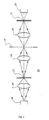
- Fig. 1 depicts schematically a transmissive or unfolded confocal system 10.
- Electromagnetic radiation from a source of electromagnetic radiation 28 passes through lens 19 to focus the radiation on a subresolution aperture of origin 23.
- subresolution aperture 23 is small in size compared to the wavelength of the electromagnetic radiation divided by the numerical aperture of lens 24 on the side facing aperture 23.
- the subresolution aperture may, for example, comprise a "pinhole" or a narrow slit.
- Electromagnetic radiation source 28 projects electromagnetic radiation, generally of a single frequency or narrow range of frequencies, through a beam splitter 32 which passes the electromagnetic radiation on through subresolution aperture of origin 31.
- the transmitted radiation strikes lens 29 which focuses the radiation at a focal point 38 in an image plane 37.
- focal point 38 coincides with a localized region on a surface 39, the system is in focus.
- Surface 39 has reflective qualities which reflect a portion of the radiation back through lens 29.
- the reflected radiation comes to a focus in reflected image plane 33 which is coincident with the subresolution aperture of origin 31 in object plane 35.
- Beam splitter 32 then directs the reflected radiation passing back through aperture 31, to detector 34. While the system remains in focus, detector 34 will detect the maximum possible reflected radiation given the reflective quality of surface 39 and the quality of lens 29.
- Fig. 2B depicts the result of increasing the distance between the surface 39 and the lens 29.
- the image plane 37 created by radiation projected through subresolution aperture 31 and lens 29, no longer coincides with surface 39. Consequently, after the radiation reflects off of surface 39 and passes back through lens 29, the position of reflected image plane 33 has changed. Thus, when the radiation finally reaches object plane 35, it has spread out, no longer being in focus. Thus, only a portion of the reflected radiation passes through aperture 31.
- Detector 34 detects a decrease in the power of light from the maximum detected when the system is in focus.
- Fig. 2C depicts the results of moving surface 39 closer to lens 29 than image plane 37. Radiation reflected back through lens 29 by surface 39 has an actual reflected focus position on reflected image plane 33 which now lies beyond object plane 35. Thus, the returning beam of light is spread out and only a portion of it transmits through subresolution aperture 31 in object plane 35. Consequently, detector 34 detects a decrease in the reflected radiation.
- this reflective confocal approach is advantageously applied to focus a lithographic projection system.
- the subresolution aperture 31 is located in the same plane as the object to be imaged, such as a mask, and radiation of the same frequency as that used to image the object is projected through the subresolution aperture 31.
- the same lens images both the object and the aperture 31 making the confocal system a "through the lens system".
- the image plane of the object and that of the subresolution aperture are the same, namely image plane 37. Consequently, the system does not require calibration since the object exposure radiation in conjunction with the confocal apparatus determines the precise point of focus or location of coincidence of the image plane 37 and surface 39.
- Alternative embodiments could be constructed with separate lenses to image the object and subresolution aperture.
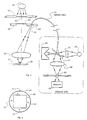
- Fig. 3 depicts the invention incorporated into apparatus used for wafer lithography.
- the confocal system depicted in Fig. 3 has a "through the lens" configuration with all the inherent advantages of such a structure. Since the same lens 29 and electromagnetic radiation of the same frequency are used to image both the aperture 31 and the mask 49 which lie in the same plane 35, no matter what distance exists between the lens 29 of the lithographic apparatus and object plane 35, images of the aperture 31 and mask 49 will always lie in a common image plane 37.
- a diaphragm or lens stop 42 provides a shutter type mechanism, well known in the art, to control passage of electromagnetic radiation from source 28 to mask 49.
- Auxiliary optics may be located along the optical path between source 28 and mask 49, as is common in the art.
- Source 28 provides radiation to image the mask and source 93 provides radiation to image the aperture 31.
- the radiation produced by source 93 strikes beam splitter 32 which reflects approximately half of the radiation up to fiber optic cable 36. Fiber optic cable 36 then directs the radiation through aperture 31.
- Light trap 94 absorbs any radiation from source 93 not reflected up to the cable 36 by beam splitter 32.
- Platen 44 which contains subresolution aperture 31, supports the mask 49 and lies in the same plane as the mask.
- the electromagnetic radiation passing through subresolution aperture 31 strikes lens 29 and comes to a focus at image plane 37.
- the image of the mask 49 and the image of the aperture 31 always lie in common at image plane 37.
- Fiber optic cable 36 then directs the radiation back to beam splitter 32. Approximately half of the radiation passes through beam splitter 32 to lens 92 which focuses the radiation through aperture 95 onto detector 34. Aperture 95 serves to reduce impingement of stray light on detector 34. Use of the above scheme allows for placement of the detector 34 at a remote site.
- detector 34 receives the maximum power of reflected light from surface 39.
- movement of surface 39 to a position at which maximum power is detected assures a precise focusing of image plane 37 on surface 39 without the need for calibration; the nature of the system assuring a precise focus.
- the preferred embodiment depicted uses a lens 29 to create the image plane 37 for both the mask and aperture.
- the electromagnetic radiation used to image the mask may consist of light, infrared or ultraviolet radiation or even soft x-rays.
- the system operates more efficiently when surface 39 moves in relation to the lens to achieve proper focus.
- the mask and lens remain in a fixed relationship while surface 39, at the top of the wafer supported photoresist layer, moves in relationship to the lens 29, i.e. towards or away from the lens to achieve proper focusing.
- the imaging apparatus i.e. mask, lens etc., could move in relation to the wafer to create a focused image of the mask on the photoresist layer.
- Appropriate devices and instruments well known in the art can provide the mechanism by which the readings obtained by the detector 34 control the relative movement and positioning of the wafer and imaging apparatus to achieve focus i.e. coincidence of the image plane 37 and the localized region of the photoresist layer 39.
- the preferred system uses at least three subresolution apertures located in the plane of the mask.
- the apertures can be located on the platen or on the mask itself.
- Fig. 4 is a plan view of a portion of the platen 44 and mask 49 with four subresolution apertures 31 located on the platen 44.
- the radiation reflected back through the subresolution apertures is combined by a detector which senses the total intensity of the radiation and adjusts surface 39 by well known techniques to assure complete coincidence of the localized region of surface 39 and image plane 37.
- the use of the three or more subresolution apertures functions on the well known geometric principal that three or more points define a plane.
- the system of the present invention will not be adversely affected by defocusing effects of changes in ambient air pressure.
- the system given its through the lens nature, automatically corrects for changes in the refractive index due to changes in air pressure.
- the reflective confocal system of the present invention has a sensitivity doubling effect.
- Fig. 2a when the image plane 37 and the surface 39 are coincident, the rays projecting from aperture 31 to image plane 37 demonstrate the in-focus path of the electromagnetic radiation.
- Fig. 2b upon movement of surface 39 a distance "d" away from image plane 37, a virtual image 40 of aperture 31 forms at virtual image plane 41.
- the virtual image plane 41 as indicated lies at a position a distance "2d” from the in-focus position of image plane 37.
- reflected image plane 33 is a distance "2d” from the object plane 35.
- Fig. 2c depicts the same effect when surface 39 moves towards the lens 29 to an out of focus position. The doubling of the effects of surface movements in and out of focus adds an enhanced sensitivity to the system making it more effective.
- a photoresist exposure threshold equals approximately 1X10 ⁇ 6 J/CM2
- a very fast rate at an exposure wavelength of 248 nanometers this requires 4X10⁷ photons per square micrometer.
- the reflectivity of the photoresist layer is 4%
- available photons for focus sensing are approximately 1.6X10⁶ per square micrometer. Consequently, if only one percent of the photons reach the detector there are 1.6X10⁴ photons available, a sufficient number, since this gives a photon-limited signal- to-noise ratio better than 100 to 1.
- a photo-multiplier, solid-state photo detector or similar device can be used for detection. The added sensitivity of the system of the present invention as noted above, with current capabilities of detectors allows use of intensities of radiation for focus determination below those necessary to cause exposure of the photoresist layer.
- One solution involves dedication of a very small region of each integrated circuit site on the wafer as a "sacrificial region". Because of the pin point focusing of the confocal imaging process, only one to two square microns of surface area has to be exposed to implement the present invention. Given the fact that the area of most integrated circuit sites on the wafer varies from 106 to 108 square microns, the actual sacrificial area necessary is minuscule and thus use of such a region creates no appreciable loss of available surface area for the devices of the integrated circuit.
- FIG. 5A provides an overall illustration of a wafer 51 and various integrated circuit or chip sites 53 and the kerf 57 located between them.
- Fig. 5b depicts three integrated circuit sites 53 with the kerf 57 separating them.
- Upon completion of fabrication of the integrated circuits at sites 53 separation of the integrated circuits from each other occurs along the kerf.
- exposure of the kerf to radiation during the focusing process has no negative effect on the integrated circuits.
- a kerf region conveniently surrounds each integrated circuit site.
- the combined reflected radiation provides detector 45 with radiation of sufficient power to make appropriate readings for focusing while at the same time the actual exposure of the photoresist layer to the radiation has been spread out over a sufficiently large enough surface area of the photoresist layer to eliminate any possible over exposure effects on the photoresist layer.
- the number of apertures necessary for such a process depends upon the requisite power necessary for the detector and the threshold sensitivity of the photoresist layer to specific intensities of radiation, all easily determinable once the parameters of the system are known.
- Fig. 7 depicts use of the present system to calibrate an oblique focusing system.
- a fixed spatial relationship would be established between the confocal apparatus 46 and the oblique focusing system with its radiation projector 51 and detection unit 52.
- Surface 39 would be moved, e.g. from position 39b, until it coincides with the image plane 37 as detected by the confocal system, at which position (39a) the reading provided by detection unit 52 would represent the in-focus position of the oblique focusing system.
- position 39a the reading provided by detection unit 52 would represent the in-focus position of the oblique focusing system.
- the system of the present invention has a high degree of flexibility which allows its use with a number of different lithographic fabrication processes currently in use.
- One such system referred to as the step and repeat system involves repositioning of the wafer to align the mask and image projecting system with each successive chip site on the wafer where an exposure of the mask occurs after initiation and completion of focus adjustment.
- the focusing system instead of waiting to activate the focusing system of the present invention until after the imaging apparatus is aligned above the integrated circuit site, the focusing system could continuously operate while the wafer moves.
- the focusing system would be continuously operating until the imaging apparatus becomes positioned above an integrated circuit site and thus achieve a quicker focus.
- Such a procedure would result in reductions of time necessary to fabricate the integrated circuits on the wafer and thus increase overall productivity. This procedure would also reduce the exposure time during the focusing process of any one portion of the photoresist layer and thus reduce the possibility of overexposure.
- Some photolithographic tools use a scanning type of exposure process.
- the mask and imaging apparatus move while exposing an image of the mask on each site as opposed to the step and repeat process mentioned above.
- the mask and imaging apparatus may move continuously or intermittently.
- the confocal focusing method of the present invention could be employed with this continuous process.
- FIG. 8A provides a schematic diagram of an apparatus used for a continuous exposure scanning focus system.
- Rotating beam chopper 73 driven by motor 74 chops the projected beam of electromagnetic radiation up into pulses.
- Chopper 73 typically has alternating radiation transmitting and blocking sections. Consequently, detector 34 senses radiation output patterns as depicted on the graph in Fig. 8b.
- Portion "A" of the detected radiation results from some of the radiation scattered during the exposure of the photoresist reflecting through the aperture.
- Portion "B" of the detected radiation results from the pulses projected through aperture 31.
- the detector 34 in conjunction with conventional synchronous detection electronics 75 easily eliminates the effect of scattered radiation from the readings and makes a correct determination as to intensity of each pulse, thus ensuring proper focusing of the lithographic system. It will be readily apparent to those skilled in the art that methods other than beam chopping can provide radiation in pulses.
- eximer lasers are increasingly used in high resolution photolithography. These lasers emit radiation in a series of pulses making the standard techniques of chopping inappropriate for focus detection.
- One way of applying the confocal focusing technique of the present invention to such systems involves projection of the radiation through the aperture 31 at a rate different from that projected onto the mask. Given the different frequency rates , the system can isolate reflected radiation attributable to pulses projected through the aperture and accordingly focus the system
- One such implementation would project radiation through the aperture with every other pulse of radiation projected onto the mask.
- Fig. 8c provides a graphic representation of the reflected radiation pulses sensed by the detector 34 under such a scheme. The detector easily isolates those portions "C" of every pulse attributable to mask projection radiation reflecting back through the aperture. The detector and associated electronics would then isolate the reflected radiation "D" originally projected through the aperture on every other pulse.
- electromagnetic radiation of the same frequency creates the projected image of both the aperture of origin and the object to be imaged.
- Both the object and the aperture lie in the same plane and the same imaging device, such as a lens, images both.
- the system or method could be very easily altered so that electromagnetic radiation of different frequencies could image the object and the aperture.
- the same imaging device would image both the aperture and object; however, the object and aperture would lie in different but adjacent planes to account for the difference in frequency of imaging radiation used to image the aperture and the object.
- the important factor is assuring the coincidence of the image plane of the object and the image plane of the aperture of origin to maintain the through-the-lens nature of the system or method.
- the imaging device or lens is corrected for axial color, such that it can focus electromagnetic radiation of different frequencies to the same place or image plane, under the right circumstances the same lens can focus both the object and aperture to the same image plane even though they both lie in the same plane when imaged.
- An all reflective system can focus any number of different frequencies to the same plane.
- the subresolution aperture(s) can be made to move, e.g. oscillate, with respect to the object plane in a direction generally perpendicular to the object plane, inorder to determine the location of a surface relative to the image plane.
Landscapes
- Physics & Mathematics (AREA)
- General Physics & Mathematics (AREA)
- Chemical & Material Sciences (AREA)
- Analytical Chemistry (AREA)
- Optics & Photonics (AREA)
- Exposure And Positioning Against Photoresist Photosensitive Materials (AREA)
- Exposure Of Semiconductors, Excluding Electron Or Ion Beam Exposure (AREA)
- Automatic Focus Adjustment (AREA)
Applications Claiming Priority (2)
| Application Number | Priority Date | Filing Date | Title |
|---|---|---|---|
| US07/939,208 US5306902A (en) | 1992-09-01 | 1992-09-01 | Confocal method and apparatus for focusing in projection lithography |
| US939208 | 1997-09-29 |
Publications (1)
| Publication Number | Publication Date |
|---|---|
| EP0587208A1 true EP0587208A1 (fr) | 1994-03-16 |
Family
ID=25472742
Family Applications (1)
| Application Number | Title | Priority Date | Filing Date |
|---|---|---|---|
| EP93202293A Withdrawn EP0587208A1 (fr) | 1992-09-01 | 1993-08-04 | Méthode confocale et dispositif confocal pour la mise au point dans la lithographie par projection |
Country Status (3)
| Country | Link |
|---|---|
| US (1) | US5306902A (fr) |
| EP (1) | EP0587208A1 (fr) |
| JP (1) | JPH06112106A (fr) |
Cited By (4)
| Publication number | Priority date | Publication date | Assignee | Title |
|---|---|---|---|---|
| EP0813115A3 (fr) * | 1996-06-13 | 1999-02-10 | Canon Kabushiki Kaisha | Appareil d'exposition par balayage avec système de détection de la position d'une surface |
| EP0867775A3 (fr) * | 1997-03-27 | 2000-08-02 | Ushiodenki Kabushiki Kaisha | Dispositif d'exposition à proximité avec dispositif de règlage de distance |
| WO2001088590A1 (fr) * | 2000-05-18 | 2001-11-22 | Carl Zeiss Jena Gmbh | Dispositif de mise au point automatique confocale |
| WO2009127322A1 (fr) * | 2008-04-14 | 2009-10-22 | Asml Netherlands B.V. | Capteur de focalisation, appareil d’inspection, appareil lithographique et système de commande |
Families Citing this family (45)
| Publication number | Priority date | Publication date | Assignee | Title |
|---|---|---|---|---|
| US5923430A (en) * | 1993-06-17 | 1999-07-13 | Ultrapointe Corporation | Method for characterizing defects on semiconductor wafers |
| US5483055A (en) * | 1994-01-18 | 1996-01-09 | Thompson; Timothy V. | Method and apparatus for performing an automatic focus operation for a microscope |
| US5521374A (en) * | 1994-09-07 | 1996-05-28 | Lumonics Corporation | Focused laser beam measurement system and method of beam location |
| IL111229A (en) * | 1994-10-10 | 1998-06-15 | Nova Measuring Instr Ltd | Autofocusing microscope |
| US6175754B1 (en) | 1995-06-07 | 2001-01-16 | Keravision, Inc. | Method and apparatus for measuring corneal incisions |
| US5785651A (en) * | 1995-06-07 | 1998-07-28 | Keravision, Inc. | Distance measuring confocal microscope |
| US5713364A (en) * | 1995-08-01 | 1998-02-03 | Medispectra, Inc. | Spectral volume microprobe analysis of materials |
| US6104945A (en) * | 1995-08-01 | 2000-08-15 | Medispectra, Inc. | Spectral volume microprobe arrays |
| US5813987A (en) * | 1995-08-01 | 1998-09-29 | Medispectra, Inc. | Spectral volume microprobe for analysis of materials |
| US6148114A (en) | 1996-11-27 | 2000-11-14 | Ultrapointe Corporation | Ring dilation and erosion techniques for digital image processing |
| US6826422B1 (en) | 1997-01-13 | 2004-11-30 | Medispectra, Inc. | Spectral volume microprobe arrays |
| US6847490B1 (en) * | 1997-01-13 | 2005-01-25 | Medispectra, Inc. | Optical probe accessory device for use in vivo diagnostic procedures |
| US5973316A (en) * | 1997-07-08 | 1999-10-26 | Nec Research Institute, Inc. | Sub-wavelength aperture arrays with enhanced light transmission |
| US6040936A (en) * | 1998-10-08 | 2000-03-21 | Nec Research Institute, Inc. | Optical transmission control apparatus utilizing metal films perforated with subwavelength-diameter holes |
| US6236033B1 (en) | 1998-12-09 | 2001-05-22 | Nec Research Institute, Inc. | Enhanced optical transmission apparatus utilizing metal films having apertures and periodic surface topography |
| JP2002533142A (ja) | 1998-12-23 | 2002-10-08 | メディスペクトラ, インコーポレイテッド | サンプルの光学的試験のためのシステムおよび方法 |
| WO2000036973A1 (fr) * | 1998-12-23 | 2000-06-29 | Medispectra, Inc. | Systemes et techniques optiques destines a l'examen du col |
| US6285020B1 (en) | 1999-11-05 | 2001-09-04 | Nec Research Institute, Inc. | Enhanced optical transmission apparatus with improved inter-surface coupling |
| US7187810B2 (en) * | 1999-12-15 | 2007-03-06 | Medispectra, Inc. | Methods and systems for correcting image misalignment |
| US7260248B2 (en) * | 1999-12-15 | 2007-08-21 | Medispectra, Inc. | Image processing using measures of similarity |
| US20020007122A1 (en) * | 1999-12-15 | 2002-01-17 | Howard Kaufman | Methods of diagnosing disease |
| JP2001311880A (ja) * | 2000-04-28 | 2001-11-09 | Olympus Optical Co Ltd | 小型共焦点光学系 |
| US6441298B1 (en) | 2000-08-15 | 2002-08-27 | Nec Research Institute, Inc | Surface-plasmon enhanced photovoltaic device |
| US6839661B2 (en) | 2000-12-15 | 2005-01-04 | Medispectra, Inc. | System for normalizing spectra |
| US6649901B2 (en) | 2002-03-14 | 2003-11-18 | Nec Laboratories America, Inc. | Enhanced optical transmission apparatus with improved aperture geometry |
| US20040208385A1 (en) * | 2003-04-18 | 2004-10-21 | Medispectra, Inc. | Methods and apparatus for visually enhancing images |
| US7282723B2 (en) * | 2002-07-09 | 2007-10-16 | Medispectra, Inc. | Methods and apparatus for processing spectral data for use in tissue characterization |
| US20040209237A1 (en) * | 2003-04-18 | 2004-10-21 | Medispectra, Inc. | Methods and apparatus for characterization of tissue samples |
| US6933154B2 (en) * | 2002-07-09 | 2005-08-23 | Medispectra, Inc. | Optimal windows for obtaining optical data for characterization of tissue samples |
| US7469160B2 (en) * | 2003-04-18 | 2008-12-23 | Banks Perry S | Methods and apparatus for evaluating image focus |
| US6818903B2 (en) | 2002-07-09 | 2004-11-16 | Medispectra, Inc. | Method and apparatus for identifying spectral artifacts |
| US7309867B2 (en) | 2003-04-18 | 2007-12-18 | Medispectra, Inc. | Methods and apparatus for characterization of tissue samples |
| US7136518B2 (en) * | 2003-04-18 | 2006-11-14 | Medispectra, Inc. | Methods and apparatus for displaying diagnostic data |
| US20040208390A1 (en) * | 2003-04-18 | 2004-10-21 | Medispectra, Inc. | Methods and apparatus for processing image data for use in tissue characterization |
| US7459696B2 (en) | 2003-04-18 | 2008-12-02 | Schomacker Kevin T | Methods and apparatus for calibrating spectral data |
| US7103401B2 (en) | 2002-07-10 | 2006-09-05 | Medispectra, Inc. | Colonic polyp discrimination by tissue fluorescence and fiberoptic probe |
| US6768918B2 (en) * | 2002-07-10 | 2004-07-27 | Medispectra, Inc. | Fluorescent fiberoptic probe for tissue health discrimination and method of use thereof |
| DE10242374A1 (de) * | 2002-09-12 | 2004-04-01 | Siemens Ag | Konfokaler Abstandssensor |
| JP4671695B2 (ja) * | 2002-12-16 | 2011-04-20 | ベルトロニクス,インコーポレイテッド | 弱い光及び蛍光の光の用途において信号対ノイズ比、解像度、又は合焦品質を犠牲にすることなく検査速度を最適化するための方法 |
| KR20070012631A (ko) * | 2003-12-05 | 2007-01-26 | 유니버시티 오브 피츠버그 오브 더 커먼웰쓰 시스템 오브 하이어 에듀케이션 | 금속성 나노-광학 렌즈 및 빔 정형 장치 |
| EP1784678A2 (fr) | 2004-08-19 | 2007-05-16 | University of Pittsburgh | Analyseurs de spectre optiques, de la dimension d'une puce, a resolution accrue |
| US9195124B2 (en) * | 2013-12-20 | 2015-11-24 | Plantronics, Inc. | Automatic projector safety protocols |
| JP2018138990A (ja) | 2016-12-08 | 2018-09-06 | ウルトラテック インク | 再構成ウェハーのリソグラフィ処理のための焦点制御のための走査方法 |
| DE102017223787B3 (de) | 2017-12-22 | 2019-05-09 | Leica Microsystems Cms Gmbh | Verfahren und Vorrichtung zur Bestimmung der Brechzahl eines Probenmediums, nichtflüchtiges computerlesbares Speichermedium und Mikroskop |
| CN114415325B (zh) * | 2022-02-22 | 2023-11-03 | 北京半导体专用设备研究所(中国电子科技集团公司第四十五研究所) | 调焦光学成像系统 |
Citations (3)
| Publication number | Priority date | Publication date | Assignee | Title |
|---|---|---|---|---|
| JPS60180118A (ja) * | 1984-02-27 | 1985-09-13 | Nippon Telegr & Teleph Corp <Ntt> | 回折格子による位置合せ装置 |
| US4689491A (en) * | 1985-04-19 | 1987-08-25 | Datasonics Corp. | Semiconductor wafer scanning system |
| US4844617A (en) * | 1988-01-20 | 1989-07-04 | Tencor Instruments | Confocal measuring microscope with automatic focusing |
Family Cites Families (22)
| Publication number | Priority date | Publication date | Assignee | Title |
|---|---|---|---|---|
| FR2222666B1 (fr) * | 1973-03-19 | 1976-11-05 | Thomson Brandt | |
| JPS5330878A (en) * | 1976-09-03 | 1978-03-23 | Fujitsu Ltd | Focus adjusting device in projection type exposure apparatus |
| AU552364B2 (en) * | 1980-09-02 | 1986-05-29 | Amada Company Limited | Laser cutting |
| JPS57158826A (en) * | 1981-03-27 | 1982-09-30 | Nippon Kogaku Kk <Nikon> | Automatic focusing device for stereoscopical microscope |
| JPS5863906A (ja) * | 1981-10-14 | 1983-04-16 | Olympus Optical Co Ltd | 顕微鏡用合焦位置検出装置 |
| US4556787A (en) * | 1982-03-23 | 1985-12-03 | Olympus Optical Co., Ltd. | Photosensor for optical observing or photographing devices |
| US4634880A (en) * | 1982-04-19 | 1987-01-06 | Siscan Systems, Inc. | Confocal optical imaging system with improved signal-to-noise ratio |
| DE3377814D1 (en) * | 1982-06-05 | 1988-09-29 | Olympus Optical Co | An optical system focus-state detector |
| US4567362A (en) * | 1982-06-25 | 1986-01-28 | Gretag Aktiengesellschaft | Process and apparatus for the focusing of a beam of light on an object |
| DE3339970A1 (de) * | 1983-11-04 | 1985-05-15 | Karl Süss KG, Präzisionsgeräte für Wissenschaft und Industrie GmbH & Co, 8046 Garching | Einrichtung zum automatischen fokussieren von optischen geraeten |
| JPS6236624A (ja) * | 1985-03-27 | 1987-02-17 | Olympus Optical Co Ltd | 走査型光学顕微鏡 |
| JPH0695172B2 (ja) * | 1985-05-28 | 1994-11-24 | オリンパス光学工業株式会社 | 走査型光学顕微鏡 |
| JPS62123415A (ja) * | 1985-11-25 | 1987-06-04 | Canon Inc | 自動焦点検出装置 |
| DE3617421A1 (de) * | 1986-04-30 | 1987-11-05 | Leitz Ernst Gmbh | Optisches bauelement und vorrichtung zu dessen verwendung |
| NL8603108A (nl) * | 1986-12-08 | 1988-07-01 | Philips Nv | Mikroskoop. |
| NL8700612A (nl) * | 1987-03-13 | 1988-10-03 | Tno | Confocale laserscanning microscoop. |
| GB8724575D0 (en) * | 1987-10-20 | 1987-11-25 | Renishaw Plc | Focus detection system |
| FR2626383B1 (fr) * | 1988-01-27 | 1991-10-25 | Commissariat Energie Atomique | Procede de microscopie optique confocale a balayage et en profondeur de champ etendue et dispositifs pour la mise en oeuvre du procede |
| CA1325537C (fr) * | 1988-08-01 | 1993-12-28 | Timothy Peter Dabbs | Microscope a focalisateurs a foyers coincidents |
| DE3828381C2 (de) * | 1988-08-20 | 1997-09-11 | Zeiss Carl Fa | Verfahren und Einrichtung zur automatischen Fokussierung eines optischen Systems |
| US4945220A (en) * | 1988-11-16 | 1990-07-31 | Prometrix Corporation | Autofocusing system for microscope having contrast detection means |
| JPH0323619A (ja) * | 1989-06-21 | 1991-01-31 | Toshiba Corp | 焦点合せ方法およびその装置 |
-
1992
- 1992-09-01 US US07/939,208 patent/US5306902A/en not_active Expired - Fee Related
-
1993
- 1993-06-28 JP JP5157503A patent/JPH06112106A/ja active Pending
- 1993-08-04 EP EP93202293A patent/EP0587208A1/fr not_active Withdrawn
Patent Citations (3)
| Publication number | Priority date | Publication date | Assignee | Title |
|---|---|---|---|---|
| JPS60180118A (ja) * | 1984-02-27 | 1985-09-13 | Nippon Telegr & Teleph Corp <Ntt> | 回折格子による位置合せ装置 |
| US4689491A (en) * | 1985-04-19 | 1987-08-25 | Datasonics Corp. | Semiconductor wafer scanning system |
| US4844617A (en) * | 1988-01-20 | 1989-07-04 | Tencor Instruments | Confocal measuring microscope with automatic focusing |
Non-Patent Citations (2)
| Title |
|---|
| "USE OF A MODULATED LASER BEAM IN AN OPTICAL FOCUS SENSOR AND CONTROL SYSTEM USED IN SEMICONDUCTOR MASK MANUFACTURING", IBM TECHNICAL DISCLOSURE BULLETIN., vol. 30, no. 5, October 1987 (1987-10-01), NEW YORK US, pages 391 - 392 * |
| PATENT ABSTRACTS OF JAPAN vol. 10, no. 20 (E - 376) 25 January 1986 (1986-01-25) * |
Cited By (4)
| Publication number | Priority date | Publication date | Assignee | Title |
|---|---|---|---|---|
| EP0813115A3 (fr) * | 1996-06-13 | 1999-02-10 | Canon Kabushiki Kaisha | Appareil d'exposition par balayage avec système de détection de la position d'une surface |
| EP0867775A3 (fr) * | 1997-03-27 | 2000-08-02 | Ushiodenki Kabushiki Kaisha | Dispositif d'exposition à proximité avec dispositif de règlage de distance |
| WO2001088590A1 (fr) * | 2000-05-18 | 2001-11-22 | Carl Zeiss Jena Gmbh | Dispositif de mise au point automatique confocale |
| WO2009127322A1 (fr) * | 2008-04-14 | 2009-10-22 | Asml Netherlands B.V. | Capteur de focalisation, appareil d’inspection, appareil lithographique et système de commande |
Also Published As
| Publication number | Publication date |
|---|---|
| US5306902A (en) | 1994-04-26 |
| JPH06112106A (ja) | 1994-04-22 |
Similar Documents
| Publication | Publication Date | Title |
|---|---|---|
| US5306902A (en) | Confocal method and apparatus for focusing in projection lithography | |
| TW391035B (en) | Proximity exposure device provided with gap setting mechanism | |
| KR101198347B1 (ko) | 리소그래피 장치 및 디바이스 제조 방법용 레벨 센서 구성부 | |
| US6376329B1 (en) | Semiconductor wafer alignment using backside illumination | |
| JP4163258B2 (ja) | 光学式高さ測定器、このような高さ測定器を有する表面検査デバイス、及びこの検査デバイスを有するリソグラフィックデバイス | |
| KR100623260B1 (ko) | 리소그래피장치 및 디바이스 제조방법 | |
| US8416423B2 (en) | Interferometric apparatus for detecting 3D position of a diffracting object | |
| US6885429B2 (en) | System and method for automated focus measuring of a lithography tool | |
| CN102124411A (zh) | 用于微光刻投射曝光的设备以及用于检查基底表面的设备 | |
| KR100650946B1 (ko) | 방사선 시스템, 리소그래피 장치, 디바이스 제조방법, 및그에 의해 제조된 디바이스 | |
| JPH07270119A (ja) | 集積回路リソグラフィー用の蛍光使用の直接レチクル対ウエハ・アライメントの方法及び装置 | |
| KR100287504B1 (ko) | 면위치검출장치를 구비한 주사노광장치 | |
| KR20010091971A (ko) | 얼라인먼트 장치, 얼라인먼트 방법, 노광 장치 및 노광 방법 | |
| KR20040034480A (ko) | 표유방사선을 결정하는 방법 및 리소그래피 투영장치 | |
| JP2009147332A (ja) | リソグラフィ投影装置で使用する透過像検出デバイス及びこのようなリソグラフィ装置のパターニングデバイス及び/又は投影システムの3次歪みを割り出す方法 | |
| JP2535889B2 (ja) | 投影光学装置 | |
| KR100592822B1 (ko) | 리소그래피장치, 디바이스제조방법 | |
| JPH05118957A (ja) | 投影光学系の検査方法 | |
| US20050112481A1 (en) | Exposure method and apparatus | |
| JP2004165218A (ja) | 露光装置 | |
| JPH0677096B2 (ja) | 投影装置の焦点合せ装置 | |
| JP3211246B2 (ja) | 投影露光装置及び素子製造方法 | |
| JP2010135475A (ja) | 露光装置およびデバイス製造方法 | |
| JPH0640539B2 (ja) | パタ−ン検出方法と該方法を用いた投影光学装置 | |
| JPS62241330A (ja) | 露光装置における位置合わせ方法 |
Legal Events
| Date | Code | Title | Description |
|---|---|---|---|
| PUAI | Public reference made under article 153(3) epc to a published international application that has entered the european phase |
Free format text: ORIGINAL CODE: 0009012 |
|
| AK | Designated contracting states |
Kind code of ref document: A1 Designated state(s): DE FR GB |
|
| 17P | Request for examination filed |
Effective date: 19940718 |
|
| 18D | Application deemed to be withdrawn |
Effective date: 19970301 |