EP0587443B1 - Bild Prozessor und Verfahren - Google Patents
Bild Prozessor und Verfahren Download PDFInfo
- Publication number
- EP0587443B1 EP0587443B1 EP19930307166 EP93307166A EP0587443B1 EP 0587443 B1 EP0587443 B1 EP 0587443B1 EP 19930307166 EP19930307166 EP 19930307166 EP 93307166 A EP93307166 A EP 93307166A EP 0587443 B1 EP0587443 B1 EP 0587443B1
- Authority
- EP
- European Patent Office
- Prior art keywords
- pixels
- row
- memory
- image
- memory arrays
- Prior art date
- Legal status (The legal status is an assumption and is not a legal conclusion. Google has not performed a legal analysis and makes no representation as to the accuracy of the status listed.)
- Expired - Lifetime
Links
- 238000000034 method Methods 0.000 title claims description 14
- 238000003491 array Methods 0.000 claims description 70
- 230000004044 response Effects 0.000 claims description 12
- 239000011159 matrix material Substances 0.000 claims description 7
- 238000012935 Averaging Methods 0.000 claims 2
- 238000010586 diagram Methods 0.000 description 8
- 102100031699 Choline transporter-like protein 1 Human genes 0.000 description 5
- 102100035954 Choline transporter-like protein 2 Human genes 0.000 description 5
- 102100039496 Choline transporter-like protein 4 Human genes 0.000 description 5
- 101000940912 Homo sapiens Choline transporter-like protein 1 Proteins 0.000 description 5
- 101000948115 Homo sapiens Choline transporter-like protein 2 Proteins 0.000 description 5
- 101000889282 Homo sapiens Choline transporter-like protein 4 Proteins 0.000 description 5
- 101100191136 Arabidopsis thaliana PCMP-A2 gene Proteins 0.000 description 1
- 102100039505 Choline transporter-like protein 5 Human genes 0.000 description 1
- 101000889267 Homo sapiens Choline transporter-like protein 5 Proteins 0.000 description 1
- 101100048260 Saccharomyces cerevisiae (strain ATCC 204508 / S288c) UBX2 gene Proteins 0.000 description 1
- 230000000295 complement effect Effects 0.000 description 1
- 230000006835 compression Effects 0.000 description 1
- 238000007906 compression Methods 0.000 description 1
- 238000007796 conventional method Methods 0.000 description 1
- 238000005516 engineering process Methods 0.000 description 1
- 230000006870 function Effects 0.000 description 1
- 238000003672 processing method Methods 0.000 description 1
Images








Classifications
-
- G—PHYSICS
- G11—INFORMATION STORAGE
- G11C—STATIC STORES
- G11C7/00—Arrangements for writing information into, or reading information out from, a digital store
-
- H—ELECTRICITY
- H04—ELECTRIC COMMUNICATION TECHNIQUE
- H04N—PICTORIAL COMMUNICATION, e.g. TELEVISION
- H04N19/00—Methods or arrangements for coding, decoding, compressing or decompressing digital video signals
- H04N19/42—Methods or arrangements for coding, decoding, compressing or decompressing digital video signals characterised by implementation details or hardware specially adapted for video compression or decompression, e.g. dedicated software implementation
-
- H—ELECTRICITY
- H04—ELECTRIC COMMUNICATION TECHNIQUE
- H04N—PICTORIAL COMMUNICATION, e.g. TELEVISION
- H04N19/00—Methods or arrangements for coding, decoding, compressing or decompressing digital video signals
- H04N19/42—Methods or arrangements for coding, decoding, compressing or decompressing digital video signals characterised by implementation details or hardware specially adapted for video compression or decompression, e.g. dedicated software implementation
- H04N19/423—Methods or arrangements for coding, decoding, compressing or decompressing digital video signals characterised by implementation details or hardware specially adapted for video compression or decompression, e.g. dedicated software implementation characterised by memory arrangements
-
- H—ELECTRICITY
- H04—ELECTRIC COMMUNICATION TECHNIQUE
- H04N—PICTORIAL COMMUNICATION, e.g. TELEVISION
- H04N19/00—Methods or arrangements for coding, decoding, compressing or decompressing digital video signals
- H04N19/42—Methods or arrangements for coding, decoding, compressing or decompressing digital video signals characterised by implementation details or hardware specially adapted for video compression or decompression, e.g. dedicated software implementation
- H04N19/436—Methods or arrangements for coding, decoding, compressing or decompressing digital video signals characterised by implementation details or hardware specially adapted for video compression or decompression, e.g. dedicated software implementation using parallelised computational arrangements
-
- H—ELECTRICITY
- H04—ELECTRIC COMMUNICATION TECHNIQUE
- H04N—PICTORIAL COMMUNICATION, e.g. TELEVISION
- H04N19/00—Methods or arrangements for coding, decoding, compressing or decompressing digital video signals
- H04N19/60—Methods or arrangements for coding, decoding, compressing or decompressing digital video signals using transform coding
- H04N19/61—Methods or arrangements for coding, decoding, compressing or decompressing digital video signals using transform coding in combination with predictive coding
-
- H—ELECTRICITY
- H04—ELECTRIC COMMUNICATION TECHNIQUE
- H04N—PICTORIAL COMMUNICATION, e.g. TELEVISION
- H04N5/00—Details of television systems
- H04N5/14—Picture signal circuitry for video frequency region
-
- H—ELECTRICITY
- H04—ELECTRIC COMMUNICATION TECHNIQUE
- H04N—PICTORIAL COMMUNICATION, e.g. TELEVISION
- H04N5/00—Details of television systems
- H04N5/76—Television signal recording
- H04N5/907—Television signal recording using static stores, e.g. storage tubes or semiconductor memories
Definitions
- This invention relates to the processing of digital images, and especially to methods and devices used for processing a digital image in uniform smaller blocks of pixels.
- FIG. 26 shows the configuration of a conventional image memory used for MPEG (Moving Picture Expert Group) encoding, a standard moving picture compression technology.
- This image memory is made of multiple general-purpose DRAM (Dynamic Random Access Memory) 100 and an MPEG interface circuit 102.
- image processing is performed in units of blocks of 8 pixels x 8 lines, each pixel having 8 bits.
- the image information is written into and read from the image memory in units of 8 x 8 blocks.
- the image information for a picture is input in order as 8 x 8 blocks according to prescribed specifications. Consequently, the blocks may be stored in memory regions in several DRAMs 100, which regions correspond to block sites in the image information address space.
- the read operation it should be possible to designate at any site a desired area AR with a size equal to that of the input block unit regardless of the boundaries of the input block units, and it should be possible to designate the desired blocks area by means of the mid-points of the pixel grid, that is, on the half grid.
- 8 x 8 pixels are to be output.
- the MPEG specifications are determined to meet these requirements.
- a larger working block of 9 x 9 pixels containing the desired area is read from DRAM 100 to interface circuit 102 for MPEG processing.
- an 8 x 8 block of averaged pixels is output. In this half-pel processing, the average of the values of the pixels opposite sides of the half grid is taken, and the obtained average value is processed as the pixel on the half grid.
- a DRAM control circuit 104 carries out such functions as write/read control, address generation, allocation of image information, etc., with respect to each DRAM 100.
- the image information of 9 pixels x 9 lines containing the designated area AR are fetched from DRAM 100 and placed in data register 106.
- Adders 108, 110 and 112 are used for the half-pel processing.
- the image information of 8 x 8 pixels in the case of non-half-pel processing or the image information of 8 x 8 pixels after the half-pel processing are temporarily stored in data register 114.
- a half-pel processing control circuit 116 determines whether or not half-pel processing should be carried out in the case of the read operation, based on the address signal from DRAM control circuit 104 designating the area.
- the operation of data registers 106, 114, and adders 108-112 is controlled on the basis of this determination.
- FIG. 27 shows the configuration of DRAM 100.
- this DRAM 100 includes a memory array 120 with multiple memory cells arranged in matrix form; a row decoder 122 and a column decoder 124 which decode and select the memory address in memory array 120 designated by an incoming address signal AD; and a timing control circuit 126 which provides the prescribed timing signals to the various parts of the DRAM 100 in response to external memory control signals RAS-, CAS-.
- the image information for a compressed moving picture is processed, a large-volume, high-speed image memory is needed.
- one set of the specifications include a memory volume of 4 Mb and a write/read cycle time of 35 nsec.
- the aforementioned conventional image memory is made of 4-Mb memory containing 16 parallel-connected 256K (x4) DRAMs for realizing high speed operation.
- the DRAM must be refreshed, and an 8-bit or 10-bit adder is needed to perform half-pel processing for the image information read from DRAM. Consequently, it is impossible to achieve continuous output of the image information for 9 x 9 pixel blocks in a 35 nsec cycle.
- a purpose of the present invention is to address the aforementioned problems of the conventional methods by providing a method and device for image processing in which the write and read operations of the image information can be performed in block units at high speed, and the image information operation can fully meet the specifications as required by the high-speed operation of MPEG, etc..
- US-A 4 758 881 describes a memory for television pictures, having two pairs of memory banks. Luminance data for pixels within each line are stored alternately in the memory banks of a pair, while lines within a field alternate between pairs of memory banks. The least significant bits of the address are used to identify the banks, so that repeatedly incrementing an address register enables the pixel luminance data for a field to be retrieved serially in the correct order. Only two of the four banks are used for chrominance data.
- GB-A 2 092 785 on which the preambles of claims 1 and 6 are based, describes a memory in which data for individual sample points are distributed across four submemories so that any four adjacent points in a square can be read in parallel, one from each submemory, and combined to form interpolated values.
- the invention provides a pipeline image processor for a digital image in the form of a matrix having a grid of pixels in a predetermined number of rows and columns, midpoints between pixels being referenced to a notional half-grid, comprising: a plurality of memory arrays for holding a set of pixels representing the digital image; and address input terminal for receiving an image address signal indicating a designated read area of pixels; a memory control circuit responsive to the image address signal for simultaneously reading pixels of the digital image from the memory arrays; a pixel selector circuit responsive to the image address signal for selecting pixels from the memory arrays; and processing circuitry connected to receive the selected pixels; characterised in that the plurality of memory arrays store the digital image by blocks, each block having a grid of pixels in a predetermined number of rows and columns, so that any four adjacent blocks forming a rectangle in the digital image are stored in different memory arrays, and the plurality of memory blocks are simultaneously readable a block at a time; in that the pixel selector circuitry comprises row selection circuitry for selecting a first
- the invention also provides a method of pipeline image processing a digital image in the form of a matrix having a grid of pixels in a predetermined number of rows and columns to compute averaged midpoints between pixels on a notional half-grid, comprising the steps of: providing a plurality of memory arrays for holding a set of pixels representing the digital image; storing the digital image in the memory arrays; providing an image address signal indicating a designated read area of pixels; simultaneously reading from the memory arrays pixels of the digital image required for computing the designated read area in response to the image address signal; selecting pixels from the memory arrays in response to the image address signal; and processing the selected pixels; characterised in that the step of storing stores the digital image by blocks, each block having a grid of pixels in a predetermined number of rows and columns, so that any four adjacent blocks forming a rectangle in the digital image are stored in different memory arrays, and the plurality of memory blocks are simultaneously readable a block at a time; in that the step of selecting selects a first row of pixels from a first memory
- Figure 1 is a block diagram illustrating the overall configuration of one application example of image memory for MPEG in accordance with the present invention.
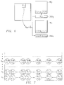
- Figure 2 illustrates an example of the address space MAS of the image of one picture stored in the image memory in the embodiment of Figure 1.
- Figure 3 illustrates the allocation (distribution) of the pixels in the blocks of image information address space MAS.
- Figure 4 illustrates the state when input block B1,1 of row 1 and column 1 is loaded in first data register DREG1 corresponding to first memory array MA1.
- Figure 5 illustrates the state when input block B1,2 of row 1 and column 2 is loaded in second data register DREG2 corresponding to second memory array MA2, while block B1,1 of row 1 and column 1 is transferred from first data register DREG1 to first memory array MA1.
- Figure 6 illustrates the state when input block B1,3 of row 1 and column 3 is loaded in first data register DREGI, while block B1,2 of row 1 and column 2 is transferred from second data register DREG2 to second memory array MA2.
- Figure 7 shows the configuration of the allocation of the image information in first memory array MA1.
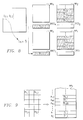
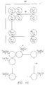
- Figure 8 illustrates the state in which the input row-2 blocks B2,1, B2,2,... are written with a prescribed allocation into third and fourth memory arrays MA3, MA4.
- Figure 9 illustrates the state in which the blocks in the odd-numbered row 4N + 1 in the image information address space are allocated and written in first memory array MA1.
- Figure 10 illustrates the state in which all of the blocks in the image information address space are allocated and written in the first through eighth memory arrays MA1-MA8.
- Figure 11 shows the method of allocation of addresses in this application example.
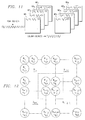
- Figure 12 illustrates the case in which area AR overlapping four blocks Bi,j, Bi,j+1, Bi+1,j, Bi+1,j+1 is designated.
- Figure 13 shows the first pattern of the designated read area.
- Figure 14 shows the second pattern of the designated read area.
- Figure 15 shows the third pattern of the designated read area.
- Figure 16 shows the fourth pattern of the designated read area.
- Figure 17 shows the pattern of the 9 x 9 pixels read from the memory arrays corresponding to the first through fourth read patterns in this application example.
- Figure 18 shows the state of the read operation of the various pixel data of block Bij in row i and column j from first memory array MA1.
- Figure 19 is a circuit diagram illustrating a configuration example of the selector circuit that may be used in column selector XSEL in the application example.
- Figure 20 is a circuit diagram illustrating another configuration example of the selector circuit that may be used in column selector XSEL in the application example.
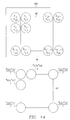
- Figure 21 illustrates the configuration of connection between the output terminal of column selector XSEL and the input terminal of the various operation units of half-pel operation circuit 24.
- Figure 22 is a circuit diagram illustrating the configuration of a circuit of the various operation units of half-pel operation circuit 24.
- Figure 23 is a timing diagram illustrating the operation of first operation unit HPALU1 of half-pel operation circuit 24 in the application example.
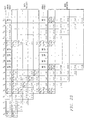
- Figure 24 is a timing diagram illustrating the state of the parallel operation of the first through eighth operation units HPALU1-HPALU8 of half-pel circuit 24 in the application example.
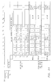
- Figure 25 is a timing diagram illustrating the operation of the operation unit when the read operation of one designated read area is switched to the read operation of another designated read area.
- Figure 26 is a block diagram illustrating the configuration of the conventional image memory for MPEG.
- Figure 27 illustrates a typical configuration of DRAM used for the conventional image memory.
- FIG. 1 shows the overall configuration of the image memory for MPEG in an application example of this invention.
- This information memory is manufactured in the form of 1-chip memory with a volume of 4 Mb.
- image memory unit 10 is made of 8 conventional memory arrays MA1-MA8 connected in parallel.
- each memory array MAi can perform write/read of the individual image information under control of write address generating circuit 12, memory array control logic 14, and read address generating circuit 16.
- the input/output terminals of memory arrays MA1-MA8 are connected to 8 data registers DREG1-DREG8, respectively of an input/output buffer 18.
- Each data register DREGi performs serial-in/parallel-out operation in write mode and parallel-in/parallel out operation in read mode.
- Each data register DREGi has 512 bits, and so can store 8 x 8 pixels of 8 bits each (one block) of the image information at a time.
- the image information, in 8 x 8 pixel blocks, is input to and output from each memory array MAi through the corresponding data register DREGi.
- the output terminals of data registers DREG1-DREG8 can be respectively connected to the input terminals of the 8 row selectors YSEL1-YSEL8 of selector circuit 20. Each of these row selectors YSEL1-YSEL8 can select the pixels belonging to a prescribed row from the block read by one memory array MAi.
- the output terminals of row selectors YSEL1-YSEL8 are connected to the input terminals of a common column selector XSEL. This column selector XSEL is used for selecting the pixels in columns within the designated area AR from the pixels of the rows selected by the row selectors YSEL1-YSEL8.
- the output terminals of the column selector XSEL are connected to the input terminals of half-pel processing operation circuit 24 via data bus 22 of 9 pixels x 2 bits.
- the half-pel processing operation circuit 24 is made of 8 operation units HPALU1-HPALU8. These operation units HPALU1-HPALU8 perform half-pel operate in parallel to procedure respective output pixels 1-8. In this way, half-pel processing is carried out one row at a time.
- the output terminals of operation units HPALU1-HPALU8 are connected to respective input terminals of 8 registers DG1-DG8 of a data register 26. These registers DG1-DG8 have their output terminals connected in common to a data output buffer 28.
- the output terminals of data output buffer 28 are connected to an 8-bit data output bus 30.
- the write operation to image memory unit 10 is carried out under control of write address generating circuit 12 and memory array control logic 14. In the following, the write operation will be explained with reference to Figures 2-10.
- Figure 2 shows an example of address space MAS of the image information of one picture stored in the image memory.
- Figure 3 shows the allocation (distribution) of the pixels in the blocks of image information address space MAS.
- one picture of 720 pixels x 480 lines is divided in matrix form into 90 x 60 (5400) blocks B1,1, B1,2,...B60,90 according to image processing format.
- each block Bi,j contains 8 pixels x 8 lines of pixels (of 8 bits each).
- the one-picture image information having the aforementioned image information address space can be obtained from the receiving/demodulation unit of a TV receiver.
- block B1,1 of the first block row and first block column is loaded as input data D in into first data register DREG1.
- block B1,2 of the first row and second column is loaded as input data D in into second data register DREG2.
- block B1,2 is loaded into second data register DREG2
- block B1,1, which has been loaded into first data register DREGI is transferred to the first row of first memory array MA1.
- This transfer command is generated by memory array control logic 14.
- block B1,3 in first row and third column is loaded as input data D in into first data register DREG1, block B1,2, which has been loaded into second data register DREG2, is transferred to the first row of second memory array MA2.
- blocks B1,1-B1,90 of the first row blocks B1,1, B1,3,...B1,89 of the odd columns are written in order into first memory array MA1 through first data register DREG1, and blocks B1,2, B1,4,...B1,90 of the even columns are written in order into second memory array MA2 through second data register DREG2.
- Figure 7 shows the memory map illustrating the configuration of the image information in first information array MA1.
- Stored in the first row (row A1) of first memory array MA1 are the data for the 64 pixels B1,1, a1,1; B1,1, a1,2;...B1,1, a1,8;...B1,1, a8,8 contained in block B1,1 of the first row and first column in image information address space MAS.
- Stored in the second row (row A2) of first memory array MA1 are the data for the 64 pixels B1,3, a1,1; B1,3, a1,2;...B1,3, a1,8;...B1,3, a8,8 contained in block B1,3 of the first row and third column in image information address space MAS.
- rows 1-45 of first memory array MA1 store the data for the 64 pixels contained in each of the 45 blocks B1,1, B1,3,...B1,89 of the odd-numbered columns in the first row.
- rows 1-45 of second memory array MA2 store the data for the 64 pixels contained in each of the 45 blocks B1,2, B1,4,...B1,90 of the even-numbered columns in the first row, respectively.
- first-row blocks B1,1, B1,2,...B1,90 are written into first and second memory arrays MA1, MA2, respectively.
- second-row blocks B2,1, B2,2,...B2,90 are written into third and fourth memory arrays MA3, MA4, respectively. That is, from among the blocks B2,1-B2,90 of the second row, blocks B2,1, B2,3,...B2,89 of the odd columns are written in order into third memory array MA3 through third data register DREG3, and blocks B2,2, B2,4,...B2,90 of the even columns are written in order into fourth memory array MA4 through fourth data register DREG4.
- third-row blocks B3,1, B3,2,...B3,90 are written into fifth and sixth memory arrays MA5, MA6 through fifth and sixth data registers DREG5 and DREG6, respectively.
- fourth-row blocks B4,1, B4,2,...B4,90 are written into seventh and eighth memory arrays MA7, MA8 through seventh and eight data registers DREG7 and DREG8, respectively.
- blocks B1,1,...B4,90 in rows 1-4 are written into the eight memory arrays MA1-MA8.
- fifth-row blocks B5,1, B5,2,...B5,90 are written into first and second memory registers MA1 and MA2, respectively.
- first memory array MA1 after first-row odd-numbered-column blocks B1,1,...B1,89, fifth-row odd-numbered-column blocks B5,1, B5,3,...B5,89 are stored in order into memory addresses A45, A46,..., respectively.
- second memory array MA2 after first-row even-numbered-column blocks B1,2,...B1,90, fifth-row even-numbered-column blocks B5,2, B5,4,...B5,90 are stored in order.
- the image information of one picture is written in 8 x 8 pixel block units into 8 memory arrays MA1-MA8.
- the blocks in the odd-numbered columns and even-numbered columns in row (4N + 2) are stored in third and fourth memory arrays MA3 and MA4, 1 block/1 row at a time;
- the blocks in the odd-numbered columns and even-numbered columns in row (4N + 3) are stored in fifth and sixth memory arrays MA5 and MA6, 1 block/1 row at a time;
- the blocks in the odd-numbered columns and even-numbered columns in row (4N + 4) are stored in seventh and eighth memory arrays MA7 and MA8, 1 block/1 row at a time.
- Figure 11 shows the allocation of the addresses in this application example.
- the memory address is generated as a 19-bit address signal, which is a special combination, to be explained later, of 10 bits of X-address (X9, X8,...X0) and 9 bits of Y-address (Y8, Y7,...Y0), by a write generating circuit 12.
- Each address value corresponds to a pixel datum (8 bits).
- Write generating circuit 12 has an address counter; it starts the operation corresponding to write reset signal RSTW-, and it generates the write address signal with an increment of unity for each period of clock signal CLCK
- memory address control logic 14 provides the desired command signals to the various memory arrays MAi and various data registers DREGi.
- X-address (X9, X8,...X0) and Y-address (Y8, Y7,...Y0) correspond to the addresses (coordinates) of the image address space MAS in the X direction and Y direction, respectively.
- the lower 3 bits (X2, X1, X0) of the X-address represent the positions of the various columns within a block Bi,j
- the lower 3 bits (Y2, Y1, Y0) of the Y-address represent the positions of the various rows within a block Bi,j. Consequently, the 6-bit addresses formed of these lower 3 bits (Y2, Y1, Y0, X2, X1, X0) represent the allocation positions of the 64 pixels within any block Bij.
- the 6-bit address (Y2, Y1, Y0, X2, X1, X0) is the column address representing the position of any of the 64 pixels, that is, the position of one of the columns, within a block stored as a row of a memory array MAi.
- the fourth bit (X3) in the X-address, counting from the lower bit takes on value "0" for blocks in even-numbered columns and value "1" for blocks in odd-numbered columns in image address space MAS.
- this bit (X3) takes on value "0” for the odd-numbered memory arrays MA1, MA3, MA5 and MA7, and value "1" for the even-numbered memory arrays MA2, MA4, MA6, and MA8.
- These two bits take on the values "0,” “0” for row 4N + 1, the values "0,” “1” for row 4N + 2, the values "1," "0” for row 4N + 3, and the values "1,” "1” for row 4N + 4.
- these two bits take on the values "0,” “0” for the first and second memory arrays MA1, MA2, the values “0,” “1” for third and fourth memory arrays MA3, MA4, the values "1,” “0” for fifth and sixth memory arrays MA5, MA6, and the values "1,” “1” for seventh and eighth memory arrays MA7, MA8.
- the upper 6 bits (X9, X8, X7, X6, X5, X4) of the X-address represent positions among the odd-numbered columns or positions among the even-numbered columns. Namely, each row contains 45 odd-numbered column blocks and 45 even-numbered blocks. These 45 odd-numbered column blocks or 45 even-numbered blocks within a row are continuously written into a corresponding memory array MAi, one block/one line at a time.
- the 10-bit address (Y8, Y7, Y6, Y5, X9, X8, X7, X6, X5, X4) made up of a sum of the upper 6 bits of the X-address (X9, X8, X7, X6, X5, X4) and the upper 4 bits of the Y-address (Y8, Y7, Y6, Y5) is the row address which represents the position of a row of each memory array MAi.
- the read operation in the image memory in this application example will be explained with reference to Figures 12-25.
- the read operation is performed in units of the size of a block.
- agreement with the blocks Bi,j of the matrix form into which the image was divided in the write operation may be present or absent, and an area with the same size 8 x 8 as a block Bi,j, designated at any site in image information address space MAS, can be externally designated.
- the address which represents the upper-left end position of the desired area in image information address space MAS is input as external address A in to the read address generating circuit 16.
- read start signal BRAS- is input into read address generating circuit 16 and memory address control logic 14.
- read address signal needed for reading the image information in the corresponding area with reference to said external address A in is generated in the period of clock CLCK.
- memory address control logic 14 sends the necessary command signals to the various memory arrays MAi and various data registers DREGi.
- Figure 12 shows the case when area AR extends to the four blocks Bi,j, Bi,j+1, Bi+1,j, Bi+1,j+1.
- the size of the assigned read area AR is constant at 8 x 8
- the first pattern has the pixels of area AR in agreement with the grids of the various blocks.
- the pixels Bi,j, a3,6 in block Bi,j of row i and column j are assigned the upper-left position of area AR by external address signal A in .
- the 8 x 8 pixel information in area AR, Bi,j, a3,6; Bij, a3,7;...Bi+1,j+1, d2,5 are read and directly output.
- the pixels of the assigned read area AR are located on the midpoints between the existing X grid points, that is, on the X half-grids, of the various blocks.
- the midpoint between pixels Bi,j, a3,6 and Bi,j, a3,7 in block Bij of row i and column j is assigned as the upper-left position of area AR by means of external address signal A in .
- external address signal A in has a Y address with an integer value and an X address to one decimal place (0.5).
- the adjacent pixels can be read from blocks Bi,j, Bi,j+1, Bi,j, Bi+1,j+1.
- the average value is derived in the half-pel processing, and these average values are output as the 8 x 8 pixel information in area AR.
- This processing for deriving the average value is known as half-pel processing in the X (horizontal) direction.
- the pixels of the assigned read area AR are located at the midpoints of the Y grid points, that is, on the Y half-grids, of the various blocks.
- the midpoint between pixels Bi,j, a3,6 and Bi,j, a4,6 in block Bi,j of row i and column j is assigned the upper-left position of area AR by means of external address signal A in .
- external address signal A in has an X address with an integer value and a Y address to one decimal place (0.5).
- the adjacent pixels can be read from blocks Bi,j, Bi,j+1, Bi+1,j, Bi+1,j+1.
- the average value is derived in half-pel processing, and this average value is output as the 8 x 8 pixel information in area AR.
- the pixels of the assigned read area AR are located at the midpoints of the X and Y grid points, that is, on the XY half-grids, of the various blocks.
- the half-grid of four pixels Bij, a3,6; Bi,j, a3,7; Bi,j, a4,6 and Bi,j, a4,7 in block Bi,j of row i and column j is assigned the upper-left position of area AR by means of external address signal A in .
- external address signal A in has both an X address and a Y address to one decimal place (0.5).
- the average value is derived with the half-pel processing, and this average value is output as the 8 x 8 pixel information in area AR.
- 9 x 9 pixels can be read from the adjacent four blocks Bi,j, Bi,j+1, Bi+1,j, Bi+1,j+1.
- the read image information is then sent to half-pel processing circuit 24.
- These adjacent four blocks Bij, Bi,j+1, Bi+1,j, Bi+1,j+1 are stored in different memory arrays. For example, they may be stored in the first, second, third, and fourth memory arrays MA1, MA2, MA3, and MA4, respectively.
- reading of the 9 x 9 pixel information shown in Figure 17 is carried out under control of read address generating circuit 16 and memory array control logic 14 by means of the aforementioned four memory arrays MA1-MA4, the four data registers DREG1-DREG4 related to them, four row selectors YSEL1- YSEL4, and column selector XSEL.
- Figure 18 illustrates the state of transfer of information for the 64 pixels a1,1, a1,2,...a1,8, a2,1,...a8,8 in block Bi,j from first memory array MA1 to first data register DREGI in a parallel format.
- the 64 pixels of information a1,1, a1,2,...a1,8, a2,1,...a8,8 in block Bi,j transferred to first data register DREG1 are each 8-bit data.
- Each piece of pixel information is transferred in 4 cycles, with 2 bits per cycle, from the lower bit, from first data register DREG1 to first row selector Y SEL1.
- First row-selector YSEL1 receives the lower 3 bits of the Y-address (Y2, Y1, Y0) from read address generating circuit 16, and it selects the pixels located on the row within the block assigned by the three bits of address.
- row-3 pixels a3,1, a3,2,...a3,8 initially designated by these three bits of address are pixels on the third row a3,1, a3,2,...a3,8. Consequently, from the eight output terminals y1, y2,...y8 of first row-selector YSEL1, the 8-bit data of the 8 pixels in row-3 in block Bi,j are transferred to column selector XSEL in 4 cycles, two bits per cycle.
- Column selector XSEL receives the lower 3 bits (X2, X1, X0) of the X-address from read address generating circuit 16, and selects the column in the particular range designated by these 3 bits of address.
- the 3 bits of X-address (X2, X1, X0) designate the column of the pixels in the upper-left corner of the area Bi,j, a3,6, that is, column 6.
- column selector XSEL selects the pixels of the sixth and higher columns a3,6, a3,7, a3,8 for block Bi,j, and the pixels of the sixth and lower columns b3,1, b3,2, b3,3, b3,4, b3,5, b3,6 for block Bi,j+1.
- these selected 9 pixels a3,6, a3,7, a3,8, b3,1, b3,2, b3,3, b3,4, b3,5, b3,6 are input to half-pel processing circuit 24 through data bus 22 from the 9 output terminals x1, x2,...x9, in four cycles, with two bits per cycle, from the lowest bit.
- the various pixels in the second row a4,6, a4,7, a4,8, b4,1, b4,2, b4,3, b4,4, b4,5, b4,6 are read in four cycles, with two bits per cycle;
- the various pixels in the third row a5,6, a5,7, a5,8, b5,1, b5,2, b5,3, b5,4, b5,5, b5,6 are read in four cycles, with two bits per cycle;
- the various pixels in the last row, the ninth row c3,6, c3,7, c3,8, d3,1, d3,2, d3,3, d3,4, d3,5, d3,6 are read in four cycles, with two bits per cycle.
- Figure 19 shows an example of a selector circuit used as column selector XSEL.
- this selector circuit 3 bits of X-address (X2, X1, X0) are input, and all of the output signals SEi, SEi+1,... higher than the value Pi of address (X2, X1, X0) are set on "H” level. That will not be described in detail. It is a dynamic type decoder. SE1-SE8 are maintained at "L” in the standby condition.
- the selected output (one out of Z1-Z8) becomes “H,” and the remaining nonselected outputs become floating “L.”
- output terminal Z6 of decoder 32 becomes “H,” while the output terminals become the floating state "L.”
- MOS transistor TR7A connected to output terminal Z7 of the adjacent upper decoder is turned on, and decoder output terminal Z7 also becomes “H.”
- decoder output terminal Z8 also becomes “H.”
- All of lower decoder output terminals Z1 to Z5 remain as “L.”
- the upper 3 output signals SE6-SE8 become “H”
- the 6 lower output signals SE1-SE5 become “L.”
- Figure 20 shows an example of the configuration of a selector circuit which can be used in column selector XSEL.
- the selector circuit in Figure 20 is made of gate circuits.
- Figure 21 illustrates the configuration of connection between output terminals x1, x2,...x9 of column selector XSEL and the input terminals of operation units HPALU1-HPALU8 of half-pel processing circuit 24.
- the upper bits x1u and x2u of output terminals x1, x2 of column selector XSEL are connected to upper bit input terminals SAU and SBU of first operation unit HPALU1, respectively.
- the lower bits x1L and x2L of output terminals x1, x2 are connected to lower bit input terminals SAL and SBL of first operation unit HPALU1, respectively.
- Upper bit x2u and lower bit x2L of output terminal x2 are also connected to upper bit input terminal SAU on one side and lower bit input terminal SAL on the other side of second operation unit HPALU2, respectively.
- the other upper bit input terminal SBU and lower bit input terminal SEL of second operation unit HPALU2 are connected to upper bit x3u and lower bit x3L of output terminal x3, respectively.
- the other output terminals x4-x9, 2 bits for each of them, are connected to the input terminals of the other operation units HPALU3-HPALU8, respectively.
- Figure 22 shows an example of the configuration of the circuit of various operation units HPALUi.
- first 2-position full adder circuit 44 made of a pair of half-adders 40, 42 and second full adder circuit 50 made of a pair of half-adders 46, 48 are connected to each other in series.
- data register 52 with a size of 2 x 5 bits.
- second adder circuit 50 is connected to data register 54 with a size of 2 x 5 bits.
- the carry output terminal C 0 of first adder circuit 44 is directly connected to one input terminal A of half-adder circuit 56, it is also connected to the other input terminal B of half-adder circuit 56 via a one-bit register 58.
- that read pattern corresponds to the case in which the pixels of the designated area AR are located at the middle point between the X-grids and Y-grids of the various blocks, that is, on the XY half grids.
- half-pel processing is performed to derive the average value of the adjacent 4 pixels in both the X-direction and Y-direction.
- the derived average values are output as 8 x 8 pixel information in area AR.
- the average value pixel of the first column, first row is generated as (a3,6 + a3,7 + a4,6 + a4,7)/4 in first operation unit HPALU1; for example, the average value pixel of the second column, first row is generated as (a3,7 + a3,8 + a4,7 + a4,8)/4 in second operation unit HPALU2; and, for example, the average value pixel of the eighth column, first row is generated as (b3,5 + b3,6 + b4,5 + b4,6)/4 in eighth operation unit HPALU8.
- first operation unit HPALU1 In the following, the operation of first operation unit HPALU1 will be explained with reference to Figures 22 and 23.
- first clock cycle T1 lowest bits a3,6(1), a3,7(1) of pixels a3,6, a3,7 are input through AND gates 60, 62 to two input terminals A, B of half-adder 40 for lower bit of first adder circuit 44, respectively.
- Half-adder 40 adds these bits a3,6(1), a3,7(1), and outputs the sum from output terminal S.
- the carry In the case when a carry is generated, the carry is output from carry output terminal CO.
- the sum is stored in data register 52, and the carry is sent to carry input terminal Ci of half-adder 42 for the upper bit.
- next lowest bits a3,6(2), a3,7(2) of pixels a3,6, a3,7 are input through AND gates 64, 66 to two input terminals A, B of half-adder 42 for upper bit, respectively.
- Half-adder 42 adds these bits a3,6(2), a3,7(2), and any carry bit received, and outputs the sum from output terminal S.
- the carry is output from carry output terminal CO.
- the sum is stored in data register 52, and the carry is stored in register 70.
- the carry is sent from this register 70 to carry input terminal Ci of half-adder 40 via AND gate 68.
- third lowest bits a3,6(3), a3,7(3) of pixels a3,6, a3,7 are input through AND gates 60, 62 to two input terminals A, B of half-adder 40 for lower bit of first adder circuit 44, respectively.
- Half-adder 40 adds these bits a3,6(3), a3,7(3) and any carry from the preceding two lower bits a3,6(1,2), a3,7(1,2), and outputs the sum from output terminal S.
- the carry is output from carry output terminal CO.
- the sum is stored in data register 52 in FIFO format, and the carry is sent to carry input terminal Ci of half-adder 42 for the upper bit.
- fourth lowest bits a3,6(4), a3,7(4) of pixels a3,6, a3,7 are input through AND gates 64, 66 to two input terminals A, B of half-adder 42 for upper bit, respectively.
- Half-adder 42 adds these bits a3,6(4), a3,7(4) and any carry, and outputs the sum from output terminal S.
- the carry is output from carry output terminal CO.
- the sum is stored in data register 52 in the FIFO format, and the carry is stored in register 70.
- the carry is sent from this register 70 to carry input terminal Ci of half-adder 40 via AND gate 68.
- pixels a4,6, a4,7 in columns 1 and 2 in row 2 are input by means of column register XSEL into first operation unit HPALU1 in four cycles, with 2 bits per cycle, from the lowest bit.
- the addition operation is performed for the lowest bits a4,6(1), a4,7(1) of pixels a4,6, a4,7 at half-adder 40.
- the addition operation is performed for the second lowest bits a4,6(2), a4,7(2) of pixels a4,6, a4,7 at half-adder 42.
- the sums of the two lower bits of pixels a4,6, a4,7, namely, (a4,6(1) + a4,7(1)); (a4,6(2) + a4,7(2), output from said half-adders 40, 42 are stored in the FIFO format into data register 52.
- AND gates 72, 74 they are input to one input terminal B of half-adder circuits 46, 48 of second adder circuit 50.
- Half-adder circuit 46 performs the addition operation for the aforementioned two inputs a4,6(1) + a4,7(1); a3,6(1) + a3,7(1), and it sends the sum from output terminal S. When a carry is generated, it is output from carry output terminal CO. The value of the sum is loaded in data register 54 in the FIFO format. Any carry is input into carry input terminal Ci of half-adder 48.
- Half-adder circuit 48 performs the addition operation for the aforementioned two inputs a4,6(2) + a4,7(2); a3,6(2) + a(3,7(2) and any carry, and it sends the sum from output terminal S.
- a carry is generated, it is output from carry output terminal CO.
- the value of the sum is loaded in data register 54 in the FIFO format. Any carry is input into carry input register 78. In the next cycle, the carry is sent from this register 78 to carry input terminal Ci of half-adder 46 via AND gate 76.
- first adder circuit 44 performs the addition operation of the third bits counted from the lowest bit a4,6(3), a4,6(3) and the fourth bits counted from the lowest bit a4,6(4), a4,6(4) of pixels a4,6, a4,7 in the second row, respectively.
- the sum of the third bits counted from the lowest bit a3,6(3), a3,7(3) and the sum of the fourth bits counted from the lowest bit a3,6(4), a3,7(4) of the row-1 pixels a3,6, a3,7 from data register 52 are added, respectively, to the sum of the third bits counted from the lowest bit a4,6(3), a4,7(3) and the sum of the fourth bits counted from the lowest bit a4,6(4), a4,7(4) of the row-2 pixels a4,6, a4,7 obtained in the first adder circuit 44.
- the sum of the third and fourth bits counted from the lowest bit of the four pixels a3,6, a3,7, a4,6, a4,7 obtained from second adder circuit 50 is loaded in the FIFO format to data register 54.
- cycle T7 the sum of the fifth and sixth bits counted from the lowest bit of the four pixels a3,6, a3,7, a4,6, a4,7 is derived.
- cycle T8 a sum of the seventh and eighth bits counted from the lowest bit of the four pixels a3,6, a3,7, a4,6, a4,7 is derived. These sums are loaded successively in data register 54.
- the carry generated by half-adder 42 for the upper bit of first adder circuit 44 is input to input terminal A of half-adder 56, and it is also loaded into register 58.
- pixels a5,6, a5,7 in columns 1 and 2 in row 3 in the 9 x 9 working block corresponding to read area AR are input by means of column selector XSEL into first operation unit HPALU1, in 4 cycles, with 2 bits per cycle.
- First adder circuit 44 then performs the same operation as above, and these pixels a5,6, a5,7 are added from the lowest bit in 4 cycles T13-T16, with 2 bits per cycle.
- second adder circuit 50 the same operation as above is also performed, and the sum of these pixels a5,6, a5,7 and the sum of pixels a4,6, a4,7 stored in data register 52 are added from the lowest bit in 4 cycles T13-T16, with 2 bits per cycle.
- half-adder 56 adds the carry of the sum of pixel a4,6, a4,7 and the carry of the sum of pixels a5,6, a5,7, and the sum (10 bits) of the four pixels a4,6, a4,7, a5,6, a5,7, which surround the half grid on row 2 and column 1 in designated read area AR is stored in data register 54, and the average value pixel (a4,6 + a4,7 + a5,6 + a5,7)/4 is sent from said data register 54 to first register DG1 of data register 26.
- Figure 24 illustrates the state of the parallel operation of the eight operation units HPALU1-HPALU8 in half-pel operation circuit 24.
- Figure 25 shows the state in which, soon after 8 x 8 pixels are output for an assigned read area AR, the processing for the next assigned read area AR is started at the various operation units HPALUi.
- control signals CTL1, CTL2, CTL4 are set selectively on levels of "H” and "L” corresponding to YES/NO of requirement on the half-pel processing.
- the image information of the read area AR designated at an arbitrary site is to the read out at 8 x 8 size
- the image information of the various blocks Bi,j are read together to data registers DREGi from 1-4 independent memory arrays related to the aforementioned area
- the desired pixels are sent first from data registers DREGi in the pipeline format, two bits at a time, to various operation units HPALUi of half-pel operation circuit 24; at various operation units HPALUi, the two input pixels are added, two bits at a time, from the lowest bit; at the same time, the sum is added to the two bits corresponding to the sum of the two pixels of the preceding row.
- eight memory arrays MA1-MA8 are used. However, this number is not a necessity. For example, it is also possible to use four memory arrays MA1-MA4.
- the main point required in this invention is that it has a configuration which allows allocation of multiple, for example, 80 x 60, blocks to multiple memory arrays so that all of the blocks adjacent to an arbitrary block can be stored in corresponding memory arrays different from that of the aforementioned arbitrary block.
- the image memory of this invention may also be used in applications other than MPEG. For example, it is possible to perform the write operation in units of 1 row instead of 8 x 8 blocks, and to perform the read operation from any site in size of 8 x 8 as above.
- the various operation units of the half-pel operation circuit have a configuration corresponding to addition from the lowest bit with 2 bits at a time.
- that circuit may also have a configuration in which the addition operation is carried out from the lowest bit, with 4 bits at a time.
- multiple blocks are allocated to multiple memory arrays so that all of the blocks adjacent to an arbitrary block are stored in the corresponding memory arrays different from the aforementioned arbitrary block; when a read area is designated at any site and with the same size as the block, the image information is read simultaneously from the adjacent blocks at least partially overlapped with the aforementioned read area; then, the half-pel processing is carried out so as to extract the necessary image information corresponding to the designated read area from the read image information; in this way, the desired pixels can be output at a high rate.
- the half-pel processing method of this invention the operation is carried out using a pipeline format; hence, the desired pixels can be output without interruption. Consequently, this invention can also be used for MPEG and other specifications with sufficient margin.
Landscapes
- Engineering & Computer Science (AREA)
- Multimedia (AREA)
- Signal Processing (AREA)
- Computing Systems (AREA)
- Theoretical Computer Science (AREA)
- Compression Or Coding Systems Of Tv Signals (AREA)
- Compression Of Band Width Or Redundancy In Fax (AREA)
- Controls And Circuits For Display Device (AREA)
- Dram (AREA)
- Image Input (AREA)
- Image Processing (AREA)
- Control Of Indicators Other Than Cathode Ray Tubes (AREA)
Claims (9)
- Pipeline-Bildprozessor für ein digitales Bild in Form einer Matrix, die ein Gitter aus Pixeln (ai,i) in einer vorgegebenen Anzahl von Zeilen und Spalten enthält, wobei die Mittelpunkte zwischen Pixeln als imaginäres Halbgitter bezeichnet werden, mit: mehreren Speichermatrizen (MA1-MA8) zum Halten einer das digitale Bild darstellenden Menge von Pixeln; einem Adresseneingangsanschluß (Ain) zum Empfangen eines Bildadressensignals, das einen bezeichneten Adressenbereich (AR) von Pixeln angibt; einer Speichersteuerschaltung (14), die auf das Bildadressensignal anspricht, um gleichzeitig Pixel des digitalen Bildes aus den Speichermatrizen zu lesen; einer Pixelwählschaltung, die auf das Bildadressensignal anspricht, um Pixel aus den Speichermatrizen zu wählen; und einer Verarbeitungsschaltungsanordnung, die so angeschlossen ist, daß sie die ausgewählten Pixel empfängt; dadurch gekennzeichnet, daß die mehreren Speichermatrizen das digitale Bild in Blöcken (B1,1-B60,90) speichern, wovon jeder ein Gitter aus Pixeln in einer vorgegebenen Anzahl von Zeilen und Spalten (A1,1-A8,8) besitzt, so daß irgendwelche vier benachbarten Blöcke, die im digitalen Bild ein Rechteck bilden, in verschiedenen Speichermatrizen (MA) gespeichert werden und die mehreren Speicherblöcke gleichzeitig blockweise gelesen werden können; daß die Pixelwählschaltungsanordnung versehen ist mit einer Zeilenwählschaltungsanordnung (YSEL) zum Wählen einer ersten Zeile von Pixeln aus einer ersten Speichermatrix (MA1) der mehreren Speichermatrizen, zum Wählen einer zweiten Zeile aus Pixeln aus einer zweiten Speichermatrix (MA2) der mehreren Speichermatrizen, zum Wählen einer dritten Zeile von Pixeln aus einer dritten Speichermatrix (MA3) der mehreren Speichermatrizen und zum Wählen einer vierten Zeile von Pixeln aus einer vierten Speichermatrix (MA4) der mehreren Speichermatrizen und mit einer Spaltenwählschaltungsanordnung (XSEL) zum Wählen eines Teils der ersten Zeile von Pixeln und eines Teils der zweiten Zeile von Pixeln, um als Antwort auf das Bildadressensignal eine erste Pixel-Arbeitszeile zu bilden, und zum Wählen eines Teils der dritten Zeile von Pixeln und eines Teils der vierten Zeile von Pixeln, um als Antwort auf das Bildadressensignal eine zweite Pixel-Arbeitszeile zu bilden; und daß die Verarbeitungsschaltungsanordnung (24) gleichzeitig jedes Pixel der ersten Pixel-Arbeitszeile bearbeitet, um eine Zeile berechneter Pixel des bezeichneten Lesebereichs auszugeben.
- Bildprozessor nach Anspruch 1, dadurch gekennzeichnet, daß die Verarbeitungsschaltungsanordnung mehrere Halbbildelement-Operationseinheiten (HPALU1-HPALU8) enthält, wovon jede so betreibbar ist, daß sie gleichzeitig ein berechnetes Pixel im Halbgitter bildet, indem sie den Durchschnitt zweier aus der ersten Pixel-Arbeitszeile gewählter Pixel und zweier aus der zweiten Pixel-Arbeitszeile gewählter Pixel bildet und eine Zeile berechneter Pixel des bezeichneten Lesebereichs (AR) des Halbgitters ausgibt.
- Bildprozessor nach Anspruch 2, dadurch gekennzeichnet, daß die Verarbeitungsschaltungsanordnung eine Halbbildelement-Operationseinheit (HPALU1-HPALU8) für jede Spalte des bezeichneten Lesebereichs (AR) enthält, wovon jede umfaßt: einen horizontalen Addierer (44) zum Mitteln eines horizontal benachbarten Paars von Pixeln aus der ersten Pixel-Arbeitszeile als ein momentanes horizontal gemitteltes Pixel; ein internes Pixelregister (52) zum Speichern des momentanen horizontal gemittelten Pixel; und einen vertikalen Addierer (50) zum Mitteln eines horizontal benachbarten Paars von Pixeln aus der zweiten Pixel-Arbeitszeile mit dem im internen Pixelregister (52) gespeicherten horizontal gemittelten Pixel, um ein berechnetes Pixel des bezeichneten Halbbereichs (AR) des Halbgitters auszugeben.
- Bildprozessor nach irgendeinem der Ansprüche 1 bis 3, dadurch gekennzeichnet, daß jede Speichermatrix (MA) ein entsprechendes Datenregister (DREG) zum Empfangen und Halten eines Blocks von Pixeln aus der Speichermatrix, der einem gesamten Block von Pixeln entspricht, enthält; und die PixelWählschaltungsanordnung für jedes Datenregister (DREG) eine entsprechende Zeilenwähleinrichtung (YSEL) enthält, die auf das Bildadressensignal anspricht, um sequentiell jede Zeile des Blocks auszugeben, der in dem Datenregister gehalten wird und für die Berechnung des bezeichneten Lesebereichs (AR) erforderlich ist.
- Bildprozessor nach irgendeinem der Ansprüche 1 bis 4, dadurch gekennzeichnet, daß die Zeilenwählschaltungsanordnung (XSEL) auf das Bildadressensignal (Mai) anspricht, um aus jeder von der Zeilenwählschaltungsanordnung (YSEL) ausgegebenen Zeile genau jene Pixel auszuwählen, die für die Berechnung des bezeichneten Lesebereichs (AR) als eine Zeile von Arbeitspixeln erforderlich sind.
- Verfahren zur Pipeline-Bildverarbeitung eines digitalen Bildes in Form einer Matrix, die ein Gitter aus Pixeln (ai,i) in einer vorgegebenen Anzahl von Zeilen und Spalten enthält, um gemittelte Mittelpunkte zwischen Pixeln in einem imaginären Halbgitter zu berechnen, mit den folgenden Schritten: Bereitstellen mehrerer Speichermatrizen (MA1-MA8) zum Halten einer das digitale Bild darstellenden Menge von Pixeln; Speichern des digitalen Bildes in den Speichermatrizen; Erzeugen eines Bildadressensignals (Ain), das einen bezeichneten Lesebereich (AR) von Pixeln angibt; gleichzeitiges Lesen von Pixeln des digitalen Bildes, die für die Berechnung des bezeichneten Lesebereichs (AR) erforderlich sind, als Antwort auf das Bildadressensignal (Ain) aus den Speichermatrizen; Wählen von Pixeln aus den Speichermatrizen als Antwort auf das Bildadressensignal; und Verarbeiten der ausgewählten Pixel; dadurch gekennzeichnet, daß der Schritt des Speicherns das digitale Bild in Blöcken (B1,1-B60,90) speichert, wovon jeder ein Gitter aus Pixeln (a1,1-a8,8) in einer vorgegebenen Anzahl von Zeilen und Spalten besitzt, so daß irgendwelche vier benachbarten Blöcke, die im digitalen Bild ein Rechteck bilden, in verschiedenen Speichermatrizen gespeichert sind und die mehreren Speicherblöcke gleichzeitig blockweise gelesen werden können; daß der Schritt des Wählens eine erste Zeile von Pixeln aus einer ersten Speichermatrix (MAl) der mehreren Speichermatrizen, eine zweite Zeile von Pixeln aus einer zweiten Speichermatrix (MA2) der mehreren Speichermatrizen, eine dritte Zeile von Pixeln aus einer dritten Speichermatrix (MA3) der mehreren Speichermatrizen und eine vierte Zeile von Pixeln aus einer vierten Speichermatrix (MA4) der mehreren Speichermatrizen wählt und ferner als Antwort auf das Bildadressensignal einen Abschnitt (a3,6-a3,8) der ersten Zeile von Pixeln und einen Abschnitt (B3,1-B3,6) der zweiten Zeile von Pixeln wählt, um eine erste Pixel-Arbeitszeile zu bilden, und einen Abschnitt (a1,6-a1,8) der dritten Zeile von Pixeln und einen Abschnitt (B4,1-B4,6) der vierten Zeile von Pixeln wählt, um eine zweite Pixel-Arbeitszeile zu bilden; und daß der Schritt des Verarbeitens gleichzeitig jedes Pixel der ersten Pixel-Arbeitszeile verarbeitet, um eine Zeile berechneter Pixel des bezeichneten Lesebereichs auszugeben.
- Verfahren nach Anspruch 6, dadurch gekennzeichnet, daß der Schritt des gleichzeitigen Verarbeitens mehrere berechnete Pixel im Halbgitter bildet, indem er für jedes derartige berechnete Pixel den Mittelwert zweier Pixel, die aus der ersten Pixel-Arbeitszeile gewählt sind, und zweier Pixel, die aus der zweiten Pixel-Arbeitszeile gewählt sind, bildet und eine Zeile berechneter Pixel des bezeichneten Lesebereichs (AR) im Halbgitter ausgibt.
- Verfahren nach Anspruch 7, dadurch gekennzeichnet, daß der Schritt des Verarbeitens das gleichzeitige Ausführen einer Halbbildelement-Operation für jede Spalte des bezeichneten Lesebereichs (AR) enthält, wovon jede umfaßt: Addieren eines horizontal benachbarten Paars von Pixeln aus der ersten Pixel-Arbeitszeile als momentanes horizontal addiertes Pixel; Speichern des momentanen horizontal gemittelten Pixel; Addieren eines horizontal benachbarten Paars von Pixeln aus der zweiten Pixel-Arbeitszeile zu dem gespeicherten horizontal gemittelten Pixel; und Dividieren durch vier, um ein berechnetes Pixel des bezeichneten Halbbereichs (AR) im Halbgitter zu bilden.
- Verfahren nach irgendeinem der Ansprüche 6 bis 8, dadurch gekennzeichnet, daß der Schritt des Wählens als Antwort auf das Bildadressensignal (Mai) das Wählen genau jener Pixel, die für die Berechnung des bezeichneten Lesebereichs (AR) als eine Zeile von Arbeitspixeln erforderlich sind, aus jeder von der Zeilenwählschaltungsanordnung (YSEL) ausgegebenen Zeile umfaßt.
Applications Claiming Priority (3)
| Application Number | Priority Date | Filing Date | Title |
|---|---|---|---|
| JP26958292A JP3278756B2 (ja) | 1992-09-10 | 1992-09-10 | 画像処理方法及び装置 |
| JP26958292 | 1992-09-10 | ||
| JP269582/92 | 1992-09-10 |
Publications (3)
| Publication Number | Publication Date |
|---|---|
| EP0587443A2 EP0587443A2 (de) | 1994-03-16 |
| EP0587443A3 EP0587443A3 (de) | 1995-06-07 |
| EP0587443B1 true EP0587443B1 (de) | 1999-06-30 |
Family
ID=17474374
Family Applications (1)
| Application Number | Title | Priority Date | Filing Date |
|---|---|---|---|
| EP19930307166 Expired - Lifetime EP0587443B1 (de) | 1992-09-10 | 1993-09-10 | Bild Prozessor und Verfahren |
Country Status (4)
| Country | Link |
|---|---|
| US (1) | US5878173A (de) |
| EP (1) | EP0587443B1 (de) |
| JP (1) | JP3278756B2 (de) |
| DE (1) | DE69325487T2 (de) |
Families Citing this family (22)
| Publication number | Priority date | Publication date | Assignee | Title |
|---|---|---|---|---|
| GB9405914D0 (en) * | 1994-03-24 | 1994-05-11 | Discovision Ass | Video decompression |
| US5768629A (en) * | 1993-06-24 | 1998-06-16 | Discovision Associates | Token-based adaptive video processing arrangement |
| US6330644B1 (en) * | 1994-10-27 | 2001-12-11 | Canon Kabushiki Kaisha | Signal processor with a plurality of kinds of processors and a shared memory accessed through a versatile control means |
| EP0714212A3 (de) * | 1994-11-21 | 1999-03-31 | SICAN, GESELLSCHAFT FÜR SILIZIUM-ANWENDUNGEN UND CAD/CAT NIEDERSACHSEN mbH | Bilddekodierer mit konkurrierender Verarbeitung und Verteilung von Verarbeitungseinheiten |
| US5831881A (en) * | 1994-12-02 | 1998-11-03 | Sican Gmbh | Method and circuit for forward/inverse discrete cosine transform (DCT/IDCT) |
| DE4442957C2 (de) * | 1994-12-02 | 2002-06-06 | Sci Worx Gmbh | Verfahren zur Speicherung von digitalen Datenfeldern |
| WO1996033575A1 (en) * | 1995-04-18 | 1996-10-24 | Advanced Micro Devices, Inc. | Video decoder using block oriented data structures |
| DE19549306A1 (de) * | 1995-12-22 | 1997-07-03 | Art & Com Medientechnologie Un | Verfahren und Vorrichtung zur bildlichen Darstellung raumbezogener Daten |
| KR0183927B1 (ko) * | 1996-09-20 | 1999-04-15 | 삼성전자주식회사 | 복호화장치 |
| JPH10143131A (ja) * | 1996-11-06 | 1998-05-29 | Toshiba Corp | 復号画像表示装置とその表示メモリ制御方法 |
| US6289053B1 (en) * | 1997-07-31 | 2001-09-11 | Lsi Logic Corporation | Architecture for decoding MPEG compliant video bitstreams meeting 2-frame and letterboxing requirements |
| US6335950B1 (en) * | 1997-10-14 | 2002-01-01 | Lsi Logic Corporation | Motion estimation engine |
| FR2780184B1 (fr) | 1998-06-23 | 2000-08-11 | St Microelectronics Sa | Procede et dispositif de decodage d'images, permettant un nombre reduit d'ouvertures de pages-memoire dans le traitement de prediction |
| WO2000008844A1 (de) * | 1998-08-06 | 2000-02-17 | Infineon Technologies Ag | Verfahren zum wahlfreien zugriff auf bildblöcke in videobildern |
| US6747656B2 (en) * | 2000-04-07 | 2004-06-08 | Sony Corporation | Image processing apparatus and method of the same, and display apparatus using the image processing apparatus |
| US6796715B2 (en) | 2001-04-14 | 2004-09-28 | E20 Communications, Inc. | Fiber optic modules with pull-action de-latching mechanisms |
| US9292904B2 (en) | 2004-01-16 | 2016-03-22 | Nvidia Corporation | Video image processing with parallel processing |
| US7308159B2 (en) * | 2004-01-16 | 2007-12-11 | Enuclia Semiconductor, Inc. | Image processing system and method with dynamically controlled pixel processing |
| EP1605400A1 (de) * | 2004-06-11 | 2005-12-14 | STMicroelectronics S.r.l. | Verarbeitungspipeline von Pixeldaten eines Farbe Bildes durch einen digitalen Sensor erworben |
| US7869666B2 (en) | 2005-01-13 | 2011-01-11 | Nvidia Corporation | Video processing system and method with dynamic tag architecture |
| US20060245642A1 (en) * | 2005-04-29 | 2006-11-02 | Stmicroelectronics S.R.L. | Software implemented image generating pipeline using a dedicated digital signal processor |
| CN100383849C (zh) * | 2005-12-27 | 2008-04-23 | 上海大学 | 有机电致发光显示屏的列控制电路 |
Family Cites Families (15)
| Publication number | Priority date | Publication date | Assignee | Title |
|---|---|---|---|---|
| US4174514A (en) * | 1976-11-15 | 1979-11-13 | Environmental Research Institute Of Michigan | Parallel partitioned serial neighborhood processors |
| US4460958A (en) * | 1981-01-26 | 1984-07-17 | Rca Corporation | Window-scanned memory |
| US4524455A (en) * | 1981-06-01 | 1985-06-18 | Environmental Research Inst. Of Michigan | Pipeline processor |
| EP0085210A1 (de) * | 1982-01-29 | 1983-08-10 | International Business Machines Corporation | Bildverarbeitungssystem |
| US4633503A (en) * | 1984-03-19 | 1986-12-30 | The United States Of America As Represented By The Secretary Of The Navy | Video zoom processor |
| EP0184547B1 (de) * | 1984-12-07 | 1991-11-21 | Dainippon Screen Mfg. Co., Ltd. | Bilddatenverarbeitungsverfahren und System dafür |
| FR2582132B1 (fr) * | 1985-05-15 | 1987-07-17 | O Donnell Ciaran | Circuit de memoire d'image virtuelle permettant le multifenetrage |
| JPS6247786A (ja) * | 1985-08-27 | 1987-03-02 | Hamamatsu Photonics Kk | 近傍画像処理専用メモリ |
| US4797945A (en) * | 1985-12-13 | 1989-01-10 | Canon Kabushiki Kaisha | Image data coding apparatus |
| US4758881A (en) | 1987-06-02 | 1988-07-19 | Eastman Kodak Company | Still video frame store memory |
| GB2229059B (en) * | 1989-03-07 | 1993-08-04 | Sony Corp | Obtaining access to a two-dimensional portion of a digital picture signal |
| US5402513A (en) * | 1991-10-15 | 1995-03-28 | Pixel Semiconductor, Inc. | Video window generator with scalable video |
| JP2549479B2 (ja) * | 1991-12-06 | 1996-10-30 | 日本電信電話株式会社 | 動き補償フレーム間帯域分割符号化処理方法 |
| US5247355A (en) * | 1992-06-11 | 1993-09-21 | Northwest Starscan Limited Partnership | Gridlocked method and system for video motion compensation |
| US5398079A (en) * | 1993-01-27 | 1995-03-14 | General Instrument Corporation | Half-pixel interpolation for a motion compensated digital video system |
-
1992
- 1992-09-10 JP JP26958292A patent/JP3278756B2/ja not_active Expired - Fee Related
-
1993
- 1993-09-10 EP EP19930307166 patent/EP0587443B1/de not_active Expired - Lifetime
- 1993-09-10 DE DE69325487T patent/DE69325487T2/de not_active Expired - Fee Related
-
1996
- 1996-10-16 US US08/730,993 patent/US5878173A/en not_active Expired - Lifetime
Also Published As
| Publication number | Publication date |
|---|---|
| JPH0695631A (ja) | 1994-04-08 |
| JP3278756B2 (ja) | 2002-04-30 |
| EP0587443A3 (de) | 1995-06-07 |
| DE69325487T2 (de) | 1999-12-30 |
| US5878173A (en) | 1999-03-02 |
| EP0587443A2 (de) | 1994-03-16 |
| DE69325487D1 (de) | 1999-08-05 |
Similar Documents
| Publication | Publication Date | Title |
|---|---|---|
| EP0587443B1 (de) | Bild Prozessor und Verfahren | |
| EP0895216B1 (de) | Bildspeicheranordnung und Bildzugriffverfahren | |
| EP0264726B1 (de) | Speicher zur Bildtransformation | |
| JPH02208690A (ja) | 表示メモリとそれを備えた画像処理装置 | |
| KR0122741B1 (ko) | 병렬 구조를 갖는 기억 장치 | |
| US6593965B1 (en) | CCD data pixel interpolation circuit and digital still camera equipped with it | |
| US5675826A (en) | Image data storage | |
| JP4224876B2 (ja) | 記憶装置、並びに書き込み方法および読み出し方法 | |
| US6424753B1 (en) | Pixel interpolation method and circuit therefor | |
| KR100233765B1 (ko) | 화상 기억 방법 및 그 장치 | |
| US5412740A (en) | Signal processing system having reduced memory space | |
| KR100528560B1 (ko) | 계층적 코딩에 이용하기 위한 저장 장치 및 기록 및 판독 방법 | |
| CA1287398C (en) | Electronic image processing circuit | |
| EP0827082A1 (de) | Halbleiterspeicher mit arithmetikfunktion und verwendung desselben in einem prozessor | |
| US5638310A (en) | Pixel matrix filter | |
| US6108746A (en) | Semiconductor memory having an arithmetic function and a terminal arrangement for coordinating operation with a higher processor | |
| US5151976A (en) | Device for converting a line scanning into a vertical saw tooth scanning through stripes | |
| US6046753A (en) | Electronic image processing system for modifying initial image data | |
| US6486885B2 (en) | Memory device and method | |
| JP4156538B2 (ja) | 行列演算装置 | |
| KR960011738B1 (ko) | 프레임 및 필드 구조에 따른 어드레스 발생장치 | |
| JP2000284771A (ja) | 映像データ処理装置 | |
| JPH0417471B2 (de) | ||
| JPH0213196A (ja) | 半導体画像メモリ | |
| US20050147326A1 (en) | Pixellated image data sub-sampling |
Legal Events
| Date | Code | Title | Description |
|---|---|---|---|
| PUAI | Public reference made under article 153(3) epc to a published international application that has entered the european phase |
Free format text: ORIGINAL CODE: 0009012 |
|
| AK | Designated contracting states |
Kind code of ref document: A2 Designated state(s): DE FR GB IT NL |
|
| PUAL | Search report despatched |
Free format text: ORIGINAL CODE: 0009013 |
|
| AK | Designated contracting states |
Kind code of ref document: A3 Designated state(s): DE FR GB IT NL |
|
| 17P | Request for examination filed |
Effective date: 19951201 |
|
| 17Q | First examination report despatched |
Effective date: 19970702 |
|
| GRAG | Despatch of communication of intention to grant |
Free format text: ORIGINAL CODE: EPIDOS AGRA |
|
| GRAG | Despatch of communication of intention to grant |
Free format text: ORIGINAL CODE: EPIDOS AGRA |
|
| GRAH | Despatch of communication of intention to grant a patent |
Free format text: ORIGINAL CODE: EPIDOS IGRA |
|
| GRAH | Despatch of communication of intention to grant a patent |
Free format text: ORIGINAL CODE: EPIDOS IGRA |
|
| GRAA | (expected) grant |
Free format text: ORIGINAL CODE: 0009210 |
|
| AK | Designated contracting states |
Kind code of ref document: B1 Designated state(s): DE FR GB IT NL |
|
| PG25 | Lapsed in a contracting state [announced via postgrant information from national office to epo] |
Ref country code: IT Free format text: LAPSE BECAUSE OF FAILURE TO SUBMIT A TRANSLATION OF THE DESCRIPTION OR TO PAY THE FEE WITHIN THE PRESCRIBED TIME-LIMIT;WARNING: LAPSES OF ITALIAN PATENTS WITH EFFECTIVE DATE BEFORE 2007 MAY HAVE OCCURRED AT ANY TIME BEFORE 2007. THE CORRECT EFFECTIVE DATE MAY BE DIFFERENT FROM THE ONE RECORDED. Effective date: 19990630 |
|
| REF | Corresponds to: |
Ref document number: 69325487 Country of ref document: DE Date of ref document: 19990805 |
|
| ET | Fr: translation filed | ||
| PLBE | No opposition filed within time limit |
Free format text: ORIGINAL CODE: 0009261 |
|
| STAA | Information on the status of an ep patent application or granted ep patent |
Free format text: STATUS: NO OPPOSITION FILED WITHIN TIME LIMIT |
|
| 26N | No opposition filed | ||
| PG25 | Lapsed in a contracting state [announced via postgrant information from national office to epo] |
Ref country code: FR Free format text: LAPSE BECAUSE OF NON-PAYMENT OF DUE FEES Effective date: 20010531 |
|
| REG | Reference to a national code |
Ref country code: FR Ref legal event code: ST |
|
| REG | Reference to a national code |
Ref country code: GB Ref legal event code: IF02 |
|
| PGFP | Annual fee paid to national office [announced via postgrant information from national office to epo] |
Ref country code: FR Payment date: 20050902 Year of fee payment: 13 |
|
| PGFP | Annual fee paid to national office [announced via postgrant information from national office to epo] |
Ref country code: NL Payment date: 20080813 Year of fee payment: 16 |
|
| PGFP | Annual fee paid to national office [announced via postgrant information from national office to epo] |
Ref country code: GB Payment date: 20080808 Year of fee payment: 16 |
|
| PGFP | Annual fee paid to national office [announced via postgrant information from national office to epo] |
Ref country code: DE Payment date: 20080930 Year of fee payment: 16 |
|
| REG | Reference to a national code |
Ref country code: NL Ref legal event code: V1 Effective date: 20100401 |
|
| GBPC | Gb: european patent ceased through non-payment of renewal fee |
Effective date: 20090910 |
|
| PG25 | Lapsed in a contracting state [announced via postgrant information from national office to epo] |
Ref country code: NL Free format text: LAPSE BECAUSE OF NON-PAYMENT OF DUE FEES Effective date: 20100401 Ref country code: DE Free format text: LAPSE BECAUSE OF NON-PAYMENT OF DUE FEES Effective date: 20100401 |
|
| PG25 | Lapsed in a contracting state [announced via postgrant information from national office to epo] |
Ref country code: GB Free format text: LAPSE BECAUSE OF NON-PAYMENT OF DUE FEES Effective date: 20090910 |