EP0587990A2 - Procédé de fabrication d'un composant à semi-conducteur comportant un oxyde métallique conducteur - Google Patents
Procédé de fabrication d'un composant à semi-conducteur comportant un oxyde métallique conducteur Download PDFInfo
- Publication number
- EP0587990A2 EP0587990A2 EP93107990A EP93107990A EP0587990A2 EP 0587990 A2 EP0587990 A2 EP 0587990A2 EP 93107990 A EP93107990 A EP 93107990A EP 93107990 A EP93107990 A EP 93107990A EP 0587990 A2 EP0587990 A2 EP 0587990A2
- Authority
- EP
- European Patent Office
- Prior art keywords
- metal oxide
- etching
- conductive metal
- oxide film
- substrate
- Prior art date
- Legal status (The legal status is an assumption and is not a legal conclusion. Google has not performed a legal analysis and makes no representation as to the accuracy of the status listed.)
- Withdrawn
Links
Images
Classifications
-
- H—ELECTRICITY
- H10—SEMICONDUCTOR DEVICES; ELECTRIC SOLID-STATE DEVICES NOT OTHERWISE PROVIDED FOR
- H10D—INORGANIC ELECTRIC SEMICONDUCTOR DEVICES
- H10D1/00—Resistors, capacitors or inductors
- H10D1/60—Capacitors
- H10D1/68—Capacitors having no potential barriers
- H10D1/692—Electrodes
-
- H—ELECTRICITY
- H10—SEMICONDUCTOR DEVICES; ELECTRIC SOLID-STATE DEVICES NOT OTHERWISE PROVIDED FOR
- H10P—GENERIC PROCESSES OR APPARATUS FOR THE MANUFACTURE OR TREATMENT OF DEVICES COVERED BY CLASS H10
- H10P50/00—Etching of wafers, substrates or parts of devices
- H10P50/20—Dry etching; Plasma etching; Reactive-ion etching
- H10P50/26—Dry etching; Plasma etching; Reactive-ion etching of conductive or resistive materials
- H10P50/264—Dry etching; Plasma etching; Reactive-ion etching of conductive or resistive materials by chemical means
- H10P50/266—Dry etching; Plasma etching; Reactive-ion etching of conductive or resistive materials by chemical means by vapour etching only
- H10P50/267—Dry etching; Plasma etching; Reactive-ion etching of conductive or resistive materials by chemical means by vapour etching only using plasmas
-
- H—ELECTRICITY
- H10—SEMICONDUCTOR DEVICES; ELECTRIC SOLID-STATE DEVICES NOT OTHERWISE PROVIDED FOR
- H10P—GENERIC PROCESSES OR APPARATUS FOR THE MANUFACTURE OR TREATMENT OF DEVICES COVERED BY CLASS H10
- H10P50/00—Etching of wafers, substrates or parts of devices
- H10P50/71—Etching of wafers, substrates or parts of devices using masks for conductive or resistive materials
-
- H—ELECTRICITY
- H10—SEMICONDUCTOR DEVICES; ELECTRIC SOLID-STATE DEVICES NOT OTHERWISE PROVIDED FOR
- H10D—INORGANIC ELECTRIC SEMICONDUCTOR DEVICES
- H10D1/00—Resistors, capacitors or inductors
- H10D1/60—Capacitors
- H10D1/68—Capacitors having no potential barriers
- H10D1/682—Capacitors having no potential barriers having dielectrics comprising perovskite structures
Definitions
- This invention relates in general to a method for fabricating a semiconductor device, and more particularly to a method for plasma etching a conductive metal oxide layer.
- Conductive metal oxides include oxides of selected Group VIII metals.
- One metal oxide which has received considerable attention is ruthenium oxide. Ruthenium oxide possesses many desirable properties such as high electrical conductivity, chemical stability, and oxidation resistance.
- ruthenium oxide In the case of ruthenium oxide, suitable deposition techniques exist; however, etching the ruthenium oxide once deposited has proven difficult. For a new material to have any utility in a semiconductor device, the material must be capable of being patterned by a high resolution photolithographic and etching process. However, ruthenium oxide is an especially resilient material which is not soluble in many common liquid etchants. Additionally, attempts at dry etching have been generally unsatisfactory. However, some success has been attained by the dry etching of ruthenium oxide using fluorinated carbon compounds. In addition, sputter etching using noble gases such as argon removes ruthenium oxide, but at a low etch rate.
- etch process preferentially removes ruthenium oxide without etching an underlying dielectric material.
- fluorinated carbon compounds such as carbon tetrafluoride
- dielectric materials such as silicon oxide, silicon nitride, and the like.
- plasma etching with carbon tetrafluoride is known to have a high lateral etch rate under almost all RF power and vacuum pressure conditions. Lateral etching is undesirable because it undermines the edges of the patterning material used to define features on the substrate surface.
- sputter etching is non-selective to underlying materials because of the high ion energy created by the sputter etching apparatus. Therefore, a suitable etching process must be capable of high etch selectivity to underlying layers and provide high resolution pattern transfer.
- a method for fabricating a semiconductor device having a conductive metal oxide layer In one embodiment, a substrate is provided having a metal oxide film disposed on the surface of the substrate. The metal oxide film is etched in an oxygen gas plasma. The oxygen plasma reacts with the metal oxide producing volatile reaction products, but does not react with the underlying substrate material. The oxygen plasma etch is carried out under etching conditions which provide a high resolution metal oxide pattern for use in a semiconductor device structure.
- Metal oxide layer 14 is an oxide of a noble metal having the general formula MO x' where x is two or three, and M is a noble metal.
- a noble metal is a Group VIII metal exclusive of platinum and palladium.
- the group of noble metals contemplated by the present invention includes ruthenium (Ru), iridium (Ir), rhodium (Rh), and osmium (Os).
- the structure illustrated in FIG. 1 represents one example of many possible semiconductor structures in which a noble metal layer can be present.
- Such a structure may occur, for example, in the fabrication of high-performance non-volatile memory devices incorporating a lead lanthanum zirconium titanate (PLZT) ferroelectric thin film.
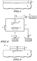
- FIG. 1 while not necessarily depicting any actual semiconductor device structure, serves to illustrate the application of the invention to the fabrication of a semiconductor device.
- Dielectric layer 12 can be one of several dielectric materials such as silicon dioxide, silicon nitride, oxynitride, and the like. Alternatively, dielectric layer 12 can be any composite material, such as, for example, an ONO layer comprised of individual layers of silicon oxide, silicon nitride, and silicon oxide. Additionally, dielectric layer 12 can be a ceramic dielectric material such as lead zirconium titanate (PZT), lead lanthanum zirconium titanate (PLZT), strontium titanate, barium titanate, and the like.
- PZT lead zirconium titanate
- PLAT lead lanthanum zirconium titanate
- strontium titanate barium titanate
- Metal oxide layer 14 can be formed by reactive sputter deposition or chemical vapor deposition of a noble metal.
- metal oxide layer 14 is ruthenium dioxide (RuO2).
- RuO2 is formed by DC reactive sputter deposition of Ru.
- the sputtering process is carried out in a low pressure oxygen and argon atmosphere using a pure ruthenium sputtering target.
- the argon and oxygen are present in the ratio of about 60 vol. percent argon and about 40 vol. percent oxygen.
- the sputtering process is initiated by applying about 400 watts of DC power at a system pressure of about 8 millitorr.
- the RuO2 film is sputter deposited to a thickness of about 50 nanometers and has a sheet resistance of about 120 to 150 ohms per square.
- Analysis by Rutherford backscattering spectroscopy (RBS) of the RuO2 film indicates the stoichiometric material composition to be 2.03 to 2.10 atoms of oxygen for every atom of ruthenium.
- metal oxide layer 14 can be formed by organometallic chemical vapor deposition of a noble metal followed by an oxidation step.
- Ru can be deposited by chemical vapor deposition of an organoruthenium complex such as bis(cyclopenta-dienyl) ruthenium (Ru (C5H5)2), triruthenium dodecacarbonyl (Ru3(CO)12), and the like, or alternatively, a halogenated compound such as ruthenium tetrachloride (RuCl4).
- organoruthenium complex such as bis(cyclopenta-dienyl) ruthenium (Ru (C5H5)2), triruthenium dodecacarbonyl (Ru3(CO)12), and the like, or alternatively, a halogenated compound such as ruthenium tetrachloride (RuCl4).
- the Ru film is then oxidized in an oxygen atmosphere at about 500 to 1000 ⁇ C.
- metal oxide layer 14 is etched in a parallel plate etching apparatus.
- the parallel plate etching apparatus is capable of controlling the internal atmospheric environment of the etch chamber, and applying RF power at 13.56 MHz to a pair of parallel opposing electrodes positioned within the etch chamber.
- the etching system is capable of controlling substrate temperature in a range from about 25 ⁇ C to 150 ⁇ C and has an RF power capacity ranging from 50 to 400 Watts.
- Many commercially available plasma etching systems have the necessary environmental control and RF power delivery capability to provide the aforementioned operating ranges.
- FIG. 2 One example of a plasma etching apparatus which can be used in practicing the invention is shown in FIG. 2.
- the apparatus comprises a vacuum chamber 20 which encloses a lower powered electrode 22 and an upper grounded electrode 24. Wafers to be etched are loaded into vacuum chamber 20 by means of an access door 26 and placed upon powered electrode 22. Processed wafers are removed from vacuum chamber 20 also by means of access door 26.
- electrodes 22 and 24 have generally planar surfaces and are parallel to one another. Both powered electrode 22 and grounded electrode 24 are electrically insulated from the walls of chamber 20. Grounded electrode 24 is adapted to dispense process gasses into the space between the two electrodes through a plurality of openings 28 in the lower surface of the electrode.
- a gas supply 30 and flow control valve 32 are coupled to electrode 24 in order to select and regulate the flow of gases to chamber 20.
- a vacuum system 34 is coupled through a pressure control valve 36 to chamber 20 to control the pressure therein and remove excess gaseous reaction products therefrom.
- the gases introduced to chamber 20 are energized by means of a 13.56 MHz power supply 38 coupled to electrode 22 through a matching network and blocking capacitor unit 40.
- the components described thus far are recognized by those skilled in the art as comprising a reactive ion etching (RIE) system. Gas introduced into the space between the two electrodes is excited to a high energy state by the RF energy emitted from power supply 38.
- RIE reactive ion etching
- semiconductor substrate 10, having metal oxide layer 14 thereon is placed on powered electrode 22.
- Door 26 is closed and vacuum system 34 removes the atmospheric gases from chamber 20.
- Flow control valve 32 is activated to introduce oxygen gas into chamber 20, and the internal pressure is adjusted to a level selected for optimum operation, preferably about 1 to 100 millitorr.
- Oxygen is introduced at a rate of about 10 to 100 sccm through flow control valve 32.
- Power supply 38 is activated imparting 50 to 400 watts of RF power at electrode 22 and igniting a plasma in the space between the two electrodes. Once a plasma is formed, an ion assisted chemical reaction takes place between the oxygen plasma and the metal oxide film. The plasma induced chemical reaction etches away the metal oxide layer 14 overlying dielectric layer 12.
- the temperature of substrate 12 is controlled to a temperature in the range of 25 to 50 ⁇ C.
- the reaction of oxygen with the metal oxide produces volatile reaction products which are removed by vacuum system 34.
- power supply 38 is shut off and chamber 20 is back-filled with an inert gas from gas supply 30 until the internal pressure is equalized to atmospheric pressure.
- Semiconductor substrate 10 is then removed from electrode 22 through door 26.
- etching apparatus such as a hexagonal bell-jar type reactor, a barrel reactor, a multi-chamber parallel plate reactor, and the like.
- an electron-cyclotron resonance type etching reactor can also be used.
- the particular style of etching system used will depend upon the specific etch characteristics that are desired. For example, in cases where the substrate is sensitive to applied voltage, an electron-cyclotron resonance reactor can be used.
- a barrel reactor can be used in cases where the metal oxide film is to be isotropically etched.
- the operating conditions such as RF power, vacuum pressure, and oxygen flow rate must be adjusted to optimize the etching process.
- FIG. 1 serves to illustrate the application of the invention to semiconductor device fabrication
- the invention contemplates the fabrication of more complex structures.
- the high resolution patterning capability of the invention enables the fabrication of a wide variety of integrated circuit components having a metal oxide conductor.
- One such component is a capacitor having metal oxide plates as illustrated in FIG. 3.
- a RuO2 bottom plate 50 overlies a doped region 52 formed in a semiconductor substrate 54.
- a dielectric layer 56 overlies bottom plate 50 and a RuO2 top plate 58 overlies dielectric 56.
- Bottom and top plates 50 and 58 and intermediate dielectric layer 56 form a thin-film capacitor 60.
- a barrier metal layer such as titanium nitride or titanium tungsten can be disposed between the substrate and the bottom capacitor plate.
- capacitor having RuO2 plates is depicted in FIG. 3; however, those skilled in the art will appreciate that the capacitor plates can be constructed from a different noble metal oxide having the general formula given above.
- the plates can be RhO2, IrO2, and the like.
- capacitor 60 is formed by first depositing a RuO2 layer using the DC reactive sputter deposition process previously described. After the first RuO2 layer is deposited, the layer is annealed and a dielectric layer is formed to overlie the first RuO2 layer.
- the dielectric layer can be one of a number of different dielectric materials commonly used in thin-film capacitors.
- the dielectric material can be similar to that of dielectric layer 12, e.g. silicon oxide or oxynitride and the like.
- the dielectric material can be one of the ceramic dielectric materials previously described, e.g. PZT, PLZT, strontium titanate, and barium titanate, and the like.
- capacitor 60 is a ferroelectric capacitor having a PLZT dielectric material.
- the PLZT layer is preferably formed by spin-coating a PLZT sol-gel solution onto substrate 54.
- the sol-gel solution includes complex molecules of lead, lanthanum, and zirconium titanate.
- substrate 54 is baked and sintered to form a crystalline PLZT perovskite.
- the PLZT layer can be formed by sputter deposition, or chemical vapor deposition, or the like.
- a second layer of RuO2 is deposited to overlie the PLZT layer.
- capacitor 60 To complete the fabrication of capacitor 60, a high resolution etch process is required to define the first and second RuO2 layers and the intermediate PLZT layer.
- Capacitor 60 must have the necessary geometric characteristics to be integrated into a complex semiconductor device such as an ultra-large-scale-integrated circuit.
- the fabrication of capacitor 60 requires that the etch process not only be capable of high resolution, but also be highly selective to underlying layers. For example, it is required that the etching of the first RuO2 layer proceed to the interface between the first RuO2 layer and substrate 54 without unduly etching away the surface of substrate 54.
- the formation of capacitor 60 additionally requires that the etch process not remove portions of the etching mask used to define the pattern of capacitor 60 on substrate 54. Furthermore, it is important that the etch process not degrade the dielectric characteristics of the PLZT layer by subjecting the PLZT layer to excessive voltages during the etching of any portion of capacitor 60.
- the process of the present invention is used to etch the RuO2 layers and the intermediate PLZT layer.
- an etch masking pattern is formed on the second RuO2 layer.
- a positive acting photoresist material which is resistant to being etched by an oxygen plasma, is used .
- a polyvinyl phenol is treated with hexamethyldisilazane to form a silylated resist which is then deposited onto substrate 54. The silylated resist is exposed and dry developed to form the desired pattern.
- a silicon implantation process can be used to impregnate polyvinyl phenol with silicon.
- a hard mask can be used.
- a material other than an organic photoresist can be used as an etch mask.
- a refractory metal, a refractory metal silicide, a refractory metal oxide, or a semiconductor, such as polysilicon can be used as an etch mask.
- Refractory metals include tungsten (W), titanium (Ti), molybdenum (Mo), and the like.
- Refractory metal oxides include titanium dioxide (TiO2), and tantalum pentoxide (Ta2O5), and the like.
- the second RuO2 layer is etched to form top plate 58 using the previously described oxygen plasma process. Since PLZT is substantially unreactive with oxygen, the oxygen plasma does not appreciably etch the underlying PLZT layer.
- the preferential etching of RuO2 is advantageous because an extended amount of time can be used, if necessary, to remove all of the exposed RuO2 layer. Over-etching is desirable in cases where the RuO2 layer is deposited over existing structures already in place on substrate 54. For example, regions where the RuO2 layer overlies steep edges require an extended etching time to remove all of the RuO2 overlying those edges.
- the PLZT layer is etched to form dielectric layer 56.
- a wet etching process is used to etch the PLZT layer.
- a solution of hydrogen fluoride and hydrogen chloride is maintained in a constant temperature bath.
- a photoresist pattern can be formed on top plate 58 to define a desired pattern.
- top plate 58 can be used as a hard mask for the PLZT etch process.
- Substrate 54 is immersed in the bath for a predetermined period of time removing all unprotected portions of the PLZT layer.
- a dry plasma etching process is used to etch the PLZT layer.
- the plasma etch can be carried out in a system similar to that illustrated in FIG. 2.
- the PLZT layer is plasma etched with halogenated etch gases such as a chlorinated gas at temperatures above about 150 ⁇ C.
- the first RuO2 layer is etched to form bottom plate 50.
- the previously described oxygen plasma etching process is used to etch the first RuO2 layer.
- the oxygen etch will also preferentially etch RuO2 deposited over silicon.
- a substantial over-etch can also be performed here to remove all portions of the first RuO2 layer.
- a ferroelectric capacitor is not limited to the formation of a ferroelectric capacitor.
- the process of the invention can be used to form a variety of integrated circuit components having a metal oxide layer.
- a conductive metal oxide can be used to form thin-film resistors.
- Thin-film resistors have widespread applications in electronic components such as sensors, resistor arrays, hybrid integrated circuits, and the like.
- a noble metal oxide is resistant to oxidation, such a material is advantageous in a semiconductor device structure or electronic component whenever an oxygen anneal must be performed during processing.
- a silicon substrate having a 50 nanometer thick RuO2 film to be etched was placed on the lower electrode of a parallel plate etching apparatus manufactured by Plasma-Therm Inc. of Kresson, New Jersey.
- the etch chamber was evacuated to a pressure of 45 millitorr and the substrate was heated to 35 ⁇ C.
- Oxygen gas was introduced at the rate of 50 standard cubic centimeters per minute and 200 watts of RF power was applied to the lower electrode at a frequency of 13.56 MHz.
- the application of the RF power to the lower electrode created a DC bias of about -516 volts at the electrode.
- the removal of the RuO2 film was monitored by periodically removing the substrate from the etch chamber and measuring the sheet resistance. Substantially all of the RuO2 was removed after an etching period of 10 minutes. The average etch rate of the RuO2 film was 57 angstroms per minute.
- a silicon substrate having a 50 nanometer thick RuO2 film to be etched was placed on the lower electrode of the apparatus described in Example I.
- the etch chamber was evacuated to a pressure of 45 millitorr and the substrate was heated to 35 ⁇ C.
- a combination of oxygen and tetrafluoromethane gas was introduced at the rate of 5 sccm oxygen and 45 sccm tetrafluoromethane.
- Two hundred watts of RF power was applied to the lower electrode at a frequency of 13.56 MHz.
- the application of the RF power to the lower electrode created a DC bias of about -478 volts at the electrode.
- the removal of the RuO2 film was monitored using the same method as in Example I.
- the average etch rate of the RuO2 film was about 2 angstroms per minute.
- a silicon substrate having a 50 nanometer thick RuO2 film to be etched was placed on a wafer tray and inserted into a barrel etching apparatus manufactured by Branson IPC, of Hayward, Ca.
- An initial 10 minute nitrogen plasma was formed by flowing about 500 sccm of nitrogen and applying about 500 watts of RF power.
- the pressure in the etch chamber was adjusted to a pressure of about 1 torr.
- oxygen gas was introduced at the rate of about 100 sccm and about 1000 watts of RF power was applied to the chamber at a frequency of 13.56 MHz.
- Substantially all of the RuO2 was removed after an etching period of 45 minutes.
- the etch results described in the Examples given above indicate that the oxygen plasma etching of an RuO2 film occurs by a plasma-assisted chemical reaction rather than by sputter etching.
- the etch results obtained with the barrel reactor described in Example III can only be obtained as a result of chemical etching. Because the substrate is at a voltage potential only slightly less than the plasma in a barrel-type reactor, during the etch, ions are not accelerated toward the substrate rapidly enough to sputter material from the substrate surface. Therefore, the etching mechanism is substantially a chemical reaction between activated oxygen atoms and the RuO2 material.
Landscapes
- Semiconductor Memories (AREA)
- Drying Of Semiconductors (AREA)
Applications Claiming Priority (2)
| Application Number | Priority Date | Filing Date | Title |
|---|---|---|---|
| US07/919,328 US5254217A (en) | 1992-07-27 | 1992-07-27 | Method for fabricating a semiconductor device having a conductive metal oxide |
| US919328 | 1992-07-27 |
Publications (2)
| Publication Number | Publication Date |
|---|---|
| EP0587990A2 true EP0587990A2 (fr) | 1994-03-23 |
| EP0587990A3 EP0587990A3 (en) | 1994-05-25 |
Family
ID=25441899
Family Applications (1)
| Application Number | Title | Priority Date | Filing Date |
|---|---|---|---|
| EP19930107990 Withdrawn EP0587990A3 (en) | 1992-07-27 | 1993-05-17 | Method for fabricating a semiconductive device having a conductive metal oxide |
Country Status (4)
| Country | Link |
|---|---|
| US (1) | US5254217A (fr) |
| EP (1) | EP0587990A3 (fr) |
| JP (1) | JPH0697121A (fr) |
| KR (1) | KR940002961A (fr) |
Cited By (5)
| Publication number | Priority date | Publication date | Assignee | Title |
|---|---|---|---|---|
| EP0740342A3 (fr) * | 1995-04-28 | 1997-10-29 | Rohm Co Ltd | Dispositif semi-conducteur et procédé d'interconnexion |
| EP0889506A3 (fr) * | 1997-07-03 | 1999-03-10 | Siemens Aktiengesellschaft | Procédé de gravure |
| EP0795896A3 (fr) * | 1996-03-15 | 1999-06-02 | ROHM Co., Ltd. | Procédé de gravure sèche |
| US5973342A (en) * | 1996-04-25 | 1999-10-26 | Rohm Co., Ltd. | Semiconductor device having an iridium electrode |
| WO2000001000A1 (fr) * | 1998-06-30 | 2000-01-06 | Matsushita Electronics Corporation | Procede de pulverisation cathodique en courant continu pour la fabrication d'electrodes lisses et de condensateurs ferroelectriques a film mince offrant une conservation de memoire amelioree |
Families Citing this family (50)
| Publication number | Priority date | Publication date | Assignee | Title |
|---|---|---|---|---|
| US5496437A (en) * | 1993-06-10 | 1996-03-05 | Ceram Incorporated | Reactive ion etching of lead zirconate titanate and ruthenium oxide thin films |
| US5439840A (en) * | 1993-08-02 | 1995-08-08 | Motorola, Inc. | Method of forming a nonvolatile random access memory capacitor cell having a metal-oxide dielectric |
| US5585776A (en) * | 1993-11-09 | 1996-12-17 | Research Foundation Of The State University Of Ny | Thin film resistors comprising ruthenium oxide |
| US5443688A (en) * | 1993-12-02 | 1995-08-22 | Raytheon Company | Method of manufacturing a ferroelectric device using a plasma etching process |
| JP4554631B2 (ja) * | 1994-01-13 | 2010-09-29 | ローム株式会社 | 誘電体キャパシタおよびその製造方法 |
| JP3460347B2 (ja) * | 1994-03-30 | 2003-10-27 | 松下電器産業株式会社 | 半導体装置の製造方法 |
| DE69529000T2 (de) * | 1994-03-30 | 2003-08-21 | Matsushita Electric Industrial Co., Ltd. | Verfahren zur Herstellung von Halbleitervorrichtungen mit eingebautem Kondensator |
| US5589284A (en) * | 1994-08-01 | 1996-12-31 | Texas Instruments Incorporated | Electrodes comprising conductive perovskite-seed layers for perovskite dielectrics |
| JP2956485B2 (ja) * | 1994-09-07 | 1999-10-04 | 日本電気株式会社 | 半導体装置の製造方法 |
| JP2703206B2 (ja) * | 1994-09-30 | 1998-01-26 | 三星電子株式会社 | 強誘電体キャパシタ及びその製造方法 |
| KR0147639B1 (ko) * | 1995-05-29 | 1998-08-01 | 김광호 | 고유전율 캐패시터의 하부전극 형성방법 |
| US5739049A (en) * | 1995-08-21 | 1998-04-14 | Hyundai Electronics Industries Co., Ltd. | Method for fabricating semiconductor device having a capacitor and a method of forming metal wiring on a semiconductor substrate |
| KR100200299B1 (ko) * | 1995-11-30 | 1999-06-15 | 김영환 | 반도체 소자 캐패시터 형성방법 |
| KR100413649B1 (ko) * | 1996-01-26 | 2004-04-28 | 마츠시타 덴끼 산교 가부시키가이샤 | 반도체장치의제조방법 |
| US5695815A (en) * | 1996-05-29 | 1997-12-09 | Micron Technology, Inc. | Metal carboxylate complexes for formation of metal-containing films on semiconductor devices |
| DE19631622A1 (de) * | 1996-08-05 | 1998-02-12 | Siemens Ag | Verfahren zum plasmaunterstützten anisotropen Ätzen von Metallen, Metalloxiden und deren Gemische |
| JP3512959B2 (ja) * | 1996-11-14 | 2004-03-31 | 株式会社東芝 | 半導体装置及びその製造方法 |
| DE19728473A1 (de) * | 1997-07-03 | 1999-01-07 | Siemens Ag | Strukturierungsverfahren |
| EP0895278A3 (fr) | 1997-08-01 | 2000-08-23 | Siemens Aktiengesellschaft | Procédé de structuration |
| JP3878724B2 (ja) * | 1997-10-14 | 2007-02-07 | 株式会社ルネサステクノロジ | 半導体集積回路装置およびその製造方法 |
| KR100458084B1 (ko) * | 1997-12-27 | 2005-06-07 | 주식회사 하이닉스반도체 | 누설전류가 감소된 하부전극을 갖는 강유전체 커패시터 형성 방법 |
| US6287975B1 (en) * | 1998-01-20 | 2001-09-11 | Tegal Corporation | Method for using a hard mask for critical dimension growth containment |
| KR100289389B1 (ko) * | 1998-03-05 | 2001-06-01 | 김영환 | 반도체소자의캐패시터제조방법 |
| US6277760B1 (en) * | 1998-06-26 | 2001-08-21 | Lg Electronics Inc. | Method for fabricating ferroelectric capacitor |
| US6537461B1 (en) * | 2000-04-24 | 2003-03-25 | Hitachi, Ltd. | Process for treating solid surface and substrate surface |
| SG79292A1 (en) | 1998-12-11 | 2001-03-20 | Hitachi Ltd | Semiconductor integrated circuit and its manufacturing method |
| US6399508B1 (en) | 1999-01-12 | 2002-06-04 | Applied Materials, Inc. | Method for metal etch using a dielectric hard mask |
| US6368518B1 (en) | 1999-08-25 | 2002-04-09 | Micron Technology, Inc. | Methods for removing rhodium- and iridium-containing films |
| US6265280B1 (en) * | 1999-11-29 | 2001-07-24 | Chartered Semiconductor Manufacturing, Inc. | Method for manufacturing a cylindrical semiconductor capacitor |
| US6492241B1 (en) * | 2000-04-10 | 2002-12-10 | Micron Technology, Inc. | Integrated capacitors fabricated with conductive metal oxides |
| KR100362906B1 (ko) * | 2000-04-22 | 2002-12-11 | 가부시키가이샤 히타치세이사쿠쇼 | 고체 표면, 기판 및 반도체 제조 장치의 처리 방법 및이들을 이용한 반도체 장치의 제조 방법 |
| US6455326B1 (en) * | 2000-05-15 | 2002-09-24 | Ramtron International Corporation | Enhanced process capability for sputtered ferroelectric films using low frequency pulsed DC and RF power supplies |
| DE10038877A1 (de) * | 2000-08-09 | 2002-02-28 | Infineon Technologies Ag | Speicherzelle und Herstellungsverfahren |
| US6730984B1 (en) * | 2000-11-14 | 2004-05-04 | International Business Machines Corporation | Increasing an electrical resistance of a resistor by oxidation or nitridization |
| US6709609B2 (en) * | 2000-12-22 | 2004-03-23 | Applied Materials Inc. | Plasma heating of a substrate with subsequent high temperature etching |
| US6692648B2 (en) * | 2000-12-22 | 2004-02-17 | Applied Materials Inc. | Method of plasma heating and etching a substrate |
| US6495413B2 (en) | 2001-02-28 | 2002-12-17 | Ramtron International Corporation | Structure for masking integrated capacitors of particular utility for ferroelectric memory integrated circuits |
| JP2002280360A (ja) | 2001-03-16 | 2002-09-27 | Nec Corp | 半導体装置の製造方法 |
| US6423592B1 (en) | 2001-06-26 | 2002-07-23 | Ramtron International Corporation | PZT layer as a temporary encapsulation and hard mask for a ferroelectric capacitor |
| US6762090B2 (en) * | 2001-09-13 | 2004-07-13 | Hynix Semiconductor Inc. | Method for fabricating a capacitor |
| US7049237B2 (en) | 2001-12-21 | 2006-05-23 | Micron Technology, Inc. | Methods for planarization of Group VIII metal-containing surfaces using oxidizing gases |
| US20030119316A1 (en) * | 2001-12-21 | 2003-06-26 | Micron Technology, Inc. | Methods for planarization of group VIII metal-containing surfaces using oxidizing agents |
| US6730592B2 (en) | 2001-12-21 | 2004-05-04 | Micron Technology, Inc. | Methods for planarization of metal-containing surfaces using halogens and halide salts |
| US6884723B2 (en) * | 2001-12-21 | 2005-04-26 | Micron Technology, Inc. | Methods for planarization of group VIII metal-containing surfaces using complexing agents |
| US7121926B2 (en) | 2001-12-21 | 2006-10-17 | Micron Technology, Inc. | Methods for planarization of group VIII metal-containing surfaces using a fixed abrasive article |
| US6686236B2 (en) * | 2001-12-21 | 2004-02-03 | Texas Instruments Incorporated | Methods of preventing reduction of IrOx during PZT formation by metalorganic chemical vapor deposition or other processing |
| DE10255841A1 (de) * | 2002-11-29 | 2004-06-17 | Infineon Technologies Ag | Kondensator mit ruthenhaltigen Elektroden |
| US20060073613A1 (en) * | 2004-09-29 | 2006-04-06 | Sanjeev Aggarwal | Ferroelectric memory cells and methods for fabricating ferroelectric memory cells and ferroelectric capacitors thereof |
| KR100858082B1 (ko) * | 2006-10-17 | 2008-09-10 | 삼성전자주식회사 | 니켈 산화물층의 식각 방법 |
| US9016236B2 (en) * | 2008-08-04 | 2015-04-28 | International Business Machines Corporation | Method and apparatus for angular high density plasma chemical vapor deposition |
Family Cites Families (11)
| Publication number | Priority date | Publication date | Assignee | Title |
|---|---|---|---|---|
| US3698078A (en) * | 1969-12-22 | 1972-10-17 | Gen Electric | Diode array storage system having a self-registered target and method of forming |
| DD289438A7 (de) * | 1978-01-16 | 1991-05-02 | Schiffselektronik,De | Einrichtung zur beeinflussung der stroemung an akustischen strahlern bzw. empfaengern |
| US4357369A (en) * | 1981-11-10 | 1982-11-02 | Rca Corporation | Method of plasma etching a substrate |
| JPS6057511B2 (ja) * | 1981-11-25 | 1985-12-16 | 富士通株式会社 | 酸化クロムCr↓2O↓3のドライエツチング法 |
| JP2542608B2 (ja) * | 1987-03-09 | 1996-10-09 | 住友電気工業株式会社 | ダイヤモンド半導体のエツチング方法 |
| JP2679148B2 (ja) * | 1988-09-09 | 1997-11-19 | 松下電器産業株式会社 | 酸化ルテニウム系薄膜のエッチング方法 |
| JP2679201B2 (ja) * | 1988-12-28 | 1997-11-19 | 松下電器産業株式会社 | 酸化ルテニウム系薄膜のエッチング方法 |
| US5003428A (en) * | 1989-07-17 | 1991-03-26 | National Semiconductor Corporation | Electrodes for ceramic oxide capacitors |
| US4982309A (en) * | 1989-07-17 | 1991-01-01 | National Semiconductor Corporation | Electrodes for electrical ceramic oxide devices |
| US5118382A (en) * | 1990-08-10 | 1992-06-02 | Ibm Corporation | Elimination of etch stop undercut |
| US5139974A (en) * | 1991-01-25 | 1992-08-18 | Micron Technology, Inc. | Semiconductor manufacturing process for decreasing the optical refelctivity of a metal layer |
-
1992
- 1992-07-27 US US07/919,328 patent/US5254217A/en not_active Expired - Lifetime
-
1993
- 1993-05-17 EP EP19930107990 patent/EP0587990A3/en not_active Withdrawn
- 1993-06-18 KR KR1019930011163A patent/KR940002961A/ko not_active Withdrawn
- 1993-07-26 JP JP5203645A patent/JPH0697121A/ja active Pending
Cited By (7)
| Publication number | Priority date | Publication date | Assignee | Title |
|---|---|---|---|---|
| EP0740342A3 (fr) * | 1995-04-28 | 1997-10-29 | Rohm Co Ltd | Dispositif semi-conducteur et procédé d'interconnexion |
| US5841160A (en) * | 1995-04-28 | 1998-11-24 | Rohm Co., Ltd. | Semiconductor device having a capacitor electrode made of iridium |
| EP0795896A3 (fr) * | 1996-03-15 | 1999-06-02 | ROHM Co., Ltd. | Procédé de gravure sèche |
| US5973342A (en) * | 1996-04-25 | 1999-10-26 | Rohm Co., Ltd. | Semiconductor device having an iridium electrode |
| EP0889506A3 (fr) * | 1997-07-03 | 1999-03-10 | Siemens Aktiengesellschaft | Procédé de gravure |
| WO2000001000A1 (fr) * | 1998-06-30 | 2000-01-06 | Matsushita Electronics Corporation | Procede de pulverisation cathodique en courant continu pour la fabrication d'electrodes lisses et de condensateurs ferroelectriques a film mince offrant une conservation de memoire amelioree |
| US6541375B1 (en) | 1998-06-30 | 2003-04-01 | Matsushita Electric Industrial Co., Ltd. | DC sputtering process for making smooth electrodes and thin film ferroelectric capacitors having improved memory retention |
Also Published As
| Publication number | Publication date |
|---|---|
| US5254217A (en) | 1993-10-19 |
| KR940002961A (ko) | 1994-02-19 |
| JPH0697121A (ja) | 1994-04-08 |
| EP0587990A3 (en) | 1994-05-25 |
Similar Documents
| Publication | Publication Date | Title |
|---|---|---|
| US5254217A (en) | Method for fabricating a semiconductor device having a conductive metal oxide | |
| US5258093A (en) | Procss for fabricating a ferroelectric capacitor in a semiconductor device | |
| JP3114916B2 (ja) | 層状構造酸化物薄膜の乾式エッチング方法 | |
| KR100269314B1 (ko) | 플라즈마처리를이용한반도체장치의커패시터제조방법 | |
| US6475854B2 (en) | Method of forming metal electrodes | |
| US6338994B1 (en) | Semiconductor device and method of fabricating thereof | |
| US6498097B1 (en) | Apparatus and method of forming preferred orientation-controlled platinum film using oxygen | |
| EP0726600A2 (fr) | Méthode de formation d'une structure pour DRAM et structure ainsi formée | |
| US6432767B2 (en) | Method of fabricating semiconductor device | |
| US20030077843A1 (en) | Method of etching conductive layers for capacitor and semiconductor device fabrication | |
| US20020117701A1 (en) | Process and structure for masking integrated capacitors of particular utility for ferroelectric memory integrated circuits | |
| US6296777B1 (en) | Structuring process | |
| KR20020093049A (ko) | 납 지르코늄 티타네이트 및 바륨 스트론튬 티타네이트를패터닝하는 방법 | |
| WO1996027208A1 (fr) | Procede de formation d'une structure par redeposition | |
| US20020076936A1 (en) | Method of fabricating semiconductor integrated circuit device and the semiconductor integrated circuit device | |
| US20030047532A1 (en) | Method of etching ferroelectric layers | |
| KR100289389B1 (ko) | 반도체소자의캐패시터제조방법 | |
| US6372519B1 (en) | In-situ formation of metal oxide and ferroelectic oxide films | |
| KR19980070737A (ko) | 기판상에 귀금속 함유 구조물을 만들기 위한 방법 및 상기구조물을 가진 반도체 소자 | |
| KR100474589B1 (ko) | 캐패시터제조방법 | |
| US6783996B2 (en) | Capacitor of semiconductor device and fabrication method thereof | |
| JPH10163447A (ja) | 薄膜キャパシタ、その製造方法および電極の加工方法 | |
| KR100461506B1 (ko) | 박막 식각 방법 및 이를 이용한 반도체 소자의 트랜지스터및 캐패시터 제조 방법 | |
| US7329548B2 (en) | Integration processes for fabricating a conductive metal oxide gate ferroelectric memory transistor | |
| KR100255660B1 (ko) | 이리듐막의 식각 방법 |
Legal Events
| Date | Code | Title | Description |
|---|---|---|---|
| PUAI | Public reference made under article 153(3) epc to a published international application that has entered the european phase |
Free format text: ORIGINAL CODE: 0009012 |
|
| AK | Designated contracting states |
Kind code of ref document: A2 Designated state(s): DE FR GB IT |
|
| PUAL | Search report despatched |
Free format text: ORIGINAL CODE: 0009013 |
|
| AK | Designated contracting states |
Kind code of ref document: A3 Designated state(s): DE FR GB IT |
|
| 17P | Request for examination filed |
Effective date: 19941125 |
|
| 17Q | First examination report despatched |
Effective date: 19941229 |
|
| 18D | Application deemed to be withdrawn |
Effective date: 19980402 |