EP0588492A1 - Film épais et flexible de photorésistance positive ayant un haut facteur de forme - Google Patents
Film épais et flexible de photorésistance positive ayant un haut facteur de forme Download PDFInfo
- Publication number
- EP0588492A1 EP0588492A1 EP93306421A EP93306421A EP0588492A1 EP 0588492 A1 EP0588492 A1 EP 0588492A1 EP 93306421 A EP93306421 A EP 93306421A EP 93306421 A EP93306421 A EP 93306421A EP 0588492 A1 EP0588492 A1 EP 0588492A1
- Authority
- EP
- European Patent Office
- Prior art keywords
- film
- substrate
- anhydride
- photoresist
- thickness
- Prior art date
- Legal status (The legal status is an assumption and is not a legal conclusion. Google has not performed a legal analysis and makes no representation as to the accuracy of the status listed.)
- Withdrawn
Links
- 229920002120 photoresistant polymer Polymers 0.000 title claims abstract description 38
- 239000000203 mixture Substances 0.000 claims abstract description 24
- 239000000758 substrate Substances 0.000 claims abstract description 23
- 229920001577 copolymer Polymers 0.000 claims abstract description 18
- 229920003986 novolac Polymers 0.000 claims abstract description 16
- 239000003504 photosensitizing agent Substances 0.000 claims abstract description 15
- -1 alkyl vinyl ether Chemical compound 0.000 claims abstract description 9
- 239000002356 single layer Substances 0.000 claims abstract description 9
- 150000008064 anhydrides Chemical class 0.000 claims abstract description 8
- 150000002148 esters Chemical class 0.000 claims abstract description 6
- 150000001990 dicarboxylic acid derivatives Chemical class 0.000 claims abstract 4
- 238000000034 method Methods 0.000 claims description 30
- 239000002904 solvent Substances 0.000 claims description 11
- 239000000463 material Substances 0.000 claims description 7
- 239000010410 layer Substances 0.000 claims description 6
- 230000005855 radiation Effects 0.000 claims description 5
- XJRBAMWJDBPFIM-UHFFFAOYSA-N methyl vinyl ether Chemical group COC=C XJRBAMWJDBPFIM-UHFFFAOYSA-N 0.000 claims description 3
- 238000002360 preparation method Methods 0.000 claims description 3
- QYKIQEUNHZKYBP-UHFFFAOYSA-N Vinyl ether Chemical compound C=COC=C QYKIQEUNHZKYBP-UHFFFAOYSA-N 0.000 claims description 2
- 239000002253 acid Substances 0.000 claims description 2
- 238000000151 deposition Methods 0.000 claims description 2
- 238000001035 drying Methods 0.000 claims description 2
- RTZKZFJDLAIYFH-UHFFFAOYSA-N Diethyl ether Chemical compound CCOCC RTZKZFJDLAIYFH-UHFFFAOYSA-N 0.000 claims 2
- 229920002554 vinyl polymer Polymers 0.000 claims 1
- 239000000243 solution Substances 0.000 description 15
- LZCLXQDLBQLTDK-UHFFFAOYSA-N ethyl 2-hydroxypropanoate Chemical compound CCOC(=O)C(C)O LZCLXQDLBQLTDK-UHFFFAOYSA-N 0.000 description 10
- IWDCLRJOBJJRNH-UHFFFAOYSA-N p-cresol Chemical compound CC1=CC=C(O)C=C1 IWDCLRJOBJJRNH-UHFFFAOYSA-N 0.000 description 10
- 235000012431 wafers Nutrition 0.000 description 10
- DKPFZGUDAPQIHT-UHFFFAOYSA-N Butyl acetate Natural products CCCCOC(C)=O DKPFZGUDAPQIHT-UHFFFAOYSA-N 0.000 description 9
- WSFSSNUMVMOOMR-UHFFFAOYSA-N Formaldehyde Chemical compound O=C WSFSSNUMVMOOMR-UHFFFAOYSA-N 0.000 description 9
- 239000011248 coating agent Substances 0.000 description 9
- 238000000576 coating method Methods 0.000 description 9
- XUIMIQQOPSSXEZ-UHFFFAOYSA-N Silicon Chemical compound [Si] XUIMIQQOPSSXEZ-UHFFFAOYSA-N 0.000 description 7
- 229910052710 silicon Inorganic materials 0.000 description 7
- 239000010703 silicon Substances 0.000 description 7
- 125000000217 alkyl group Chemical group 0.000 description 6
- 229910000679 solder Inorganic materials 0.000 description 6
- 229940116333 ethyl lactate Drugs 0.000 description 5
- 238000010943 off-gassing Methods 0.000 description 5
- 239000007787 solid Substances 0.000 description 5
- 230000000694 effects Effects 0.000 description 4
- RLSSMJSEOOYNOY-UHFFFAOYSA-N m-cresol Chemical compound CC1=CC=CC(O)=C1 RLSSMJSEOOYNOY-UHFFFAOYSA-N 0.000 description 4
- 238000007747 plating Methods 0.000 description 4
- MUBZPKHOEPUJKR-UHFFFAOYSA-N Oxalic acid Chemical compound OC(=O)C(O)=O MUBZPKHOEPUJKR-UHFFFAOYSA-N 0.000 description 3
- KWYUFKZDYYNOTN-UHFFFAOYSA-M Potassium hydroxide Chemical compound [OH-].[K+] KWYUFKZDYYNOTN-UHFFFAOYSA-M 0.000 description 3
- DNIAPMSPPWPWGF-UHFFFAOYSA-N Propylene glycol Chemical compound CC(O)CO DNIAPMSPPWPWGF-UHFFFAOYSA-N 0.000 description 3
- 238000007334 copolymerization reaction Methods 0.000 description 3
- 238000005336 cracking Methods 0.000 description 3
- 150000001991 dicarboxylic acids Chemical class 0.000 description 3
- FPYJFEHAWHCUMM-UHFFFAOYSA-N maleic anhydride Chemical compound O=C1OC(=O)C=C1 FPYJFEHAWHCUMM-UHFFFAOYSA-N 0.000 description 3
- 238000004519 manufacturing process Methods 0.000 description 3
- 239000004014 plasticizer Substances 0.000 description 3
- 238000004528 spin coating Methods 0.000 description 3
- VZCYOOQTPOCHFL-UHFFFAOYSA-N trans-butenedioic acid Natural products OC(=O)C=CC(O)=O VZCYOOQTPOCHFL-UHFFFAOYSA-N 0.000 description 3
- DHKHKXVYLBGOIT-UHFFFAOYSA-N 1,1-Diethoxyethane Chemical compound CCOC(C)OCC DHKHKXVYLBGOIT-UHFFFAOYSA-N 0.000 description 2
- WTQZSMDDRMKJRI-UHFFFAOYSA-N 4-diazoniophenolate Chemical compound [O-]C1=CC=C([N+]#N)C=C1 WTQZSMDDRMKJRI-UHFFFAOYSA-N 0.000 description 2
- QTBSBXVTEAMEQO-UHFFFAOYSA-M Acetate Chemical compound CC([O-])=O QTBSBXVTEAMEQO-UHFFFAOYSA-M 0.000 description 2
- RYGMFSIKBFXOCR-UHFFFAOYSA-N Copper Chemical compound [Cu] RYGMFSIKBFXOCR-UHFFFAOYSA-N 0.000 description 2
- VZCYOOQTPOCHFL-OWOJBTEDSA-N Fumaric acid Chemical compound OC(=O)\C=C\C(O)=O VZCYOOQTPOCHFL-OWOJBTEDSA-N 0.000 description 2
- VEXZGXHMUGYJMC-UHFFFAOYSA-N Hydrochloric acid Chemical compound Cl VEXZGXHMUGYJMC-UHFFFAOYSA-N 0.000 description 2
- OFOBLEOULBTSOW-UHFFFAOYSA-N Propanedioic acid Natural products OC(=O)CC(O)=O OFOBLEOULBTSOW-UHFFFAOYSA-N 0.000 description 2
- VYPSYNLAJGMNEJ-UHFFFAOYSA-N Silicium dioxide Chemical compound O=[Si]=O VYPSYNLAJGMNEJ-UHFFFAOYSA-N 0.000 description 2
- 239000011354 acetal resin Substances 0.000 description 2
- 229910052802 copper Inorganic materials 0.000 description 2
- 239000010949 copper Substances 0.000 description 2
- 150000002170 ethers Chemical class 0.000 description 2
- 125000001495 ethyl group Chemical group [H]C([H])([H])C([H])([H])* 0.000 description 2
- XLLIQLLCWZCATF-UHFFFAOYSA-N ethylene glycol monomethyl ether acetate Natural products COCCOC(C)=O XLLIQLLCWZCATF-UHFFFAOYSA-N 0.000 description 2
- PCHJSUWPFVWCPO-UHFFFAOYSA-N gold Chemical compound [Au] PCHJSUWPFVWCPO-UHFFFAOYSA-N 0.000 description 2
- 239000010931 gold Substances 0.000 description 2
- 229910052737 gold Inorganic materials 0.000 description 2
- 238000005304 joining Methods 0.000 description 2
- VZCYOOQTPOCHFL-UPHRSURJSA-N maleic acid Chemical compound OC(=O)\C=C/C(O)=O VZCYOOQTPOCHFL-UPHRSURJSA-N 0.000 description 2
- 239000011976 maleic acid Substances 0.000 description 2
- 238000005259 measurement Methods 0.000 description 2
- 238000004806 packaging method and process Methods 0.000 description 2
- 229920001568 phenolic resin Polymers 0.000 description 2
- 239000005011 phenolic resin Substances 0.000 description 2
- 229920006324 polyoxymethylene Polymers 0.000 description 2
- 239000004065 semiconductor Substances 0.000 description 2
- 239000007921 spray Substances 0.000 description 2
- 238000005507 spraying Methods 0.000 description 2
- WGTYBPLFGIVFAS-UHFFFAOYSA-M tetramethylammonium hydroxide Chemical compound [OH-].C[N+](C)(C)C WGTYBPLFGIVFAS-UHFFFAOYSA-M 0.000 description 2
- WOAHJDHKFWSLKE-UHFFFAOYSA-N 1,2-benzoquinone Chemical compound O=C1C=CC=CC1=O WOAHJDHKFWSLKE-UHFFFAOYSA-N 0.000 description 1
- WJQOZHYUIDYNHM-UHFFFAOYSA-N 2-tert-Butylphenol Chemical compound CC(C)(C)C1=CC=CC=C1O WJQOZHYUIDYNHM-UHFFFAOYSA-N 0.000 description 1
- ZCILGMFPJBRCNO-UHFFFAOYSA-N 4-phenyl-2H-benzotriazol-5-ol Chemical class OC1=CC=C2NN=NC2=C1C1=CC=CC=C1 ZCILGMFPJBRCNO-UHFFFAOYSA-N 0.000 description 1
- VHUUQVKOLVNVRT-UHFFFAOYSA-N Ammonium hydroxide Chemical compound [NH4+].[OH-] VHUUQVKOLVNVRT-UHFFFAOYSA-N 0.000 description 1
- VEXZGXHMUGYJMC-UHFFFAOYSA-M Chloride anion Chemical compound [Cl-] VEXZGXHMUGYJMC-UHFFFAOYSA-M 0.000 description 1
- CTQNGGLPUBDAKN-UHFFFAOYSA-N O-Xylene Chemical compound CC1=CC=CC=C1C CTQNGGLPUBDAKN-UHFFFAOYSA-N 0.000 description 1
- ISWSIDIOOBJBQZ-UHFFFAOYSA-N Phenol Chemical compound OC1=CC=CC=C1 ISWSIDIOOBJBQZ-UHFFFAOYSA-N 0.000 description 1
- 239000004642 Polyimide Substances 0.000 description 1
- 239000004743 Polypropylene Substances 0.000 description 1
- 229910052581 Si3N4 Inorganic materials 0.000 description 1
- ZOIORXHNWRGPMV-UHFFFAOYSA-N acetic acid;zinc Chemical compound [Zn].CC(O)=O.CC(O)=O ZOIORXHNWRGPMV-UHFFFAOYSA-N 0.000 description 1
- 230000002378 acidificating effect Effects 0.000 description 1
- 238000013019 agitation Methods 0.000 description 1
- 150000008044 alkali metal hydroxides Chemical class 0.000 description 1
- 239000012670 alkaline solution Substances 0.000 description 1
- 125000005907 alkyl ester group Chemical group 0.000 description 1
- 150000005215 alkyl ethers Chemical class 0.000 description 1
- 229910052782 aluminium Inorganic materials 0.000 description 1
- XAGFODPZIPBFFR-UHFFFAOYSA-N aluminium Chemical compound [Al] XAGFODPZIPBFFR-UHFFFAOYSA-N 0.000 description 1
- 239000000908 ammonium hydroxide Substances 0.000 description 1
- 239000007864 aqueous solution Substances 0.000 description 1
- 239000002585 base Substances 0.000 description 1
- KGBXLFKZBHKPEV-UHFFFAOYSA-N boric acid Chemical compound OB(O)O KGBXLFKZBHKPEV-UHFFFAOYSA-N 0.000 description 1
- 239000004327 boric acid Substances 0.000 description 1
- 125000000484 butyl group Chemical group [H]C([*])([H])C([H])([H])C([H])([H])C([H])([H])[H] 0.000 description 1
- 125000004432 carbon atom Chemical group C* 0.000 description 1
- 230000015556 catabolic process Effects 0.000 description 1
- 239000003054 catalyst Substances 0.000 description 1
- 239000000919 ceramic Substances 0.000 description 1
- 238000009833 condensation Methods 0.000 description 1
- 230000005494 condensation Effects 0.000 description 1
- 239000004020 conductor Substances 0.000 description 1
- 229940118056 cresol / formaldehyde Drugs 0.000 description 1
- 230000003247 decreasing effect Effects 0.000 description 1
- 238000006731 degradation reaction Methods 0.000 description 1
- 239000003989 dielectric material Substances 0.000 description 1
- 238000010790 dilution Methods 0.000 description 1
- 239000012895 dilution Substances 0.000 description 1
- 238000007598 dipping method Methods 0.000 description 1
- 238000004090 dissolution Methods 0.000 description 1
- 238000005516 engineering process Methods 0.000 description 1
- 238000001704 evaporation Methods 0.000 description 1
- 230000008020 evaporation Effects 0.000 description 1
- 238000009472 formulation Methods 0.000 description 1
- 239000001530 fumaric acid Substances 0.000 description 1
- FUZZWVXGSFPDMH-UHFFFAOYSA-N hexanoic acid Chemical compound CCCCCC(O)=O FUZZWVXGSFPDMH-UHFFFAOYSA-N 0.000 description 1
- 235000011167 hydrochloric acid Nutrition 0.000 description 1
- 230000007062 hydrolysis Effects 0.000 description 1
- 238000006460 hydrolysis reaction Methods 0.000 description 1
- 238000007654 immersion Methods 0.000 description 1
- 239000011229 interlayer Substances 0.000 description 1
- UEGPKNKPLBYCNK-UHFFFAOYSA-L magnesium acetate Chemical compound [Mg+2].CC([O-])=O.CC([O-])=O UEGPKNKPLBYCNK-UHFFFAOYSA-L 0.000 description 1
- 239000011654 magnesium acetate Substances 0.000 description 1
- 229940069446 magnesium acetate Drugs 0.000 description 1
- 235000011285 magnesium acetate Nutrition 0.000 description 1
- 125000002496 methyl group Chemical group [H]C([H])([H])* 0.000 description 1
- 238000002156 mixing Methods 0.000 description 1
- 239000000178 monomer Substances 0.000 description 1
- 235000006408 oxalic acid Nutrition 0.000 description 1
- 239000002245 particle Substances 0.000 description 1
- 230000037361 pathway Effects 0.000 description 1
- 238000000059 patterning Methods 0.000 description 1
- 229920003023 plastic Polymers 0.000 description 1
- 239000004033 plastic Substances 0.000 description 1
- 229910021420 polycrystalline silicon Inorganic materials 0.000 description 1
- 229920001721 polyimide Polymers 0.000 description 1
- 229920001155 polypropylene Polymers 0.000 description 1
- 229920005591 polysilicon Polymers 0.000 description 1
- 239000011148 porous material Substances 0.000 description 1
- 125000001436 propyl group Chemical group [H]C([*])([H])C([H])([H])C([H])([H])[H] 0.000 description 1
- LLHKCFNBLRBOGN-UHFFFAOYSA-N propylene glycol methyl ether acetate Chemical compound COCC(C)OC(C)=O LLHKCFNBLRBOGN-UHFFFAOYSA-N 0.000 description 1
- 238000005086 pumping Methods 0.000 description 1
- 239000011541 reaction mixture Substances 0.000 description 1
- 229920005989 resin Polymers 0.000 description 1
- 239000011347 resin Substances 0.000 description 1
- 238000001878 scanning electron micrograph Methods 0.000 description 1
- 238000005204 segregation Methods 0.000 description 1
- 239000000377 silicon dioxide Substances 0.000 description 1
- 235000012239 silicon dioxide Nutrition 0.000 description 1
- HQVNEWCFYHHQES-UHFFFAOYSA-N silicon nitride Chemical compound N12[Si]34N5[Si]62N3[Si]51N64 HQVNEWCFYHHQES-UHFFFAOYSA-N 0.000 description 1
- 239000011877 solvent mixture Substances 0.000 description 1
- 238000009987 spinning Methods 0.000 description 1
- 229910052715 tantalum Inorganic materials 0.000 description 1
- GUVRBAGPIYLISA-UHFFFAOYSA-N tantalum atom Chemical compound [Ta] GUVRBAGPIYLISA-UHFFFAOYSA-N 0.000 description 1
- XLYOFNOQVPJJNP-UHFFFAOYSA-N water Substances O XLYOFNOQVPJJNP-UHFFFAOYSA-N 0.000 description 1
- 239000008096 xylene Substances 0.000 description 1
- 239000004246 zinc acetate Substances 0.000 description 1
- 235000013904 zinc acetate Nutrition 0.000 description 1
Images


Classifications
-
- G—PHYSICS
- G03—PHOTOGRAPHY; CINEMATOGRAPHY; ANALOGOUS TECHNIQUES USING WAVES OTHER THAN OPTICAL WAVES; ELECTROGRAPHY; HOLOGRAPHY
- G03F—PHOTOMECHANICAL PRODUCTION OF TEXTURED OR PATTERNED SURFACES, e.g. FOR PRINTING, FOR PROCESSING OF SEMICONDUCTOR DEVICES; MATERIALS THEREFOR; ORIGINALS THEREFOR; APPARATUS SPECIALLY ADAPTED THEREFOR
- G03F7/00—Photomechanical, e.g. photolithographic, production of textured or patterned surfaces, e.g. printing surfaces; Materials therefor, e.g. comprising photoresists; Apparatus specially adapted therefor
- G03F7/16—Coating processes; Apparatus therefor
-
- G—PHYSICS
- G03—PHOTOGRAPHY; CINEMATOGRAPHY; ANALOGOUS TECHNIQUES USING WAVES OTHER THAN OPTICAL WAVES; ELECTROGRAPHY; HOLOGRAPHY
- G03F—PHOTOMECHANICAL PRODUCTION OF TEXTURED OR PATTERNED SURFACES, e.g. FOR PRINTING, FOR PROCESSING OF SEMICONDUCTOR DEVICES; MATERIALS THEREFOR; ORIGINALS THEREFOR; APPARATUS SPECIALLY ADAPTED THEREFOR
- G03F7/00—Photomechanical, e.g. photolithographic, production of textured or patterned surfaces, e.g. printing surfaces; Materials therefor, e.g. comprising photoresists; Apparatus specially adapted therefor
- G03F7/004—Photosensitive materials
-
- G—PHYSICS
- G03—PHOTOGRAPHY; CINEMATOGRAPHY; ANALOGOUS TECHNIQUES USING WAVES OTHER THAN OPTICAL WAVES; ELECTROGRAPHY; HOLOGRAPHY
- G03F—PHOTOMECHANICAL PRODUCTION OF TEXTURED OR PATTERNED SURFACES, e.g. FOR PRINTING, FOR PROCESSING OF SEMICONDUCTOR DEVICES; MATERIALS THEREFOR; ORIGINALS THEREFOR; APPARATUS SPECIALLY ADAPTED THEREFOR
- G03F7/00—Photomechanical, e.g. photolithographic, production of textured or patterned surfaces, e.g. printing surfaces; Materials therefor, e.g. comprising photoresists; Apparatus specially adapted therefor
- G03F7/004—Photosensitive materials
- G03F7/022—Quinonediazides
- G03F7/023—Macromolecular quinonediazides; Macromolecular additives, e.g. binders
- G03F7/0233—Macromolecular quinonediazides; Macromolecular additives, e.g. binders characterised by the polymeric binders or the macromolecular additives other than the macromolecular quinonediazides
Definitions
- This invention relates to a positive working photoresist having a superior photospeed and a high contrast capability. It relates particularly to a composition which is capable of forming a single layer, 100 ⁇ thick resist. More particularly, it relates to a flexible thick film resist having several uses, the bonding of semiconductor chips in the manufacture of multi-chip modules being one of the more notable ones.
- Layers of positive working photoresists up to about 100 ⁇ thick and the resultant high aspect ratios are of increasing interest for a multitude of applications.
- the electric conductance of magnetic head interconnection circuitry fabricated by the photoresist technique is increased by the increased thickness of the copper or other conductor which is plated on the substrate according to patterns outlined in the photoimaged and developed thick film resist.
- MCM packaging is attractive to the IC industry in part because the close grouping of the die affords shorter pathways between chips and the consequent shorter time for the passage of electrical signals.
- the solder bump (C4) flip chip process is uniquely suited to the requirements of high density VLSI chips, i.e., 500-1000 I/O's per chip.
- the solder bump process requires a photoresist that can be coated on a substrate in one application to a thickness of from 50 to 60w.
- the film must have a uniform thickness and the sidewalls of the vias in the relief images developed therein must be substantially vertical.
- the typical thick film resists exhibit very poor thickness uniformity and are susceptible to outgassing and cracking when the thickness is greater than about 5p.
- a 100 ⁇ thick coat of the known resists could not be achieved in a single coating step.
- the pumping, coating, baking, exposing, and developing of the thick film resist candidate for the solder bump process must fit the standard semiconductor process and be compatible with the equipment. No resist currently on the market meets all of the requirements of the solder bump process.
- solder bump flip chip process is used as the interconnect technique in MCM manufacturing
- conventional photosensitive polyimides must be used as the dielectric material to be patterned for use as interlayers in MCM's. High thermal resistance is required.
- the photoresist required for patterning the dielectric for MCM manufacturing may be based on novolac resins. It must have the same properties as those required for the solder bump process but the film thickness need only be from about 7 to about 25w.
- a photoresist comprising a novolac resin, a quinone diazide photosensitizer, and a propylene glycol alkylether acetate are improved by the addition of a plasticizer such as polypropylene acetal resin according to U. S. Patent 5,066,561.
- a plasticizer such as polypropylene acetal resin according to U. S. Patent 5,066,561.
- a smooth film of uniform thickness is said to result.
- Formvar 5/95 E acetal resin Monsanto
- a substituted hydroxy phenyl benzotriazole at concentrations up to 2 weight percent and t-butylphenol at up to 1% by weight were not effective for the purposes of this invention.
- a positive photoresist composition comprising a novolac resin, a photosensitizer, a copolymer of an alkyl vinyl ether and an anhydride-forming unsaturated dicarboxylic acid, and a solvent in an amount sufficient to form a film having a dry thickness of from greater than 5p to about 100w, drying the layer, exposing the film imagewise to actinic radiation, baking the exposed film, and developing it.
- novolac resins The preparation of novolac resins is well known in the art. Phenol and/or alkyl phenols are condensed with formaldehyde at temperatures of from 100 to 190°C for several hours in the presence of a acidic catalyst such as hydrochloric acid, oxalic acid, zinc acetate, or magnesium acetate and the reaction mixture is then stripped of water and unreacted formaldehyde to give a novolac resin.
- a procedure for their preparation is given in Chapter 4 of Chemistry and Application of Phenolic Resins, Knop and Scheib; Springer Verlag, New York, 1979. See also "Plastics Materials 15, Phenolic Resins", published Jan.
- Novolacs made from 100% p-cresol are suitable, as are 50/50 wt mixtures of novolacs made from 65% p-cresol/35% m-cresol and 55% p-cresol/45% m-cresol.
- o-quinone diazides as photosensitizers is well known to those of ordinary skill in the photoresist art and it is described at Chapter 7.4 of Light Sensitive Systems, Kosar; John Wiley & Sons, New York, 1965.
- Useful photosensitizers include the product of the condensation of2-diazo-1-naphthoquinone-4-suifonyi chloride (2,1,4 DNQ) or its structural homolog, 2,1,5 DNQ, with an oligomer of p-cresol and formaldehyde.
- the 2,1,5 DNQ condensate is preferred.
- the copolymerization of equal molar amounts of an alkyl vinyl ether, wherein the alkyl group is a lower alkyl group, with an anhydride-forming unsaturated dicarboxylic acid, a mono- or di-lower alkyl ester thereof or, indeed, the anhydride provides a plasticizer which solves the problems of outgassing, cracking, and thickness uniformity when added to the mixture of novolac resin and photosensitizer.
- the adhesion of the resist to the substrate is improved yet development of the exposed resist renders vias free of resist adhering to the substrate at their bottom. It can be seen, therefore, that the plasticizer is the critical component of the resist which makes the method of this invention possible.
- lower alkyl and “lower alkyl group” are used herein to mean an alkyl group having from 1 to 4 carbon atoms.
- the alkyl group is exemplified by methyl, ethyl, propyl, and butyl, and it may be a branched chain as well as straight.
- the monomeric ethers are commercially available from suppliers such as the GAF/ISP Corporation.
- Maleic acid is the prime example of the unsaturated acid moiety of the copolymer, which is preferably made by hydrolysis of the copolymer of the unsaturated ether and anhydride.
- Fumaric acid and the itaconic and citraconic homologs of maleic acid, their anhydrides and esters, all of which are commercially available, are also suitable as co-monomers in this invention.
- Voss and Dickhauser describe methods for the copolymerization of vinyl ethers and unsaturated dicarboxylic acids, esters and anhydrides in U. S Patent No. 2,047,398. Verburg describes the free-radical copolymerization of methyl vinyl ether and maleic anhydride in U. S. Patent No. 2,782,182.
- the molecular weight of the copolymer for the purposes of this invention is from about 20,000 to about 80,000.
- the hydrolysed copolymer of methyl vinyl ether and maleic anhydride is preferred. It is offered by GAF/ISP under its trademark Gantrez@ and a 1 %wt aqueous solution has a specific viscosity of from 1.0 to 10.0.
- the copolymer may be from about 0.5 to about 4 percent by weight of the total weight of the photoresist composition but the amount is preferably from about 1 to 3 weight percent, 3% being the more preferred.
- Ethyl lactate, n-butyl acetate and mixtures thereof are the preferred solvents for the photoresist composition of this invention. It is particularly preferred that the weight ratio of ethyl lactate and n-butyl acetate in mixtures of those solvents be about 85:15, although ratios of 95:5 and 75:25 are suitable.
- Other solvents that may be useful include ethyl cellosove acetate, propylene glycol mono-methyl ether acetate, ethylene glycol monomethyl ether acetate, xylene, and mixtures thereof.
- the total amount of solvent may be from about 30 to about 80% by weight of the total solution but it is preferably from about 40 to about 60 weight percent.
- a preferred formulation of the photoresist composition comprises from about 30 to about 50 % of a novolac resin having a molecular weight of from about 5000 to about 10,000, from about 5 to about 10 % of a photosensitizer, from about 1 to about 4 % of a hydrolyzed copolymer of an alkyl vinyl ether and maleic anhydride, from about 35 to about 50 % of ethyl lactate, and from about 5 to about 10 % of n-butyl acetate, all percentages being by weight of the total composition.
- the photosensitizer is the 2,1,5 DNQ ester of an oligomer of a p-cresol/formaldehyde condensate and the copolymer has a low molecular weight, on the order of about 20,000.
- the photospeed of a 50% solution of the thick resist composition containing the above-given sensitizer is from about 200 to about 1800 mJ/cm 2 .
- the solution was filtered through a filter plate having 10 ⁇ pores.
- the viscosity of the resulting solution containing 50 % solids was 2698 cps, as measured by the Canon Fenske viscometer.
- Example 2 The general procedure of Example 1 is repeated except that the amount of solvent was adjusted to give a solution containing 45 % solids.
- the resulting composition had a viscosity of 654 cps.
- the substrate for the recording material of this invention may be a wafer of silicon, aluminum, silicon dioxide, copper, tantalum, polysilicon, silicon nitride, or another ceramic. Coating of the wafer may be accomplished by the conventional dipping and spraying methods but spin coating is preferred because of its adaptability to calibration with respect to the viscosity of the photoresist solution, its solids content, the spin speed, the spinning time, and the desired coating thickness. This characteristic of spin coating makes it of particular importance to this invention because the full thickness of the coating is applied in one layer. In Fig.
- the spin speed (in terms of thousands of revolutions per minute) is plotted against the film thickness (FT) of the photoresist of Example 1 when it is spin coated onto a 4" wafer of silicon and soft baked on a hot plate in three steps at 60°C/120 sec.; 80°C/90sec.; and 90°C/90sec.
- Table I show the effects of the copolymer level and of the ratio of ethyl lactate and n-butyl acetate on the thickness of the film when a 45 % solids solution of the novolac, photosensitizer, and copolymer of Example 1 is spin coated on a 4" silicon wafer and soft baked on a hot plate at 60°C/120 sec. and then at 90°C/30 minutes in a convection oven.
- the weight percent of the copolymer and the solvents ratio are given in Table I.
- the solvents are evaporated by a soft bake procedure using a convection oven, a contact hot plate technique, a proximity hotplate technique, or a combination thereof.
- the temperature of the bake and the time are controlled so as to avoid substantial degradation of the resist, particularly the photosensitizer.
- Preferred conditions are baking of the coated substrate in a convection oven at 110°C for 15 minutes obviates outgassing.
- a photoresist composition made according to the general procedure of Example 1 was spin coated onto two silicon wafers and soft baked at 60°C/120 secs., 80°C/90 secs., and 90°C/90 secs. to give nominal thicknesses of 100 ⁇ .
- the uniformity of thickness was measured with a Leica film thickness device using a reflection wavelength of 780nm.
- Eight out of ten measurements of the first wafer read 99.15316 ⁇ ; the other two being 96.74816 and 97.95302.
- the minimum thickness among ten measurements of the second wafer was 100.58940 ⁇ ; the maximum thickness was 104.92665 ⁇ ; and the mean thickness was 102.29498 ⁇ .
- the coated substrate is then exposed to actinic radiation of any desired wavelength, suitably from 380 to 430 nm, in any desired pattern as produced by the use of suitable masks, negatives, stencils, templates and the like.
- the line width or critical dimension of the vias may be from about 10 to about 80 ⁇ ; it is preferably from about 20 to about 50 ⁇ .
- the aspect ratio may be from 1 to about 10.
- the gap between the light source and the surface of the photoresist is suitably from 0 to about 60 ⁇ . At a gap of from 20 to 60 microns, the sidewall angle of the via is within the range of 81 to 83°. The so-called soft contact exposure gives a sidewall angle of 82.0°.
- the resist coated substrate is developed in an aqueous alkaline solution.
- An alkali metal hydroxide, an ammonium hydroxide and a tetramethylammonium hydroxide exemplify the bases which may be used in solution as the developer.
- AZ 400K is a trademark for a solution of potassium hydroxide and boric acid sold by Hoechst. It may be used at a 3:1 or a 4:1 dilution ratio. Immersion, spraying and a combination spray/puddle method may be used.
- the sidewalls of the vias are substantially vertical, which for the purposes of this invention means that the sidewall angles are from about 80° to 90°.
- one of the advantages of this invention is that the substrate at the bottom of the developed vias is clean and free of residual photoresist.
- a 4" wafer of silicon was spin coated with a photoresist made according to the general procedure of Example 2 and soft baked at 60°C/120 secs., 80°C/90 secs., and 90°C/90 secs. to give a single layer 30 ⁇ thick, then photoimaged with patterned light and developed to give vias for bump plating. It withstood the corrosive effects of a gold plating solution.
- the SEM is of a 50 ⁇ thick single layer of a photoresist made according to the general procedure of Example 2 on a 4" silicon wafer.
- Soft bake hot plate 60°C/120 sec.; convection oven 90°C/60 min.
- Exposure Canon PLA 501 FA, 1.56 J/cm 2 , soft contact.
- CD 5 ⁇ .
- Development AZ 400K spray - 2.5 min.
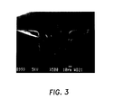
- the SEM is of a 100 thick film on a silicon wafer of a photoresist made by a procedure similar to that of Example 1 but without the copolymer.
- Soft bake 60°C/120 secs., 80°C/90 secs., and 90°C/90 secs. Exposure: Karl Suss, 22.8 J/cm 2 , contact. CD: 50 ⁇ .
- the SEM shows residual photoresist on the substrate at the bottom of the via and it shows the effects of outgassing and cracking of the photoresist.
- the substrate bearing it may be post-baked to increase the adhesion of the coating to the substrate and its resistance to plating solutions and the like.
Landscapes
- Physics & Mathematics (AREA)
- General Physics & Mathematics (AREA)
- Spectroscopy & Molecular Physics (AREA)
- Photosensitive Polymer And Photoresist Processing (AREA)
- Materials For Photolithography (AREA)
- Exposure Of Semiconductors, Excluding Electron Or Ion Beam Exposure (AREA)
- Exposure And Positioning Against Photoresist Photosensitive Materials (AREA)
Applications Claiming Priority (2)
| Application Number | Priority Date | Filing Date | Title |
|---|---|---|---|
| US93791392A | 1992-08-28 | 1992-08-28 | |
| US937913 | 1992-08-28 |
Publications (1)
| Publication Number | Publication Date |
|---|---|
| EP0588492A1 true EP0588492A1 (fr) | 1994-03-23 |
Family
ID=25470559
Family Applications (1)
| Application Number | Title | Priority Date | Filing Date |
|---|---|---|---|
| EP93306421A Withdrawn EP0588492A1 (fr) | 1992-08-28 | 1993-08-13 | Film épais et flexible de photorésistance positive ayant un haut facteur de forme |
Country Status (5)
| Country | Link |
|---|---|
| EP (1) | EP0588492A1 (fr) |
| JP (1) | JPH06202332A (fr) |
| KR (1) | KR960016316B1 (fr) |
| CA (1) | CA2097791A1 (fr) |
| IL (1) | IL105979A0 (fr) |
Cited By (12)
| Publication number | Priority date | Publication date | Assignee | Title |
|---|---|---|---|---|
| WO1996021175A1 (fr) * | 1994-12-30 | 1996-07-11 | Hoechst Celanese Corporation | Oligomeres de p-cresol a faible teneur en ions metal, et compositions photosensibles |
| US5624789A (en) * | 1992-07-10 | 1997-04-29 | Hoechst Celanese Corporation | Metal ion reduction in top anti-reflective coatings for photoresisis |
| US5656413A (en) * | 1995-09-28 | 1997-08-12 | Hoechst Celanese Corporation | Low metal ion containing 4,4'-[1-[4-[1-(4-Hydroxyphenyl)-1-methylethyl]phenyl]ethylidene]bisphe nol and photoresist compositions therefrom |
| US5665517A (en) * | 1996-01-11 | 1997-09-09 | Hoechst Celanese Corporation | Acidic ion exchange resin as a catalyst to synthesize a novolak resin and photoresist composition therefrom |
| US5750031A (en) * | 1995-09-26 | 1998-05-12 | Clariant Finance (Bvi) Limited | Process for producing surfactant having a low metal ion level and developer produced therefrom |
| US5830990A (en) * | 1992-07-10 | 1998-11-03 | Clariant Finance (Bvi) Limited | Low metals perfluorooctanoic acid and top anti-reflective coatings for photoresists |
| US5936071A (en) * | 1998-02-02 | 1999-08-10 | Clariant Finance (Bvi) Limited | Process for making a photoactive compound and photoresist therefrom |
| US5962183A (en) * | 1995-11-27 | 1999-10-05 | Clariant Finance (Bvi) Limited | Metal ion reduction in photoresist compositions by chelating ion exchange resin |
| US6911292B2 (en) | 2002-12-20 | 2005-06-28 | Shin-Etsu Chemical Co., Ltd. | Positive resist composition and patterning process |
| US8968982B2 (en) | 2011-01-19 | 2015-03-03 | Shin-Etsu Chemical Co., Ltd. | Chemically amplified positive resist composition and patterning process |
| US8980525B2 (en) | 2011-07-25 | 2015-03-17 | Shin-Etsu Chemical Co., Ltd. | Chemically amplified positive resist composition and patterning process |
| US9519217B2 (en) | 2014-06-09 | 2016-12-13 | Shin-Etsu Chemical Co., Ltd. | Chemically amplified positive resist composition and patterning process |
Families Citing this family (3)
| Publication number | Priority date | Publication date | Assignee | Title |
|---|---|---|---|---|
| KR100442859B1 (ko) * | 2001-04-04 | 2004-08-02 | 삼성전자주식회사 | 실리콘을 함유하는 알킬 비닐 에테르의 중합체로이루어지는 감광성 폴리머 및 이를 포함하는 레지스트조성물 |
| KR100493015B1 (ko) * | 2001-08-25 | 2005-06-07 | 삼성전자주식회사 | 감광성 폴리머 및 이를 포함하는 포토레지스트 조성물 |
| TWI724029B (zh) * | 2016-09-28 | 2021-04-11 | 奇美實業股份有限公司 | 化學增幅型正型感光性樹脂組成物、附有鑄模的基板的製造方法以及電鍍成形體的製造方法 |
Citations (4)
| Publication number | Priority date | Publication date | Assignee | Title |
|---|---|---|---|---|
| GB1243963A (en) * | 1967-08-15 | 1971-08-25 | Howson Algraphy Ltd | Improvements in or relating to light sensitive lithographic plates |
| US4448875A (en) * | 1983-03-31 | 1984-05-15 | Gaf Corporation | Electron beam sensitive mixture resist |
| US4728597A (en) * | 1987-02-17 | 1988-03-01 | Hoechst Celanese Corporation | Desensitizing solution for lithographic printing plates |
| DE3736996A1 (de) * | 1987-10-31 | 1989-05-11 | Basf Ag | Verfahren zur herstellung von copolymerisaten aus ethylenisch ungesaettigten dicarbonsaeureanhydriden und alkylvinylethern |
Family Cites Families (6)
| Publication number | Priority date | Publication date | Assignee | Title |
|---|---|---|---|---|
| JPS517402B2 (fr) * | 1973-04-23 | 1976-03-08 | ||
| JPS60111246A (ja) * | 1983-11-21 | 1985-06-17 | Fuji Photo Film Co Ltd | 感光性平版印刷版の現像液 |
| US4550069A (en) * | 1984-06-11 | 1985-10-29 | American Hoechst Corporation | Positive photoresist compositions with o-quinone diazide, novolak, and propylene glycol alkyl ether acetate |
| JPS63128335A (ja) * | 1986-11-19 | 1988-05-31 | Toshiba Corp | 感光性組成物及びパタ−ン形成方法 |
| CA2023423A1 (fr) * | 1989-09-05 | 1991-03-06 | Christopher E. Osuch | Agents transparents de modification de la vitesse de dissolution pour les resines photosensibles |
| CA2033403A1 (fr) * | 1990-01-26 | 1991-07-27 | Michael J. Mcfarland | Photoresist renfermant des di- et triesters aliphatiques de di- et triacides aromatiques et d'alcools |
-
1993
- 1993-06-04 CA CA002097791A patent/CA2097791A1/fr not_active Abandoned
- 1993-06-10 IL IL105979A patent/IL105979A0/xx unknown
- 1993-08-13 EP EP93306421A patent/EP0588492A1/fr not_active Withdrawn
- 1993-08-27 JP JP5235607A patent/JPH06202332A/ja active Pending
- 1993-08-28 KR KR1019930016899A patent/KR960016316B1/ko not_active Expired - Lifetime
Patent Citations (4)
| Publication number | Priority date | Publication date | Assignee | Title |
|---|---|---|---|---|
| GB1243963A (en) * | 1967-08-15 | 1971-08-25 | Howson Algraphy Ltd | Improvements in or relating to light sensitive lithographic plates |
| US4448875A (en) * | 1983-03-31 | 1984-05-15 | Gaf Corporation | Electron beam sensitive mixture resist |
| US4728597A (en) * | 1987-02-17 | 1988-03-01 | Hoechst Celanese Corporation | Desensitizing solution for lithographic printing plates |
| DE3736996A1 (de) * | 1987-10-31 | 1989-05-11 | Basf Ag | Verfahren zur herstellung von copolymerisaten aus ethylenisch ungesaettigten dicarbonsaeureanhydriden und alkylvinylethern |
Cited By (15)
| Publication number | Priority date | Publication date | Assignee | Title |
|---|---|---|---|---|
| US5624789A (en) * | 1992-07-10 | 1997-04-29 | Hoechst Celanese Corporation | Metal ion reduction in top anti-reflective coatings for photoresisis |
| US5830990A (en) * | 1992-07-10 | 1998-11-03 | Clariant Finance (Bvi) Limited | Low metals perfluorooctanoic acid and top anti-reflective coatings for photoresists |
| US5858627A (en) * | 1994-12-30 | 1999-01-12 | Clariant Finance (Bvi) Limited | Image formation utilizing photosensitive compositions containing low metal content p-cresol oligomers |
| WO1996021175A1 (fr) * | 1994-12-30 | 1996-07-11 | Hoechst Celanese Corporation | Oligomeres de p-cresol a faible teneur en ions metal, et compositions photosensibles |
| US5837417A (en) * | 1994-12-30 | 1998-11-17 | Clariant Finance (Bvi) Limited | Quinone diazide compositions containing low metals p-cresol oligomers and process of producing the composition |
| US5750031A (en) * | 1995-09-26 | 1998-05-12 | Clariant Finance (Bvi) Limited | Process for producing surfactant having a low metal ion level and developer produced therefrom |
| US5656413A (en) * | 1995-09-28 | 1997-08-12 | Hoechst Celanese Corporation | Low metal ion containing 4,4'-[1-[4-[1-(4-Hydroxyphenyl)-1-methylethyl]phenyl]ethylidene]bisphe nol and photoresist compositions therefrom |
| US5962183A (en) * | 1995-11-27 | 1999-10-05 | Clariant Finance (Bvi) Limited | Metal ion reduction in photoresist compositions by chelating ion exchange resin |
| US5665517A (en) * | 1996-01-11 | 1997-09-09 | Hoechst Celanese Corporation | Acidic ion exchange resin as a catalyst to synthesize a novolak resin and photoresist composition therefrom |
| US5936071A (en) * | 1998-02-02 | 1999-08-10 | Clariant Finance (Bvi) Limited | Process for making a photoactive compound and photoresist therefrom |
| US6048665A (en) * | 1998-02-02 | 2000-04-11 | Clariant Finance (Bvi) Limited | Process for making a photoactive compound and photoresist therefrom |
| US6911292B2 (en) | 2002-12-20 | 2005-06-28 | Shin-Etsu Chemical Co., Ltd. | Positive resist composition and patterning process |
| US8968982B2 (en) | 2011-01-19 | 2015-03-03 | Shin-Etsu Chemical Co., Ltd. | Chemically amplified positive resist composition and patterning process |
| US8980525B2 (en) | 2011-07-25 | 2015-03-17 | Shin-Etsu Chemical Co., Ltd. | Chemically amplified positive resist composition and patterning process |
| US9519217B2 (en) | 2014-06-09 | 2016-12-13 | Shin-Etsu Chemical Co., Ltd. | Chemically amplified positive resist composition and patterning process |
Also Published As
| Publication number | Publication date |
|---|---|
| KR940004381A (ko) | 1994-03-15 |
| KR960016316B1 (ko) | 1996-12-09 |
| JPH06202332A (ja) | 1994-07-22 |
| CA2097791A1 (fr) | 1994-03-01 |
| IL105979A0 (en) | 1993-10-20 |
Similar Documents
| Publication | Publication Date | Title |
|---|---|---|
| EP0588492A1 (fr) | Film épais et flexible de photorésistance positive ayant un haut facteur de forme | |
| US4339521A (en) | Heat resistant positive resists containing polyoxazoles | |
| US4173470A (en) | Novolak photoresist composition and preparation thereof | |
| EP0568476B1 (fr) | Matériau de réserve positif contenant du silicone, et son procédé d'utilisation pour la technologie d'empaquetage en couches minces | |
| KR930010774B1 (ko) | 방사선감수성 조성물, 이를 사용하여 제조한 기록물질, 및 내열성 기록 양각 상의 제조방법 | |
| US4526856A (en) | Low striation positive diazoketone resist composition with cyclic ketone(s) and aliphatic alcohol as solvents | |
| US4650741A (en) | Positive photosensitive composition of cocondensed β-naphthol and m-cresol with aldehyde in admixture with sulfonyl triester of a 1,2-naphthoquinone-1-diazide | |
| JP5320631B2 (ja) | 厚膜形成用のフォトレジスト組成物 | |
| US4873176A (en) | Reticulation resistant photoresist coating | |
| KR20010023776A (ko) | 저면 반사 방지막용 조성물 및 이에 사용하기 위한 신규중합체 염료 | |
| US20040023147A1 (en) | Positive photosensitive resin composition, process for its preparation, and semiconductor devices | |
| JPH09120163A (ja) | 反射防止コーティング | |
| EP0851305A1 (fr) | Procédé de rinçage et de décapage pour la lithographie | |
| US10976659B2 (en) | Photoresists comprising novolak resin blends | |
| CN1072813C (zh) | 正性光致抗蚀剂的显影方法和所用的组合物 | |
| EP3392708B1 (fr) | Stratifié de film à résistance positive et procédé de formation de motifs | |
| US5302490A (en) | Radiation sensitive compositions comprising blends of an aliphatic novolak resin and an aromatic novolak resin | |
| US5276126A (en) | Selected novolak resin planarization layer for lithographic applications | |
| US5858547A (en) | Novolac polymer planarization films for microelectronic structures | |
| JP4062087B2 (ja) | 感光性誘電体形成用組成物、転写フィルム、誘電体および電子部品 | |
| JPS62232989A (ja) | 基板上の回路線の形成方法 | |
| JP3549882B2 (ja) | ノボラック樹脂混合物 | |
| JP3078175B2 (ja) | 感光性樹脂組成物 | |
| US5853947A (en) | Quinonediazide positive photoresist utilizing mixed solvent consisting essentially of 3-methyl-3-methoxy butanol and propylene glycol alkyl ether acetate | |
| EP0345305A1 (fr) | Agent de photoreserve pour film sec a image reversible |
Legal Events
| Date | Code | Title | Description |
|---|---|---|---|
| PUAI | Public reference made under article 153(3) epc to a published international application that has entered the european phase |
Free format text: ORIGINAL CODE: 0009012 |
|
| AK | Designated contracting states |
Kind code of ref document: A1 Designated state(s): AT BE DE FR GB IT NL |
|
| 17P | Request for examination filed |
Effective date: 19940413 |
|
| STAA | Information on the status of an ep patent application or granted ep patent |
Free format text: STATUS: THE APPLICATION HAS BEEN WITHDRAWN |
|
| 18W | Application withdrawn |
Withdrawal date: 19950320 |