EP0589763A1 - Verfahren zum Verzögern eines Signals und zugehörige Verzögerungsschaltung - Google Patents
Verfahren zum Verzögern eines Signals und zugehörige Verzögerungsschaltung Download PDFInfo
- Publication number
- EP0589763A1 EP0589763A1 EP93402282A EP93402282A EP0589763A1 EP 0589763 A1 EP0589763 A1 EP 0589763A1 EP 93402282 A EP93402282 A EP 93402282A EP 93402282 A EP93402282 A EP 93402282A EP 0589763 A1 EP0589763 A1 EP 0589763A1
- Authority
- EP
- European Patent Office
- Prior art keywords
- circuit
- signal
- delay
- capacitive
- output
- Prior art date
- Legal status (The legal status is an assumption and is not a legal conclusion. Google has not performed a legal analysis and makes no representation as to the accuracy of the status listed.)
- Granted
Links
Images


Classifications
-
- H—ELECTRICITY
- H03—ELECTRONIC CIRCUITRY
- H03K—PULSE TECHNIQUE
- H03K5/00—Manipulating of pulses not covered by one of the other main groups of this subclass
- H03K5/13—Arrangements having a single output and transforming input signals into pulses delivered at desired time intervals
- H03K5/133—Arrangements having a single output and transforming input signals into pulses delivered at desired time intervals using a chain of active delay devices
-
- H—ELECTRICITY
- H03—ELECTRONIC CIRCUITRY
- H03K—PULSE TECHNIQUE
- H03K5/00—Manipulating of pulses not covered by one of the other main groups of this subclass
- H03K5/13—Arrangements having a single output and transforming input signals into pulses delivered at desired time intervals
- H03K5/131—Digitally controlled
-
- H—ELECTRICITY
- H03—ELECTRONIC CIRCUITRY
- H03K—PULSE TECHNIQUE
- H03K5/00—Manipulating of pulses not covered by one of the other main groups of this subclass
- H03K2005/00013—Delay, i.e. output pulse is delayed after input pulse and pulse length of output pulse is dependent on pulse length of input pulse
- H03K2005/00019—Variable delay
- H03K2005/00026—Variable delay controlled by an analog electrical signal, e.g. obtained after conversion by a D/A converter
- H03K2005/00032—DC control of switching transistors
- H03K2005/00039—DC control of switching transistors having four transistors serially
-
- H—ELECTRICITY
- H03—ELECTRONIC CIRCUITRY
- H03K—PULSE TECHNIQUE
- H03K5/00—Manipulating of pulses not covered by one of the other main groups of this subclass
- H03K2005/00013—Delay, i.e. output pulse is delayed after input pulse and pulse length of output pulse is dependent on pulse length of input pulse
- H03K2005/00019—Variable delay
- H03K2005/00058—Variable delay controlled by a digital setting
- H03K2005/00071—Variable delay controlled by a digital setting by adding capacitance as a load
-
- H—ELECTRICITY
- H03—ELECTRONIC CIRCUITRY
- H03K—PULSE TECHNIQUE
- H03K5/00—Manipulating of pulses not covered by one of the other main groups of this subclass
- H03K2005/00013—Delay, i.e. output pulse is delayed after input pulse and pulse length of output pulse is dependent on pulse length of input pulse
- H03K2005/0015—Layout of the delay element
- H03K2005/00195—Layout of the delay element using FET's
Definitions
- the invention relates to the development of a variable and controllable delay for temporally delaying a signal.
- variable delay circuits are used in many devices such as voltage controlled oscillators, phase control loops, delay lines or oversampling systems. Given this great utility, variable delay circuits have been the subject of numerous studies and have resulted in different production techniques that the person skilled in the art usually groups into three main families.
- the first family concerns delay circuits produced using differential amplifiers where the variation of the propagation time between the input and the output is obtained by acting on the common mode current.
- Such an embodiment is for example described in the article by Giebel et al., Digitally Controlled Oscillator, IEEE Journal of Solid-state Circuits, Vol. 24, No. 6, June 1989.
- Another family of delay circuits includes those known as current starving, which are based on conventional inverting structures, for example CMOS technology inverters whose propagation time varies according to the maximum supply current which is imposed on them by an appropriate control system.
- CMOS technology inverters whose propagation time varies according to the maximum supply current which is imposed on them by an appropriate control system.
- the third family groups the delay circuits with variable load which exploit the variation of the propagation time of a logic circuit, such as an inverter, according to the value of its output load.
- a logic circuit such as an inverter
- the output load consists of a field effect transistor connected in series with a capacity.
- the field effect transistor is controlled on its gate by a control signal and can be considered as a voltage-controlled resistor whose variation in value modifies the impedance of the output load and consequently the charge and discharge times. of capacity, which affects the value of the delay.
- the invention aims to provide a solution to these problems.
- the invention also aims to obtain a linearity of evolution of the delay as a function of the control signal.
- Another object of the invention is to directly control the variation of the delay from a digital signal.
- Another object of the invention is to propose a delay circuit, the very simple implementation of which does not require analog techniques.
- the subject of the invention is therefore a method for temporally delaying a signal of a variable and controllable delay in which a capacitive load of a load circuit is connected at the output of a logic circuit capable of receiving said signal at input and at outputting a delayed signal, and in which the impedance of the load circuit is modified to vary said delay; according to a general characteristic of the invention, the impedance of the load circuit is modified by modifying the intrinsic capacitive value of the capacitive load.
- Such a method thus makes it possible to advantageously control the modification of the values of the capacitive load from a digital word. It is thus possible to confer on the capacitive load discrete values taken from a determined set of values. According to a preferred embodiment, the capacitive load is successively given discrete values according to a substantially linear evolution.
- the subject of the invention is also a variable and controllable delay circuit, comprising a signal input, a control input for a control signal, a signal output for delivering a signal delayed in time relative to the input signal, and delay means comprising a logic circuit connected between the signal input and output, as well as a load circuit comprising a capacitive load connected at the output of the logic circuit, the load circuit impedance being modifiable under the action the control signal to vary said delay; according to a general characteristic of the invention, the capacitive load is variable under the action of the control signal to take different capacitive values.
- the capacitive load advantageously comprises at least one capacity controllable under the action of the control signal to assume a passive state in which it has no effect on the value of the delay, and an active state in which it influences the value of the delay.
- the capacitor comprises a field effect transistor with an insulated gate whose drain and source are connected to the output of the logic circuit and whose gate is connected to the control input; the capacitor is then in its active or passive state as a function of the value of the gate voltage relative to the threshold voltage of the transistor.
- the control signal advantageously comprises a digital word; also, the delay means comprise means capable of receiving the control signal and of delivering a control voltage to the gate of the transistor, capable of taking two different values as a function of the value of the digital word, these two values being located on either side of the threshold voltage.
- the capacitive load may include a plurality of capacitors connected at the output of the logic circuit, controllable individually or by group under the action of the control signal.
- the plurality of controllable capacitors connected in parallel to the output of the logic circuit have respective capacitive values forming a geometric sequence of reason 2, the control signal then comprising a plurality of successive digital words capable of successively activating at least one of the capacities in a predetermined order giving the capacitive load capacitive values forming an arithmetic sequence.
- each digital word of the control signal then activates at least one group of capacities in a predetermined order to obtain the pitch of said arithmetic sequence equal to the elementary capacity.
- the logic circuit is preferably an inverter comprising two complementary insulated gate field effect transistors, the P channel field effect transistor advantageously has a channel width greater than that of the N channel transistor of this inverter.
- the charging circuit may include a plurality of analog delay means and connected in series.
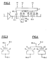
- the reference 1 designates a signal input of the delay circuit while the reference 2 relates to a signal output capable of delivering an output signal delayed in time relative to the input signal.
- This input signal SE is advantageously composed of alternating rising and falling edges.
- delay means here comprising a logic inverter 4 whose input is connected to the signal input and whose output 9 is connected to the signal output 2.
- This inverter 4 is here conventionally produced from two complementary insulated gate field effect transistors 5 and 8, whose respective drains D are connected to the output of the inverter and whose respective gates G are connected to the input of this inverter .
- the field effect transistors with insulated gates 5 and 8 have a resistive component, the resistive values of which have been schematically represented by two resistors 6 and 7 respectively connected between the drains of the transistors and the output of the inverter.
- a capacitive load 10 composed here of a plurality of capacitors in parallel 10-1 ... 10-n.
- This capacitive load 10 is connected to a control input 3, capable of receiving a control signal, by means of logic means 11 of which we will return in more detail to the structure and the function below.
- the capacitance 12 connected between the output 9 of the inverter and the ground represents the stray capacitance Cp of the circuit.
- the capacitive load 10, the stray capacitance 12 and the resistors 6 and 7 of the insulated gate field effect transistors 5 and 8 form a charging circuit for these delay means.
- the capacitive load 10 will successively charge and discharge through resistors 6 and 7.
- the inverter 4 will change state, that is to say say deliver a falling edge in the presence of a rising edge at the entry and vice versa, generally at the end of the time necessary for the charge capacitive to reach half of its charge.
- this charging and discharging time depends on the time constant RC of the charging circuit, where R denotes the resistive value and C the capacitive value of this charging circuit.
- this time constant is modified by directly modifying the intrinsic capacitive value of the capacitive load 10. This principle is therefore completely different from that known previously which consists in acting on the value of the resistance by modulating its value by a analog control signal (voltage or current).
- the control signal used here, and arriving at control input 3, is a digital word making it possible to activate or deactivate at least one of the capacities 10-1 ... 10-n of the capacitive load 10, according to the value of the bits of this digital word.
- a capacity will be considered to be activated and will then be in a so-called "active" state when, under the action of the control signal, it is likely to be charged and discharged to influence the value of the delay.
- such a capacity will be considered as deactivated, and will be in a passive state, when, under the action of the control signal, it will have no influence on the value of the delay.
- the capacitive load 10 is made up of several groups (here three) of capacities all having substantially the same basic intrinsic capacitive value C.
- the respective numbers of capacities of these different groups form a geometric sequence of reason 2.
- the first group 10- 1 has only one capacity while the second group 10-2 has two and the third group 10-3 has four. Therefore, one obtains, at the output of the inverter, a plurality of controllable capacitors having respective capacitive values forming a geometric sequence of reason 2 and first term.
- the capacitive value of the first group is equal to C, while that of the second group is equal to 2C and that of the third group is equal to 4C.
- the control signal will then advantageously be composed of several digital words each composed of a plurality of bits in a number equal to the plurality of groups (here three), all these digital words being capable of successively activating at least one of these groups in a predetermined order conferring on the capacitive load 10 capacitive values forming an arithmetic sequence of pitch equal to the value C of the elementary capacitance.
- each digital word of the control signal comprises three bits b1, b2, b3, and if the bits of each of these digital words are given, values such that the first group 10- are successively activated 1, then the second group, then the first and the second groups together, then the third group, then the third and the first groups together, and so on, we will obtain, for the capacitive load 10, values successively equal to C , 2C, 3C, 4C, 5C ....
- Each capacitor may consist of a field effect transistor with an insulated gate, for example with an N channel, as illustrated in FIG. 3.
- the gate G of this transistor is connected to terminal 100-1 which is itself connected. at the output of the means 11 while the source S and the drain D of such a transistor are connected together to the terminal 101-1 connected to the output 9 of the inverter.
- the capacity is in its active or passive state depending on the value of the gate voltage relative to the threshold voltage of the transistor. Indeed, if the gate voltage is at a voltage lower than the threshold voltage, the channel zone located under this gate is not depleted and the field effect transistor then has a capacitance connected between the gate and the substrate , which is therefore without influence vis-à-vis the inverter 4. On the other hand, if the gate is brought to a voltage higher than the threshold voltage, the channel zone is depleted and the transistor has a capacitance connected between the grid and the drain (and the source) which makes it active vis-à-vis the inverter 4.
- a capacitor of equivalent capacitive value controlled by a transistor, for example a field effect.
- the capacity would be connected between the drain of the transistor and the output 9 of the inverter and would be electrically incorporated in the load circuit depending on the gate voltage of the transistor then acting as a simple switch.
- transistors connected in parallel can be used, as illustrated in FIG. 4 for group 10-2.
- the two gates G1 and G2 of two transistors are connected together to terminal 100-2 while the sources S1 and S2 and the drains D1 and D2 of these two transistors are connected together to terminal 101-2.
- the means 11 are capable of receiving the control signal and of delivering a control voltage to the gate of the transistor, capable of taking two different values depending on the value of the digital word, these two values being located on either side. of the threshold voltage of the transistors.
- Use will be made, for example, of the means 11, of logic means such as logic gates delivering a gate control voltage, zero or equal to 5 Volts for example, as a function of the value of the input binary word.
- High-impedance direct digital control (that is to say without going through an analog control other than that consisting solely of the supply of two analog values corresponding directly to the two values of a bit) according to the invention, has made it possible to obtain, as illustrated in FIG. 5, a linearity of the variation of the propagation time Tp of the inverter as a function of the value of the control word, of the order of 1%.
- the values 0 to 7 correspond to the eight decimal values of the eight successive digital words of the control signal, each composed of the bits b3, b2, b1, the corresponding binary values of these words ranging from 000 to 111.
- the logic circuit used here is an inverter produced in CMOS technology although it is possible to use other logic circuits, for example based on NAND gates, provided that these other logic circuits are arranged so as not to cause excessive distortion. between the appearance of the input and output fronts, which could be misinterpreted as a delay.
- an inverter with two complementary insulated gate transistors it is preferable to provide transistors having selected dimensional characteristics so that these N and P channel transistors deliver the same maximum current under the same conditions .
- the value of this current depends on the mobility of the carriers and the dimensioning of the channel (length between drain and source, and width).
- a channel width for the P-channel transistor greater than that of the channel of the N-channel transistor.
- double channel width This avoids obtaining an output signal "narrowed" compared to the input signal, that is to say having a different spacing between the falling edges and the rising edges. Such a signal would be obtained with two complementary transistors with identical dimensional characteristics due to the higher resistive value of the P-channel transistor 5.
- FIG. 6 illustrates an embodiment of the invention, making it possible in particular to produce delay lines with multiple outputs, in which the delay circuit comprises a plurality of similar delay means 4-a, 10-a, 11-a; 4-b, 10-b, 11-b, connected in series between input 1 and output 2.
- the delay circuit comprises a plurality of similar delay means 4-a, 10-a, 11-a; 4-b, 10-b, 11-b, connected in series between input 1 and output 2.
- auxiliary inverters 14-a and 14-b connected at the output of each inverter 4-a and 4-b in order to decouple an elementary module from the next one and thus be able to take intermediate output signals from terminals 15-a and 15-b without influencing the value of the delay determined by the value of capacitive loads 10-a and 10-b.
Landscapes
- Physics & Mathematics (AREA)
- Nonlinear Science (AREA)
- Pulse Circuits (AREA)
- Networks Using Active Elements (AREA)
Applications Claiming Priority (2)
| Application Number | Priority Date | Filing Date | Title |
|---|---|---|---|
| FR9211267 | 1992-09-22 | ||
| FR9211267A FR2696061B1 (fr) | 1992-09-22 | 1992-09-22 | Procédé pour retarder temporellement un signal et circuit à retard correspondant. |
Publications (2)
| Publication Number | Publication Date |
|---|---|
| EP0589763A1 true EP0589763A1 (de) | 1994-03-30 |
| EP0589763B1 EP0589763B1 (de) | 1997-03-19 |
Family
ID=9433745
Family Applications (1)
| Application Number | Title | Priority Date | Filing Date |
|---|---|---|---|
| EP93402282A Expired - Lifetime EP0589763B1 (de) | 1992-09-22 | 1993-09-20 | Verzögerungsschaltung |
Country Status (5)
| Country | Link |
|---|---|
| US (1) | US5416436A (de) |
| EP (1) | EP0589763B1 (de) |
| JP (1) | JPH06204791A (de) |
| DE (1) | DE69308978T2 (de) |
| FR (1) | FR2696061B1 (de) |
Cited By (4)
| Publication number | Priority date | Publication date | Assignee | Title |
|---|---|---|---|---|
| EP0884846A1 (de) * | 1997-06-12 | 1998-12-16 | Hewlett-Packard Company | Verzögerungsschaltung mit Kalibrierung |
| EP0858161A3 (de) * | 1997-02-06 | 1999-11-17 | Nec Corporation | Verzögerungsschaltung mit Pulsformung |
| EP0895355A3 (de) * | 1997-07-29 | 2000-07-12 | Fujitsu Limited | Digital gesteuerte Verzögerungsschaltung |
| US6414531B2 (en) | 2000-02-09 | 2002-07-02 | Infineon Technologies Ag | Circuit configuration for adjusting signal delay times |
Families Citing this family (45)
| Publication number | Priority date | Publication date | Assignee | Title |
|---|---|---|---|---|
| DE19501707C1 (de) * | 1995-01-20 | 1996-06-05 | Texas Instruments Deutschland | Elektrisches Bauelement und Verfahren zum Abgleichen der inneren Laufzeit eines solchen elektrischen Bauelements |
| US5644262A (en) * | 1995-02-24 | 1997-07-01 | Intel Corporation | Digitally controlled capacitive load |
| JP3862306B2 (ja) * | 1995-06-23 | 2006-12-27 | 三菱電機株式会社 | 半導体装置 |
| US5714907A (en) * | 1996-07-29 | 1998-02-03 | Intel Corporation | Apparatus for providing digitally-adjustable floating MOS capacitance |
| JPH1049561A (ja) * | 1996-08-07 | 1998-02-20 | Mitsubishi Electric Corp | 信号遅延計算方法 |
| US5964884A (en) * | 1996-09-30 | 1999-10-12 | Advanced Micro Devices, Inc. | Self-timed pulse control circuit |
| US6115318A (en) * | 1996-12-03 | 2000-09-05 | Micron Technology, Inc. | Clock vernier adjustment |
| CA2224767A1 (en) * | 1996-12-31 | 1998-06-30 | Huang Chaogang | Variable cmos vernier delay |
| US5940608A (en) * | 1997-02-11 | 1999-08-17 | Micron Technology, Inc. | Method and apparatus for generating an internal clock signal that is synchronized to an external clock signal |
| US5920518A (en) * | 1997-02-11 | 1999-07-06 | Micron Technology, Inc. | Synchronous clock generator including delay-locked loop |
| US6912680B1 (en) | 1997-02-11 | 2005-06-28 | Micron Technology, Inc. | Memory system with dynamic timing correction |
| US5946244A (en) | 1997-03-05 | 1999-08-31 | Micron Technology, Inc. | Delay-locked loop with binary-coupled capacitor |
| US6173432B1 (en) * | 1997-06-20 | 2001-01-09 | Micron Technology, Inc. | Method and apparatus for generating a sequence of clock signals |
| US5953284A (en) * | 1997-07-09 | 1999-09-14 | Micron Technology, Inc. | Method and apparatus for adaptively adjusting the timing of a clock signal used to latch digital signals, and memory device using same |
| US6201412B1 (en) * | 1997-07-30 | 2001-03-13 | Matsushita Electric Industrial Co., Ltd. | Semiconductor integrated circuit with driver stabilization using parasitic capacitance |
| US6011732A (en) * | 1997-08-20 | 2000-01-04 | Micron Technology, Inc. | Synchronous clock generator including a compound delay-locked loop |
| US5926047A (en) | 1997-08-29 | 1999-07-20 | Micron Technology, Inc. | Synchronous clock generator including a delay-locked loop signal loss detector |
| US6101197A (en) | 1997-09-18 | 2000-08-08 | Micron Technology, Inc. | Method and apparatus for adjusting the timing of signals over fine and coarse ranges |
| KR100271633B1 (ko) * | 1997-11-01 | 2000-11-15 | 김영환 | 지연회로 |
| US6269451B1 (en) | 1998-02-27 | 2001-07-31 | Micron Technology, Inc. | Method and apparatus for adjusting data timing by delaying clock signal |
| US6016282A (en) * | 1998-05-28 | 2000-01-18 | Micron Technology, Inc. | Clock vernier adjustment |
| US6338127B1 (en) | 1998-08-28 | 2002-01-08 | Micron Technology, Inc. | Method and apparatus for resynchronizing a plurality of clock signals used to latch respective digital signals, and memory device using same |
| US6349399B1 (en) | 1998-09-03 | 2002-02-19 | Micron Technology, Inc. | Method and apparatus for generating expect data from a captured bit pattern, and memory device using same |
| US6279090B1 (en) | 1998-09-03 | 2001-08-21 | Micron Technology, Inc. | Method and apparatus for resynchronizing a plurality of clock signals used in latching respective digital signals applied to a packetized memory device |
| US6029250A (en) * | 1998-09-09 | 2000-02-22 | Micron Technology, Inc. | Method and apparatus for adaptively adjusting the timing offset between a clock signal and digital signals transmitted coincident with that clock signal, and memory device and system using same |
| JP2000138866A (ja) * | 1998-10-30 | 2000-05-16 | Nec Corp | 電荷結合素子の信号処理装置 |
| US6430696B1 (en) | 1998-11-30 | 2002-08-06 | Micron Technology, Inc. | Method and apparatus for high speed data capture utilizing bit-to-bit timing correction, and memory device using same |
| US6374360B1 (en) | 1998-12-11 | 2002-04-16 | Micron Technology, Inc. | Method and apparatus for bit-to-bit timing correction of a high speed memory bus |
| US6470060B1 (en) | 1999-03-01 | 2002-10-22 | Micron Technology, Inc. | Method and apparatus for generating a phase dependent control signal |
| JP2001307480A (ja) * | 2000-04-24 | 2001-11-02 | Mitsubishi Electric Corp | 半導体集積回路装置 |
| JP2002076855A (ja) | 2000-08-29 | 2002-03-15 | Advantest Corp | 遅延回路、試験装置、コンデンサ |
| DE10164822B4 (de) * | 2000-08-29 | 2007-04-12 | Advantest Corp. | Prüfvorrichtung |
| US6801989B2 (en) | 2001-06-28 | 2004-10-05 | Micron Technology, Inc. | Method and system for adjusting the timing offset between a clock signal and respective digital signals transmitted along with that clock signal, and memory device and computer system using same |
| US6628154B2 (en) * | 2001-07-31 | 2003-09-30 | Cypress Semiconductor Corp. | Digitally controlled analog delay locked loop (DLL) |
| US20030048123A1 (en) * | 2001-08-29 | 2003-03-13 | Sun Microsystems, Inc. | Integrated circuit and method of adjusting capacitance of a node of an integrated circuit |
| US6614275B1 (en) * | 2002-04-04 | 2003-09-02 | Sun Microsystems, Inc. | Adjustable capacitances for DLL loop and power supply noise filters |
| KR100482370B1 (ko) * | 2002-09-27 | 2005-04-13 | 삼성전자주식회사 | 게이트 산화막의 두께가 다른 반도체장치 |
| US7168027B2 (en) | 2003-06-12 | 2007-01-23 | Micron Technology, Inc. | Dynamic synchronization of data capture on an optical or other high speed communications link |
| US7234070B2 (en) | 2003-10-27 | 2007-06-19 | Micron Technology, Inc. | System and method for using a learning sequence to establish communications on a high-speed nonsynchronous interface in the absence of clock forwarding |
| EP1566888B1 (de) * | 2004-02-18 | 2007-05-23 | STMicroelectronics S.r.l. | Taktimpulsgenerator |
| US7283005B2 (en) * | 2004-02-10 | 2007-10-16 | Stmicroelectronics S.R.L. | Clock-pulse generator circuit |
| TWI358902B (en) * | 2007-12-31 | 2012-02-21 | Ind Tech Res Inst | Signal delay circuit |
| US8837229B1 (en) * | 2013-03-15 | 2014-09-16 | Synopsys, Inc. | Circuit for generating negative bitline voltage |
| US9698760B1 (en) * | 2014-01-31 | 2017-07-04 | Marvell International Ltd. | Continuous-time analog delay device |
| US9705484B2 (en) * | 2015-06-25 | 2017-07-11 | Mediatek Inc. | Delay cell in a standard cell library |
Citations (4)
| Publication number | Priority date | Publication date | Assignee | Title |
|---|---|---|---|---|
| EP0059802A1 (de) * | 1981-03-06 | 1982-09-15 | Deutsche ITT Industries GmbH | Integrierte Isolierschicht-Feldeffekttransistor-Verzögerungsschaltung für Digitalsignale und deren Verwendung in Farbfernsehempfängern |
| EP0423963A2 (de) * | 1989-10-16 | 1991-04-24 | Advanced Micro Devices, Inc. | Zeitverzögerungsschaltungen mit Temperaturkompensation |
| EP0439203A2 (de) * | 1986-06-16 | 1991-07-31 | Tektronix Inc. | Schaltung mit veränderlicher Verzögerung |
| EP0474534A1 (de) * | 1990-08-23 | 1992-03-11 | Bull S.A. | Schaltung mit einstellbarer Zeitkonstante und ihre Anwendung für einstellbare Verzögerungsleitung |
Family Cites Families (5)
| Publication number | Priority date | Publication date | Assignee | Title |
|---|---|---|---|---|
| US4016511A (en) * | 1975-12-19 | 1977-04-05 | The United States Of America As Represented By The Secretary Of The Air Force | Programmable variable length high speed digital delay line |
| JPS6089774A (ja) * | 1983-08-01 | 1985-05-20 | フエアチアイルド カメラ アンド インストルメント コ−ポレ−シヨン | 最小メモリを使用した自動テスト方式における信号タイミング装置の制御 |
| JP3019340B2 (ja) * | 1989-12-05 | 2000-03-13 | セイコーエプソン株式会社 | 可変容量装置 |
| KR930006228B1 (ko) * | 1990-07-20 | 1993-07-09 | 삼성전자 주식회사 | 신호지연회로 |
| EP0539831B1 (de) * | 1991-11-01 | 1998-06-03 | Hewlett-Packard Company | Programmierbares Kapazitätsverzögerungselement in Pseudo-NMOS-Technik |
-
1992
- 1992-09-22 FR FR9211267A patent/FR2696061B1/fr not_active Expired - Fee Related
-
1993
- 1993-09-20 DE DE69308978T patent/DE69308978T2/de not_active Expired - Fee Related
- 1993-09-20 EP EP93402282A patent/EP0589763B1/de not_active Expired - Lifetime
- 1993-09-20 JP JP5256357A patent/JPH06204791A/ja active Pending
- 1993-09-21 US US08/124,772 patent/US5416436A/en not_active Expired - Fee Related
Patent Citations (4)
| Publication number | Priority date | Publication date | Assignee | Title |
|---|---|---|---|---|
| EP0059802A1 (de) * | 1981-03-06 | 1982-09-15 | Deutsche ITT Industries GmbH | Integrierte Isolierschicht-Feldeffekttransistor-Verzögerungsschaltung für Digitalsignale und deren Verwendung in Farbfernsehempfängern |
| EP0439203A2 (de) * | 1986-06-16 | 1991-07-31 | Tektronix Inc. | Schaltung mit veränderlicher Verzögerung |
| EP0423963A2 (de) * | 1989-10-16 | 1991-04-24 | Advanced Micro Devices, Inc. | Zeitverzögerungsschaltungen mit Temperaturkompensation |
| EP0474534A1 (de) * | 1990-08-23 | 1992-03-11 | Bull S.A. | Schaltung mit einstellbarer Zeitkonstante und ihre Anwendung für einstellbare Verzögerungsleitung |
Cited By (9)
| Publication number | Priority date | Publication date | Assignee | Title |
|---|---|---|---|---|
| EP0858161A3 (de) * | 1997-02-06 | 1999-11-17 | Nec Corporation | Verzögerungsschaltung mit Pulsformung |
| US6121813A (en) * | 1997-02-06 | 2000-09-19 | Nec Corporation | Delay circuit having a noise reducing function |
| EP0884846A1 (de) * | 1997-06-12 | 1998-12-16 | Hewlett-Packard Company | Verzögerungsschaltung mit Kalibrierung |
| EP0895355A3 (de) * | 1997-07-29 | 2000-07-12 | Fujitsu Limited | Digital gesteuerte Verzögerungsschaltung |
| US6181184B1 (en) | 1997-07-29 | 2001-01-30 | Fujitsu Limited | Variable delay circuit and semiconductor intergrated circuit device |
| US6304117B1 (en) | 1997-07-29 | 2001-10-16 | Fujitsu Limited | Variable delay circuit and semiconductor integrated circuit device |
| US6549047B2 (en) | 1997-07-29 | 2003-04-15 | Fujitsu Limited | Variable delay circuit and semiconductor integrated circuit device |
| EP1555755A3 (de) * | 1997-07-29 | 2005-08-17 | Fujitsu Limited | Digital gesteuerte Verzögerungsschaltung |
| US6414531B2 (en) | 2000-02-09 | 2002-07-02 | Infineon Technologies Ag | Circuit configuration for adjusting signal delay times |
Also Published As
| Publication number | Publication date |
|---|---|
| FR2696061B1 (fr) | 1994-12-02 |
| FR2696061A1 (fr) | 1994-03-25 |
| EP0589763B1 (de) | 1997-03-19 |
| US5416436A (en) | 1995-05-16 |
| JPH06204791A (ja) | 1994-07-22 |
| DE69308978T2 (de) | 1997-09-04 |
| DE69308978D1 (de) | 1997-04-24 |
Similar Documents
| Publication | Publication Date | Title |
|---|---|---|
| EP0589763B1 (de) | Verzögerungsschaltung | |
| EP0562904B1 (de) | Verfahren und Vorrichtung zur Regelung einer Verzögerung über mehrere Verzögerungsbereiche | |
| EP2137873B1 (de) | Vorrichtung zur rückgewinnung des taktsignales zur digitalen regelung der phase ohne externe regelung | |
| EP2769473B1 (de) | Digital-analog-umsetzer | |
| EP0181664A1 (de) | Synchronisierter Komparator | |
| EP1863179B1 (de) | Niveauverschiebungsschaltkreis | |
| EP0562905B1 (de) | Schaltung mit veränderlicher Verzögerung | |
| FR2604839A1 (fr) | Procede pour reduire les effets du bruit electrique dans un convertisseur analogique/numerique | |
| EP0474534B1 (de) | Schaltung mit einstellbarer Zeitkonstante und ihre Anwendung für einstellbare Verzögerungsleitung | |
| EP0901227B1 (de) | Schaltung mit variabler Verzögerung | |
| FR2695505A1 (fr) | Circuits de mémorisation, de sommation et de conversion de tension et convertisseurs analogique-numérique. | |
| EP1925079B1 (de) | Stromschalter mit durch eine niederspannung gespeisten differenztransistorpaaren | |
| EP3654534B1 (de) | Kapazitive logische zelle | |
| FR2522221A1 (fr) | Circuit pour ameliorer le rendement de convertisseurs numeriques / analogiques | |
| FR2582462A1 (fr) | Filtre a memoire finie symetrique a condensateurs commutes | |
| EP0092879B1 (de) | Bitsynchronisiereinrichtung für Modulator-Demodulator oder Empfänger von Datenübertragung | |
| FR2792474A1 (fr) | Circuit de sortie de signal numerique | |
| FR2626102A1 (fr) | Memoire a transfert de charges et procede de fabrication de cette memoire | |
| FR2763443A1 (fr) | Circuit de sortie | |
| EP0346988A2 (de) | Integrierte Halbleiterschaltung mit synchronisiertem Komparator | |
| FR2783944A1 (fr) | Circuit de distribution de signal et procede de connexion de ligne de signal | |
| EP0187584B1 (de) | Logisches Koinzidenztor und dieses verwendende logische sequentielle Schaltungen | |
| GB2606797A (en) | Filters | |
| EP0332499B1 (de) | Schneller Komparator mit in zwei Phasen arbeitender Ausgangsstufe | |
| EP0349028A2 (de) | Integrierte Halbleiterschaltung mit einem differentiellen Paar von FETs |
Legal Events
| Date | Code | Title | Description |
|---|---|---|---|
| PUAI | Public reference made under article 153(3) epc to a published international application that has entered the european phase |
Free format text: ORIGINAL CODE: 0009012 |
|
| AK | Designated contracting states |
Kind code of ref document: A1 Designated state(s): DE GB |
|
| 17P | Request for examination filed |
Effective date: 19940829 |
|
| 17Q | First examination report despatched |
Effective date: 19950505 |
|
| GRAG | Despatch of communication of intention to grant |
Free format text: ORIGINAL CODE: EPIDOS AGRA |
|
| GRAH | Despatch of communication of intention to grant a patent |
Free format text: ORIGINAL CODE: EPIDOS IGRA |
|
| GRAH | Despatch of communication of intention to grant a patent |
Free format text: ORIGINAL CODE: EPIDOS IGRA |
|
| GRAA | (expected) grant |
Free format text: ORIGINAL CODE: 0009210 |
|
| AK | Designated contracting states |
Kind code of ref document: B1 Designated state(s): DE GB |
|
| REF | Corresponds to: |
Ref document number: 69308978 Country of ref document: DE Date of ref document: 19970424 |
|
| GBT | Gb: translation of ep patent filed (gb section 77(6)(a)/1977) |
Effective date: 19970408 |
|
| PLBE | No opposition filed within time limit |
Free format text: ORIGINAL CODE: 0009261 |
|
| STAA | Information on the status of an ep patent application or granted ep patent |
Free format text: STATUS: NO OPPOSITION FILED WITHIN TIME LIMIT |
|
| 26N | No opposition filed | ||
| PGFP | Annual fee paid to national office [announced via postgrant information from national office to epo] |
Ref country code: DE Payment date: 20000830 Year of fee payment: 8 |
|
| PGFP | Annual fee paid to national office [announced via postgrant information from national office to epo] |
Ref country code: GB Payment date: 20000831 Year of fee payment: 8 |
|
| PG25 | Lapsed in a contracting state [announced via postgrant information from national office to epo] |
Ref country code: GB Free format text: LAPSE BECAUSE OF NON-PAYMENT OF DUE FEES Effective date: 20010920 |
|
| REG | Reference to a national code |
Ref country code: GB Ref legal event code: IF02 |
|
| PG25 | Lapsed in a contracting state [announced via postgrant information from national office to epo] |
Ref country code: DE Free format text: LAPSE BECAUSE OF NON-PAYMENT OF DUE FEES Effective date: 20020501 |
|
| GBPC | Gb: european patent ceased through non-payment of renewal fee |
Effective date: 20010920 |