EP0901227B1 - Schaltung mit variabler Verzögerung - Google Patents
Schaltung mit variabler Verzögerung Download PDFInfo
- Publication number
- EP0901227B1 EP0901227B1 EP98402152A EP98402152A EP0901227B1 EP 0901227 B1 EP0901227 B1 EP 0901227B1 EP 98402152 A EP98402152 A EP 98402152A EP 98402152 A EP98402152 A EP 98402152A EP 0901227 B1 EP0901227 B1 EP 0901227B1
- Authority
- EP
- European Patent Office
- Prior art keywords
- delay
- circuit
- signal
- signals
- module
- Prior art date
- Legal status (The legal status is an assumption and is not a legal conclusion. Google has not performed a legal analysis and makes no representation as to the accuracy of the status listed.)
- Expired - Lifetime
Links
- 230000007704 transition Effects 0.000 claims description 18
- 239000003990 capacitor Substances 0.000 claims description 17
- 239000000872 buffer Substances 0.000 claims description 13
- 238000007493 shaping process Methods 0.000 claims description 11
- 230000001934 delay Effects 0.000 claims description 8
- 230000003111 delayed effect Effects 0.000 claims description 8
- 238000007599 discharging Methods 0.000 claims description 6
- 230000009471 action Effects 0.000 claims description 3
- 238000005259 measurement Methods 0.000 claims description 3
- 230000006870 function Effects 0.000 description 23
- 238000010586 diagram Methods 0.000 description 11
- 230000015654 memory Effects 0.000 description 9
- 230000004044 response Effects 0.000 description 8
- 230000006872 improvement Effects 0.000 description 7
- 230000000694 effects Effects 0.000 description 6
- 230000010354 integration Effects 0.000 description 6
- 238000005516 engineering process Methods 0.000 description 5
- 235000021183 entrée Nutrition 0.000 description 5
- 230000008901 benefit Effects 0.000 description 3
- 238000009826 distribution Methods 0.000 description 3
- 238000012886 linear function Methods 0.000 description 3
- 238000013459 approach Methods 0.000 description 2
- 230000008859 change Effects 0.000 description 2
- 230000000295 complement effect Effects 0.000 description 2
- 239000006185 dispersion Substances 0.000 description 2
- 238000004519 manufacturing process Methods 0.000 description 2
- PXFBZOLANLWPMH-UHFFFAOYSA-N 16-Epiaffinine Natural products C1C(C2=CC=CC=C2N2)=C2C(=O)CC2C(=CC)CN(C)C1C2CO PXFBZOLANLWPMH-UHFFFAOYSA-N 0.000 description 1
- 238000004458 analytical method Methods 0.000 description 1
- 238000004364 calculation method Methods 0.000 description 1
- 230000003750 conditioning effect Effects 0.000 description 1
- 230000003247 decreasing effect Effects 0.000 description 1
- 230000001419 dependent effect Effects 0.000 description 1
- 238000005304 joining Methods 0.000 description 1
- 238000000034 method Methods 0.000 description 1
- 230000010363 phase shift Effects 0.000 description 1
- 230000008569 process Effects 0.000 description 1
- 230000000630 rising effect Effects 0.000 description 1
- 230000035945 sensitivity Effects 0.000 description 1
- 230000008054 signal transmission Effects 0.000 description 1
Images



Classifications
-
- H—ELECTRICITY
- H03—ELECTRONIC CIRCUITRY
- H03K—PULSE TECHNIQUE
- H03K5/00—Manipulating of pulses not covered by one of the other main groups of this subclass
- H03K5/13—Arrangements having a single output and transforming input signals into pulses delivered at desired time intervals
- H03K5/133—Arrangements having a single output and transforming input signals into pulses delivered at desired time intervals using a chain of active delay devices
Definitions
- integration into the circuit combination is produced by an integrator or a time constant circuit always presenting a saturation effect defining the extreme levels of combination signal.
- a transition time is defined as the time interval during which the signal combination varies according to a linear function or quasi-linear when one of the coefficients of weighting associated with the intermediate signals is no.
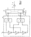
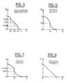
- the curves presented in FIGS. 2 to 9 make it possible to explain the operation of the circuit of FIG. 1. They explain the reasons which prevented the introduction of a simple circuit D1 with fixed delay equal to a time T 'greater than T which would have directly enlarged the delay range. They expose on the one hand the nature of the combination signals f K and of the output signals s K according to the comparison between the fixed delay time T between the signals m0 and m1 and a transition time tm.
- the transition time tm is the duration presented by the combination circuit for passing the signal Fk from its minimum value to its saturation value when K is 0 or 1.
- the figures show the variations of the delay t K in function of the coefficient K for different values of the transition time tm, the fixed delay T being assumed to be fixed.
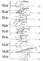
- the threshold value S1 corresponds to the average level between the minimum levels and maximum of signal m0. It is the same for the signal m1. In case the threshold value is set at medium level, these signals m0 and m1 could have a shape different from that shown.
- the delay T is defined as the time interval between instants when the signal m0 and the signal m1 reach the threshold value.
- the timing diagram in FIG. 2c represents the output signal from the shaping circuit F in each of the three cases represented in the timing diagram in FIG. 2b.
- the signals S1 and S0 have an edge respectively at times t1 and t0.
- the output signal s K will have a edge delayed by a value T K with respect to the signal S1, the value T K being between 0 and T, that is to say t1 + T with respect to m0.
- Figures 10 and 11 relate to an embodiment circuit diagram and in CMOS technology combination C.
- Each DC discharge circuit also includes a variable resistance R0 for U0, R1 for U1 and a switch N0 for U0 and N1 for U1.
- Each switch controls connection by resistance associated with it between line L and potential power supply Vdd for the load circuit and Vss for the discharge circuit.
- the switches of U0 and U1 units are controlled respectively by the signals m0 and m1 and their complement m0 * and m1 *.
- This second range Pl2 ends with a point c which corresponds to the maximum delay between r1 and r2 with 100% of the current passing through the module U0.
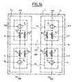
- the advantage of recommended connection mode in fact does not switch than a multiplexer (MUX0) taking into account the symmetrical character of the circuit of FIGS. 11 and 15. Then it is the turn of the MUX1 multiplexer to switch, the signal r1 giving way to signal r3.
- MUX0 multiplexer
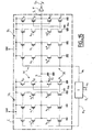
- transistors controlled by the coefficients K0, K1, etc ... have increasing grid widths binary (1, 2, 4, etc ).
- the transistor added in the additional branch has half grid width from the smallest of the previous grid widths.
- the branch added has a grid width half from that of other branches.
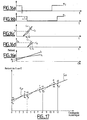
- Figures 16a and 16b are the timing diagrams of the signals m0 and m1 offset by a time T.
- the origin of time is defined when m0 switches to 0.
- the digital control can therefore order more effectively the values of the coefficients ki and the tilting of the multiplexers. Indeed, if this command results from a slave action, the fact that the servo has a negative slope (b b ', c c ') and in particular a vertex, in b or in c, of the gain curve, causes this servo to oscillate around the value associated with point b.
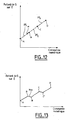
- Figure 17 also shows the comparison between the delay curves obtained: the curve Co1 representative of the delay time in the absence of branches permanently connected, and the Co2 curve characteristic of the delay time for the circuit including branches permanently connected.
- the Co2 curve that we are approaching a optimal linearity; the delay is so anyway always increased.
Landscapes
- Physics & Mathematics (AREA)
- Nonlinear Science (AREA)
- Pulse Circuits (AREA)
- Networks Using Active Elements (AREA)
Claims (7)
- Verzögerungsschaltung zum Bereitstellen eines Ausgangssignals (sK, welches in Bezug auf ein Eingangssignal (e0) eine Verzögerung () aufweist, wobei die Verzögerung () in Abhängigkeit von einer Verzögerungsanweisung (CN) steuerbar ist, wobei die Verzögerungsschaltung aufweist:wobei die Kombinationsschaltung aufweist,einen Primärkreis (D1), der das Eingangssignal (e0) empfängt und ein erstes und zweites Zwischensignal (m0, m1) bereitstellt, die untereinander eine feste Verzögerung (T) aufweisen,eine Kombinationsschaltung (C) mit zwei Eingängen (X, Y), wobei die Zwischensignale (m0, m1) an die Eingänge (X, Y) angelegt werden, wobei beim Ausgang ein Kombinationssignal (fK) bereitgestellt wird, das resultiert aus einer Überlagerung mit einer Gewichtsfunktion der Steuergröße (K) und einer Integrationswirkung der an deren Eingänge (X, Y) angelegten Signale,eine Aufbereitungsschaltung, die das Kombinationssignal empfängt, wobei das Ausgangssignal sK bereitgestellt wird, und einen Schwelleneffekt aufweist,wobei die Verzögerungsschaltung dadurch gekennzeichnet ist, dass jedes Modul (U0, U1) eine Entladungsschaltung (DC) und eine Ladungsschaltung (PC) aufweist, welche jeweils Schaltermittel (P0, N0, P1, N1) aufweisen, welche die Verbindung zwischen der gemeinsamen Leitung (L) und einem ersten beziehungsweise zweiten Versorgungspotential (Vss, Vdd) einesteils durch Vermittlung eines variablen Widerstands (R0, R0*, R1, R1*), anderenteils durch einen nicht-variablen Widerstand (R0f, R0f*, R1f, R1f*). steuern, der die permanente Teilnahme der zwei Module (U0 und U1) an der Ladung oder Entladung des Kondensators (C1) sicherstellt und dadurch dass die Schaltermittel (P0, N0, P1, N1) der Entladungsschaltung (DC) und der Ladungsschaltung (PC) von jedem Modul (U0, U1) durch die Zwischensignale (m0, m1) aktiviert werden.einen Steuereingang (CD), welcher eine für die Anweisung (CN) repräsentative Steuergröße (K) empfängt,eine gemeinsame Leitung (L) mit einem Kondensator (C1), der mit dieser gemeinsamen Leitung und einem Versorgungspotential verbunden ist,ein erstes und ein zweites Ladungs- und Entladungsmodul (U0, U1) der gemeinsamen Leitung (L), welche durch das erste beziehungsweise zweite Zwischensignal (m0, m1) gesteuert werden, wobei das Potential der gemeinsamen Leitung (L) die Erfassung des Kombinationssignals (fK) bildet,
- Verzögerungsschaltung nach Anspruch 1, dadurch gekennzeichnet, dass die feste Verzögerung (T) weniger als eine Übergangszeit (tm) beträgt, die das Kombinationssignal (fk) bereitstellt, wenn die Kombinationsschaltung (C) lediglich eines der beiden Signale (m0, m1) empfängt.
- Schaltung nach einem der Ansprüche 1 oder 2, dadurch gekennzeichnet, dass die Gewichtung darin besteht mit einem Gewichtskoeffizienten jedes der Signale beim Eintritt in die Kombinationsschaltung (C) zu gewichten, wobei die Werte der Gewichtskoeffizienten in Abhängigkeit von der Steuergröße (K) sind, wobei die Summe der zwei Gewichtskoeffizienten konstant ist, wobei der variable Widerstand (R0, R0*, R1, R1*) der Entladungs- und Ladungsschaltungen (DC, PC) von jedem Modul (U0, U1) derart gesteuert ist, einen zum Gewichtskoeffizienten von einem der Zwischensignale (m0, m1) invers proportionalen Wert anzunehmen.
- Verzögerungsschaltung nach einem der Ansprüche 1 bis 3, dadurch gekennzeichnet, dass die variablen Widerstände (R0, R0*, R1, R1*) von jedem Modul (U0, U1) mittels einer Anordnung von Elementarwiderständen verwirklicht sind, die selektiv in Abhängigkeit von dem Gewichtskoeffizienten des assoziierten Zwischensignals (m0, m1) an dem Modul (U0, U1) parallelgeschaltet werden können.
- Verzögerungsschaltung nach einem der Ansprüche 1 bis 4, dadurch gekennzeichnet, dass die variablen Widerstände (R0, R0*, R1, R1*), die nicht-variablen Widerstände (R0f, R0f*, R1f, R1f*) und die Schalter (P0, N0, P1, N1) durch die Wege Drain-Source von MOS-Transistoren gebildet sind, deren Gates in Abhängigkeit von Gewichtskoeffizienten durch die assoziierten Signale (m0, m1) oder durch konstante Potentiale gesteuert sind.
- Verzögerungssehaltung nach einem der Ansprüche 1 bis 5, dadurch gekennzeichnet, dass ein Ladungs- und Entladungsmodul drei Zweige aufweist, die durch ein Gewichtssignal (K) und einen Zweig unter dauernder Leitung gesteuert sind.
- Verzögerungsschaltung nach einem der Ansprüche 1 bis 6, dadurch gekennzeichnet, dass in der Verzögerungsschaltung die Primärschaltung (D1) mittels eines Satzes serieller Pufferspeicher (T1, T2, T3) verwirklicht ist, wobei für jeden das Signal bei dessen Ausgang um eine Verzögerung (T) verzögert wird, wobei man am Ausgang von ihnen mindestens ein erstes und zweites verzögertes Signal (r1, r2) erhält, wobei das Eingangssignal (e0) und die verzögerten Signale (r1, r2) an Eingänge eines ersten und einesizweiten Multiplexers (MUX0, MUX1) angelegt sind, welche das erste und zweite Zwischensignal (m0, m1) bereitstellen.
Applications Claiming Priority (2)
| Application Number | Priority Date | Filing Date | Title |
|---|---|---|---|
| FR9711022 | 1997-09-04 | ||
| FR9711022A FR2767982B1 (fr) | 1997-09-04 | 1997-09-04 | Circuit a retard variable |
Publications (2)
| Publication Number | Publication Date |
|---|---|
| EP0901227A1 EP0901227A1 (de) | 1999-03-10 |
| EP0901227B1 true EP0901227B1 (de) | 2004-01-21 |
Family
ID=9510769
Family Applications (1)
| Application Number | Title | Priority Date | Filing Date |
|---|---|---|---|
| EP98402152A Expired - Lifetime EP0901227B1 (de) | 1997-09-04 | 1998-08-31 | Schaltung mit variabler Verzögerung |
Country Status (5)
| Country | Link |
|---|---|
| US (1) | US6169436B1 (de) |
| EP (1) | EP0901227B1 (de) |
| JP (1) | JP3470946B2 (de) |
| DE (1) | DE69821175D1 (de) |
| FR (1) | FR2767982B1 (de) |
Families Citing this family (17)
| Publication number | Priority date | Publication date | Assignee | Title |
|---|---|---|---|---|
| EP1128292A1 (de) * | 1998-01-22 | 2001-08-29 | Bull S.A. | Verfahren zur Abschätzung der Eignung einer Vlsi-Schaltung zum Widerstehen von Übersprechraushen |
| US6970313B1 (en) | 1999-03-31 | 2005-11-29 | Matsushita Electric Industrial Co., Ltd. | Write compensation circuit and signal interpolation circuit of recording device |
| JP3297738B2 (ja) * | 2000-02-16 | 2002-07-02 | 東北大学長 | Cmos多数決回路 |
| US6684311B2 (en) * | 2001-06-22 | 2004-01-27 | Intel Corporation | Method and mechanism for common scheduling in a RDRAM system |
| JP3810316B2 (ja) * | 2001-12-26 | 2006-08-16 | 沖電気工業株式会社 | 周波数逓倍回路 |
| US7515656B2 (en) * | 2002-04-15 | 2009-04-07 | Fujitsu Limited | Clock recovery circuit and data receiving circuit |
| FR2844655A1 (fr) * | 2002-09-13 | 2004-03-19 | St Microelectronics Sa | Transformation d'un signal periodique en un signal de frequence ajustable |
| EP1505732B1 (de) * | 2003-07-31 | 2007-09-26 | STMicroelectronics Pvt. Ltd | Digitaler Taktmodulator |
| US7116147B2 (en) * | 2004-10-18 | 2006-10-03 | Freescale Semiconductor, Inc. | Circuit and method for interpolative delay |
| US7323918B1 (en) * | 2006-08-08 | 2008-01-29 | Micrel, Incorporated | Mutual-interpolating delay-locked loop for high-frequency multiphase clock generation |
| US7737750B2 (en) * | 2007-01-16 | 2010-06-15 | Infineon Technologies Ag | Method and device for determining trim solution |
| TWI364165B (en) * | 2008-07-21 | 2012-05-11 | Univ Nat Chiao Tung | Absolute delay generating device |
| EP3451035B1 (de) | 2010-02-03 | 2019-11-27 | Tyco Electronics Nederland B.V. | Gehäuseanordnung für einen verbinder, entlastungselement und verfahren |
| US9166574B2 (en) | 2010-12-17 | 2015-10-20 | Keysight Technologies, Inc. | Apparatus and method for providing timing adjustment of input signal |
| US9306551B2 (en) * | 2013-01-22 | 2016-04-05 | Mediatek Inc. | Interpolator and interpolation cells with non-uniform driving capabilities therein |
| US9106230B1 (en) * | 2013-03-14 | 2015-08-11 | Altera Corporation | Input-output circuitry for integrated circuits |
| CN105493405B (zh) * | 2013-08-19 | 2018-09-25 | 国立研究开发法人科学技术振兴机构 | 可重构的延迟电路及使用该延迟电路的延迟监测电路、偏差校正电路、偏差测定方法和偏差校正方法 |
Family Cites Families (4)
| Publication number | Priority date | Publication date | Assignee | Title |
|---|---|---|---|---|
| US4797586A (en) * | 1987-11-25 | 1989-01-10 | Tektronix, Inc. | Controllable delay circuit |
| FR2689339B1 (fr) * | 1992-03-24 | 1996-12-13 | Bull Sa | Procede et dispositif de reglage de retard a plusieurs gammes. |
| FR2690022B1 (fr) * | 1992-03-24 | 1997-07-11 | Bull Sa | Circuit a retard variable. |
| US5374860A (en) * | 1993-01-15 | 1994-12-20 | National Semiconductor Corporation | Multi-tap digital delay line |
-
1997
- 1997-09-04 FR FR9711022A patent/FR2767982B1/fr not_active Expired - Fee Related
-
1998
- 1998-08-31 DE DE69821175T patent/DE69821175D1/de not_active Expired - Lifetime
- 1998-08-31 EP EP98402152A patent/EP0901227B1/de not_active Expired - Lifetime
- 1998-09-03 US US09/146,602 patent/US6169436B1/en not_active Expired - Fee Related
- 1998-09-04 JP JP25120698A patent/JP3470946B2/ja not_active Expired - Fee Related
Also Published As
| Publication number | Publication date |
|---|---|
| DE69821175D1 (de) | 2004-02-26 |
| JPH11168364A (ja) | 1999-06-22 |
| FR2767982B1 (fr) | 2001-11-23 |
| JP3470946B2 (ja) | 2003-11-25 |
| US6169436B1 (en) | 2001-01-02 |
| FR2767982A1 (fr) | 1999-03-05 |
| EP0901227A1 (de) | 1999-03-10 |
Similar Documents
| Publication | Publication Date | Title |
|---|---|---|
| EP0901227B1 (de) | Schaltung mit variabler Verzögerung | |
| EP0562904B1 (de) | Verfahren und Vorrichtung zur Regelung einer Verzögerung über mehrere Verzögerungsbereiche | |
| EP0562905B1 (de) | Schaltung mit veränderlicher Verzögerung | |
| EP2769473B1 (de) | Digital-analog-umsetzer | |
| FR2635239A1 (fr) | Element a retard pour circuit numerique | |
| EP0014628B1 (de) | N-Pfad-Frequenzfolge-Filter | |
| EP0474534B1 (de) | Schaltung mit einstellbarer Zeitkonstante und ihre Anwendung für einstellbare Verzögerungsleitung | |
| EP0493238B1 (de) | Schutzschaltung gegen Kurzschlüsse für elektronische Schalter | |
| CH625373A5 (de) | ||
| EP3667915A1 (de) | Verzögerungsschaltkreis | |
| EP2131494A1 (de) | Schaltkreis mit geschalteten Kapazitäten mit geringem Energieverbrauch | |
| FR2911449A1 (fr) | Filtre echantillonne a reponse impulsionnelle finie | |
| EP0932094A1 (de) | Vorrichtung zur Erzeugung rauscharmer Stromstösse | |
| EP2327160B1 (de) | Analogzähler und ein einen solchen zähler enthaltenden bildgeber | |
| FR2499788A1 (fr) | Circuit generateur d'impulsions utilisant une source de courant et ensemble de memorisation utilisant un tel circuit | |
| FR2461958A1 (fr) | Circuit de comparaison de phase | |
| EP3654534A1 (de) | Kapazitive logische zelle | |
| EP1845619A1 (de) | Pufferkreis, der Mittel zur Steuerung der Steilheit des Ausgangssignals umfasst | |
| EP0835550B1 (de) | Phasenkomparator ohne totbereich | |
| FR2649265A1 (fr) | Circuit amplificateur-separateur pour la conversion ttl-cmos | |
| EP3667914A1 (de) | Kalibrierung eines verzögerungsschaltkreises | |
| EP0092879A2 (de) | Bitsynchronisiereinrichtung für Modulator-Demodulator oder Empfänger von Datenübertragung | |
| EP0872960A1 (de) | Digitale Abgleichanordnung | |
| FR2575013A1 (fr) | Porte logique a coincidence, et circuits logiques sequentiels mettant en oeuvre cette porte a coincidence | |
| FR2767243A1 (fr) | Dispositif adaptateur symetrique de commutation d'un signal logique |
Legal Events
| Date | Code | Title | Description |
|---|---|---|---|
| PUAI | Public reference made under article 153(3) epc to a published international application that has entered the european phase |
Free format text: ORIGINAL CODE: 0009012 |
|
| AK | Designated contracting states |
Kind code of ref document: A1 Designated state(s): DE FR GB IT |
|
| AX | Request for extension of the european patent |
Free format text: AL;LT;LV;MK;RO;SI |
|
| 17P | Request for examination filed |
Effective date: 19990331 |
|
| AKX | Designation fees paid |
Free format text: DE FR GB IT |
|
| RAP1 | Party data changed (applicant data changed or rights of an application transferred) |
Owner name: STMICROELECTRONICS S.A. |
|
| GRAP | Despatch of communication of intention to grant a patent |
Free format text: ORIGINAL CODE: EPIDOSNIGR1 |
|
| GRAS | Grant fee paid |
Free format text: ORIGINAL CODE: EPIDOSNIGR3 |
|
| GRAA | (expected) grant |
Free format text: ORIGINAL CODE: 0009210 |
|
| AK | Designated contracting states |
Kind code of ref document: B1 Designated state(s): DE FR GB IT |
|
| PG25 | Lapsed in a contracting state [announced via postgrant information from national office to epo] |
Ref country code: IT Free format text: LAPSE BECAUSE OF FAILURE TO SUBMIT A TRANSLATION OF THE DESCRIPTION OR TO PAY THE FEE WITHIN THE PRE;WARNING: LAPSES OF ITALIAN PATENTS WITH EFFECTIVE DATE BEFORE 2007 MAY HAVE OCCURRED AT ANY TIME BEFORE 2007. THE CORRECT EFFECTIVE DATE MAY BE DIFFERENT FROM THE ONE RECORDED.SCRIBED TIME-LIMIT Effective date: 20040121 |
|
| REG | Reference to a national code |
Ref country code: GB Ref legal event code: FG4D Free format text: NOT ENGLISH |
|
| REF | Corresponds to: |
Ref document number: 69821175 Country of ref document: DE Date of ref document: 20040226 Kind code of ref document: P |
|
| GBT | Gb: translation of ep patent filed (gb section 77(6)(a)/1977) |
Effective date: 20040226 |
|
| PG25 | Lapsed in a contracting state [announced via postgrant information from national office to epo] |
Ref country code: DE Free format text: LAPSE BECAUSE OF FAILURE TO SUBMIT A TRANSLATION OF THE DESCRIPTION OR TO PAY THE FEE WITHIN THE PRESCRIBED TIME-LIMIT Effective date: 20040422 |
|
| PLBE | No opposition filed within time limit |
Free format text: ORIGINAL CODE: 0009261 |
|
| STAA | Information on the status of an ep patent application or granted ep patent |
Free format text: STATUS: NO OPPOSITION FILED WITHIN TIME LIMIT |
|
| 26N | No opposition filed |
Effective date: 20041022 |
|
| PGFP | Annual fee paid to national office [announced via postgrant information from national office to epo] |
Ref country code: FR Payment date: 20060808 Year of fee payment: 9 |
|
| PGFP | Annual fee paid to national office [announced via postgrant information from national office to epo] |
Ref country code: GB Payment date: 20060830 Year of fee payment: 9 |
|
| GBPC | Gb: european patent ceased through non-payment of renewal fee |
Effective date: 20070831 |
|
| REG | Reference to a national code |
Ref country code: FR Ref legal event code: ST Effective date: 20080430 |
|
| PG25 | Lapsed in a contracting state [announced via postgrant information from national office to epo] |
Ref country code: FR Free format text: LAPSE BECAUSE OF NON-PAYMENT OF DUE FEES Effective date: 20070831 |
|
| PG25 | Lapsed in a contracting state [announced via postgrant information from national office to epo] |
Ref country code: GB Free format text: LAPSE BECAUSE OF NON-PAYMENT OF DUE FEES Effective date: 20070831 |