EP0590220A1 - Circuit amplificateur de tension à haute fiabilité et faible dissipation - Google Patents
Circuit amplificateur de tension à haute fiabilité et faible dissipation Download PDFInfo
- Publication number
- EP0590220A1 EP0590220A1 EP92830530A EP92830530A EP0590220A1 EP 0590220 A1 EP0590220 A1 EP 0590220A1 EP 92830530 A EP92830530 A EP 92830530A EP 92830530 A EP92830530 A EP 92830530A EP 0590220 A1 EP0590220 A1 EP 0590220A1
- Authority
- EP
- European Patent Office
- Prior art keywords
- circuit
- fly
- power device
- input
- switching
- Prior art date
- Legal status (The legal status is an assumption and is not a legal conclusion. Google has not performed a legal analysis and makes no representation as to the accuracy of the status listed.)
- Granted
Links
Images

Classifications
-
- H—ELECTRICITY
- H02—GENERATION; CONVERSION OR DISTRIBUTION OF ELECTRIC POWER
- H02M—APPARATUS FOR CONVERSION BETWEEN AC AND AC, BETWEEN AC AND DC, OR BETWEEN DC AND DC, AND FOR USE WITH MAINS OR SIMILAR POWER SUPPLY SYSTEMS; CONVERSION OF DC OR AC INPUT POWER INTO SURGE OUTPUT POWER; CONTROL OR REGULATION THEREOF
- H02M3/00—Conversion of DC power input into DC power output
- H02M3/02—Conversion of DC power input into DC power output without intermediate conversion into AC
- H02M3/04—Conversion of DC power input into DC power output without intermediate conversion into AC by static converters
- H02M3/10—Conversion of DC power input into DC power output without intermediate conversion into AC by static converters using discharge tubes with control electrode or semiconductor devices with control electrode
- H02M3/145—Conversion of DC power input into DC power output without intermediate conversion into AC by static converters using discharge tubes with control electrode or semiconductor devices with control electrode using devices of a triode or transistor type requiring continuous application of a control signal
- H02M3/155—Conversion of DC power input into DC power output without intermediate conversion into AC by static converters using discharge tubes with control electrode or semiconductor devices with control electrode using devices of a triode or transistor type requiring continuous application of a control signal using semiconductor devices only
- H02M3/156—Conversion of DC power input into DC power output without intermediate conversion into AC by static converters using discharge tubes with control electrode or semiconductor devices with control electrode using devices of a triode or transistor type requiring continuous application of a control signal using semiconductor devices only with automatic control of output voltage or current, e.g. switching regulators
Definitions
- the present invention relates to a switching power supply circuit destined to function in a discontinuous mode; i.e. with a momentary nullification of the current through a "fly-back" inductance between successive impulses. More particularly the invention relates to an improved system for controlling the switching-on of a power device whereby besides reducing power consumption, a higher reliability and immunity to noise of the circuit are also achieved.
- a switching power supply commonly based on a so-called boost-type circuit utilizing a fly-back inductance, provides an output DC voltage having a value greater than the value of the input voltage, i.e. of the value of the rectified line voltage. If for any accidental cause, the output voltage becomes lower than the rectified line voltage, the circuit operates under anomalous conditions which: under certain circumstances, may lead to failure.
- Such an inductance is commonly referred to as a fly- back inductance because alternately during each switching cycle it firstly absorbs energy from the "low" voltage side (i.e. through the terminal connected to the rectified line voltage) during a conducting phase of the power device (transistor), and thereafter, following the switching-off of the power transistor (i.e. conduction taking place through an output diode), it gives back (flies-back) the energy stored in the inductance at the output voltage, releasing it to an utilizer circuit connected thereto.
- a fly- back inductance because alternately during each switching cycle it firstly absorbs energy from the "low" voltage side (i.e. through the terminal connected to the rectified line voltage) during a conducting phase of the power device (transistor), and thereafter, following the switching-off of the power transistor (i.e. conduction taking place through an output diode), it gives back (flies-back) the energy stored in the inductance at the output voltage, releasing it to an utilizer circuit connected thereto.
- the current across the inductance is made to vary between two limit values of the same sign, different from each other by not more than about ten or more percentage points, as referred to the amplitude of the rectified waveform.
- This first technique is preferred for high-power systems, because, for the same power, the introduction electromagnetic interferences in the line may be contained by employing a relatively inexpensive filter circuit, though requiring a more sophisticated switching circuit.
- the current flowing through the inductance has a high frequency saw-tooth waveform having a relatively small amplitude (ripple).
- an alternative technique said of discontinuous mode, is widely employed in power supplies of relatively low power; typically up to one or two hundreds watts.
- the current that circulates in the fly- back inductance is made to vary, during each switching cycle, between zero and a maximum value which follows the envelope of the rectified waveform.
- a switch-on signal is commonly obtained by detecting, on a dedicated secondary winding Ls magnetically coupled to the fly-back inductance L, a condition of null voltage across the secondary winding Ls.
- a switch-off signal for the power device is normally obtained through a comparison between a reference signal, that may be purposely generated within a PWM driving circuit and the current which flows through the power device Pw, which is commonly red on a sensing resistance Rsense; connected in series with the power transistor Pw.
- the power transistor When the sensed current reaches a reference threshold the power transistor is turned-off.
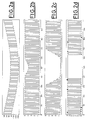
- the rectified line voltage V in is substantially present on the node C while on the other terminal of the fly-back inductance L, i.e. on the D node, a square wave voltage is present that takes a substantially null value when the power transistor Pw is conducting and a V out value (i.e. the output voltage of the power supply) when the power transistor Pw is not conducting. Therefore, the voltage signal that is induced on the secondary winding Ls, i.e. the voltage present on the node A, has a waveform that is enveloped at the top and at the bottom by a sinusoid, as depicted in Fig. 2a.
- This voltage signal through the resistance R1, is fed to a clipping circuit composed of the transistor Q1 ,the bias current generator Ib, the pair of series connected diodes D1 and D2, and the Zener diode DZ1, as shown in Fig. 1.
- This circuit limits the amplitude of a signal that is a replica of the voltage induced on the secondary winding Ls, on the node B (i.e. output node of the clipping circuit), as represented in Fig. 2b.
- This limited (clipped) voltage signal is compared with a reference voltage, schematically indicated in Fig. 1 by a battery symbol, by the comparator COMP, capable of producing a switch-on signal for the power device Pw that is sent to an input of a PWM driving circuit.
- Vmin (V out - V in )/K , where K is the L/Ls transformer ratio.
- any noise or spurious spike that may superimpose to the waveform of V in may simulate spurious transitions of the represented signal.
- the positive or negative transitions as referred to the sense of the magnetic coupling of the secondary winding Ls with the fly-back (primary) winding L, that identify the instant when the voltage across the fly-back inductance drops from V out - V in to zero and that are utilized for generating a switch-on signal for the power transitor Pw.
- the current flowing in the fly-back inductance has a substantially triangular wave shape (in practice the shape of a nonisosceles triangle of variable aspect) the amplitude of which varies from zero to a maximum that is enveloped by the rectified half-wave of the line voltage (V in ).
- V in line voltage
- the control system of the invention prevents the transfer of a switch-on signal, as generated by elaborating the signal present across a secondary winding magnetically, coupled with the winding (primary) of the fly-back inductance, to a Pulse-With-Modulation (PWM) driving circuit, as long as a current flowing through the fly-back inductance is detected. Notably, this does not alter the sensing of the optimum instant for switching-off the power transistor by the PWM driving circuit.
- PWM Pulse-With-Modulation
- the circuit object of the present invention is particularly suited when the line voltage has a relatively high form factor or presents noise spikes, as well as in all those instances when the output voltage, because of a certain variation of the load of the power supply, is subjected to a so-called "under-shoot” phenomenon, as related to the design regulated output voltage.
- the latter being a phenomenon that is practically inevitable when the switching power supply is provided with means for implementing also a function of control on the power factor (PFC).
- a circuit for controlling the switching-on of a power transistor Pw of a boost- type power supply circuit comprises a null detector circuit ⁇ -DETECT, a comparator COMP and a logic AND gate.
- the circuit for controlling the instant of switching-on of the power transistor and the relative PWM driving circuit may be integrated on a single chip, as indicatively shown in Fig. 3 by the dash line perimeter and by the relevant pins for connecting the integrated circuit to the external components of the power supply circuit.
- the current IL that flows through the fly-back inductance L of the circuit flows also through the sensing resistance Rsense during all phases of operation of the power supply circuit. Therefore, across the sensing resistor Rsense a voltage Vs proportional to the value of the current IL, is available.
- a voltage Vs proportional to the value of the current IL.
- Vref an ENABLE signal is produced that enables or disable the logic AND gate that transfers a signal commanding the switching-on of the power transistor Pw to an input terminal of the pulse width modulation driving circuit PWM.
- the reference voltage Vref sets the condition for enabling the switching-on of the power device Pw when IL drops below a certain safety value.
- a switch-on signal is actually produced by the null detector circuit ⁇ -DETECT whenever the voltage on the node A becomes null; however this signal is not transferred to the PWM driving circuit until the AND gate is enabled.
- the utilizer circuit powered by the power supply of the invention will have as reference common potential a virtual ground potential that is equivalent to the voltage present on the sensing resistance Rsense. In general, this peculiarity of the circuit of the invention will not create any problem.
Landscapes
- Engineering & Computer Science (AREA)
- Power Engineering (AREA)
- Dc-Dc Converters (AREA)
- Rectifiers (AREA)
- Direct Current Feeding And Distribution (AREA)
Priority Applications (4)
| Application Number | Priority Date | Filing Date | Title |
|---|---|---|---|
| DE69211345T DE69211345T2 (de) | 1992-09-28 | 1992-09-28 | Hochzwerlässige verlustarme Boosterschaltung |
| EP92830530A EP0590220B1 (fr) | 1992-09-28 | 1992-09-28 | Circuit amplificateur de tension à haute fiabilité et faible dissipation |
| US08/128,791 US5508602A (en) | 1992-09-28 | 1993-09-28 | Voltage boosting circuit with load current sensing |
| JP5265748A JPH06217531A (ja) | 1992-09-28 | 1993-09-28 | 高信頼及び低浪費型ブースト回路 |
Applications Claiming Priority (1)
| Application Number | Priority Date | Filing Date | Title |
|---|---|---|---|
| EP92830530A EP0590220B1 (fr) | 1992-09-28 | 1992-09-28 | Circuit amplificateur de tension à haute fiabilité et faible dissipation |
Publications (2)
| Publication Number | Publication Date |
|---|---|
| EP0590220A1 true EP0590220A1 (fr) | 1994-04-06 |
| EP0590220B1 EP0590220B1 (fr) | 1996-06-05 |
Family
ID=8212180
Family Applications (1)
| Application Number | Title | Priority Date | Filing Date |
|---|---|---|---|
| EP92830530A Expired - Lifetime EP0590220B1 (fr) | 1992-09-28 | 1992-09-28 | Circuit amplificateur de tension à haute fiabilité et faible dissipation |
Country Status (4)
| Country | Link |
|---|---|
| US (1) | US5508602A (fr) |
| EP (1) | EP0590220B1 (fr) |
| JP (1) | JPH06217531A (fr) |
| DE (1) | DE69211345T2 (fr) |
Cited By (1)
| Publication number | Priority date | Publication date | Assignee | Title |
|---|---|---|---|---|
| WO2001082459A1 (fr) * | 2000-04-21 | 2001-11-01 | Koninklijke Philips Electronics N.V. | Convertisseur ca-cc |
Families Citing this family (28)
| Publication number | Priority date | Publication date | Assignee | Title |
|---|---|---|---|---|
| EP0688076B1 (fr) * | 1994-06-13 | 1997-11-12 | BULL HN INFORMATION SYSTEMS ITALIA S.p.A. | Alimentation avec correction du facteur de puissance et protection contre la défaillance de la correction du facteur de puissance |
| US5694310A (en) * | 1995-08-14 | 1997-12-02 | International Business Machines Corporation | Three phase input boost converter |
| JPH09140145A (ja) * | 1995-11-15 | 1997-05-27 | Samsung Electron Co Ltd | 力率補償回路を備えた昇圧型コンバータ |
| KR0152252B1 (ko) * | 1995-11-16 | 1999-05-01 | 김광호 | 5핀을 갖는 능동역률보정집적회로 |
| US5929614A (en) * | 1997-06-13 | 1999-07-27 | Northrop Grumman Corporation | High efficiency DC step-up voltage converter |
| US6037754A (en) * | 1997-06-20 | 2000-03-14 | Raymond G. Harper | SMPS with input voltage sensing via boost inductor current sensing |
| US5982639A (en) * | 1997-11-04 | 1999-11-09 | Power Integrations, Inc. | Two switch off-line switching converter |
| US6876181B1 (en) * | 1998-02-27 | 2005-04-05 | Power Integrations, Inc. | Off-line converter with digital control |
| US6226190B1 (en) * | 1998-02-27 | 2001-05-01 | Power Integrations, Inc. | Off-line converter with digital control |
| US6107851A (en) | 1998-05-18 | 2000-08-22 | Power Integrations, Inc. | Offline converter with integrated softstart and frequency jitter |
| US5982644A (en) * | 1998-12-16 | 1999-11-09 | Hughes Electronics Corporation | Voltage boost circuit for a high voltage converter |
| US6296065B1 (en) | 1998-12-30 | 2001-10-02 | Black & Decker Inc. | Dual-mode non-isolated corded system for transportable cordless power tools |
| US6525514B1 (en) * | 2000-08-08 | 2003-02-25 | Power Integrations, Inc. | Method and apparatus for reducing audio noise in a switching regulator |
| US20040183769A1 (en) * | 2000-09-08 | 2004-09-23 | Earl Schreyer | Graphics digitizer |
| AU2002213225A1 (en) * | 2000-10-13 | 2002-04-22 | Primarion, Inc. | System and method for detection of zero current condition |
| US7812576B2 (en) | 2004-09-24 | 2010-10-12 | Marvell World Trade Ltd. | Power factor control systems and methods |
| US20060245816A1 (en) * | 2005-04-29 | 2006-11-02 | Kimberly-Clark Worldwide, Inc. | Fabric cleaning article |
| US7233504B2 (en) | 2005-08-26 | 2007-06-19 | Power Integration, Inc. | Method and apparatus for digital control of a switching regulator |
| US20080106917A1 (en) * | 2006-11-02 | 2008-05-08 | James Holt | Variable edge modulation in a switching regulator |
| US8018694B1 (en) | 2007-02-16 | 2011-09-13 | Fairchild Semiconductor Corporation | Over-current protection for a power converter |
| US7719243B1 (en) | 2007-11-21 | 2010-05-18 | Fairchild Semiconductor Corporation | Soft-start system and method for power converter |
| US7872883B1 (en) | 2008-01-29 | 2011-01-18 | Fairchild Semiconductor Corporation | Synchronous buck power converter with free-running oscillator |
| US7723972B1 (en) | 2008-03-19 | 2010-05-25 | Fairchild Semiconductor Corporation | Reducing soft start delay and providing soft recovery in power system controllers |
| TWI470915B (zh) * | 2008-03-21 | 2015-01-21 | Marvell World Trade Ltd | 升壓轉換器及功率因數控制器 |
| TW201032448A (en) | 2009-02-23 | 2010-09-01 | Delta Electronics Inc | Power conversion circuit capable of distributing input current |
| CN101820217B (zh) | 2009-02-26 | 2013-02-20 | 台达电子工业股份有限公司 | 具有分散输入电流功能的电源转换电路 |
| KR102277667B1 (ko) * | 2014-07-22 | 2021-07-15 | 삼성전자 주식회사 | 전자장치, 전원공급장치 및 그 전원제어방법 |
| US10090757B2 (en) | 2016-08-19 | 2018-10-02 | Fairchild Semiconductor Corporation | Power factor correction circuit and method |
Citations (2)
| Publication number | Priority date | Publication date | Assignee | Title |
|---|---|---|---|---|
| GB2198561A (en) * | 1986-11-26 | 1988-06-15 | Toshiba Kk | Electric converting circuit with control through photocoupler |
| GB2213614A (en) * | 1988-01-11 | 1989-08-16 | Farnell Instr | Waveform control arrangement for a switched mode power supply |
Family Cites Families (1)
| Publication number | Priority date | Publication date | Assignee | Title |
|---|---|---|---|---|
| US4709322A (en) * | 1985-07-26 | 1987-11-24 | Fred Mirow | High efficiency transformerless AC/DC converter |
-
1992
- 1992-09-28 DE DE69211345T patent/DE69211345T2/de not_active Expired - Fee Related
- 1992-09-28 EP EP92830530A patent/EP0590220B1/fr not_active Expired - Lifetime
-
1993
- 1993-09-28 US US08/128,791 patent/US5508602A/en not_active Expired - Lifetime
- 1993-09-28 JP JP5265748A patent/JPH06217531A/ja active Pending
Patent Citations (2)
| Publication number | Priority date | Publication date | Assignee | Title |
|---|---|---|---|---|
| GB2198561A (en) * | 1986-11-26 | 1988-06-15 | Toshiba Kk | Electric converting circuit with control through photocoupler |
| GB2213614A (en) * | 1988-01-11 | 1989-08-16 | Farnell Instr | Waveform control arrangement for a switched mode power supply |
Cited By (1)
| Publication number | Priority date | Publication date | Assignee | Title |
|---|---|---|---|---|
| WO2001082459A1 (fr) * | 2000-04-21 | 2001-11-01 | Koninklijke Philips Electronics N.V. | Convertisseur ca-cc |
Also Published As
| Publication number | Publication date |
|---|---|
| DE69211345T2 (de) | 1996-12-19 |
| EP0590220B1 (fr) | 1996-06-05 |
| DE69211345D1 (de) | 1996-07-11 |
| US5508602A (en) | 1996-04-16 |
| JPH06217531A (ja) | 1994-08-05 |
Similar Documents
| Publication | Publication Date | Title |
|---|---|---|
| EP0590220B1 (fr) | Circuit amplificateur de tension à haute fiabilité et faible dissipation | |
| EP0688076B1 (fr) | Alimentation avec correction du facteur de puissance et protection contre la défaillance de la correction du facteur de puissance | |
| CA1248583A (fr) | Circuit commutateur de puissance | |
| US4888821A (en) | Synchronization circuit for a resonant flyback high voltage supply | |
| US5398182A (en) | Power supply | |
| US4623960A (en) | Bias power source energized by tertiary winding including hysteresis characteristic for disabling the power switch when a minimum base drive signal can no longer be maintained | |
| US5072353A (en) | Circuit configuration for a blocking oscillator converter switching power supply | |
| CA1104205A (fr) | Traduction non-disponible | |
| JPH07177745A (ja) | スイッチングレギュレータ | |
| US20090096384A1 (en) | Universal dimmer | |
| US4158881A (en) | DC to DC converter | |
| US7049793B2 (en) | Boost switching power supply | |
| EP1206829B1 (fr) | Circuit d'attaque extremement efficace pour commutateur a semi-conducteur | |
| EP0948241A2 (fr) | Procédé et appareil pour alimenter des diodes électroluminescentes | |
| US6208089B1 (en) | Discharge-lamp lighting circuit | |
| US4876497A (en) | Power factor corrector | |
| US5406469A (en) | Electronic switching power supply | |
| EP0385544B1 (fr) | Circuit d'alimentation à découpage | |
| EP0067174B1 (fr) | Circuit de suralimentation en energie electrique de retour | |
| EP0031986A1 (fr) | Dispositif de protection contre la surintensité | |
| KR900002394B1 (ko) | 방전등(放電燈)의 점등장치 | |
| JPS60194757A (ja) | スイツチング電源装置 | |
| JPS6377383A (ja) | 起動回路 | |
| KR100434148B1 (ko) | 입력 과전압 보호 기능이 있는 전력변환시스템의 정류회로 | |
| JPH0261232B2 (fr) |
Legal Events
| Date | Code | Title | Description |
|---|---|---|---|
| PUAI | Public reference made under article 153(3) epc to a published international application that has entered the european phase |
Free format text: ORIGINAL CODE: 0009012 |
|
| AK | Designated contracting states |
Kind code of ref document: A1 Designated state(s): DE FR GB IT |
|
| 17P | Request for examination filed |
Effective date: 19940922 |
|
| 17Q | First examination report despatched |
Effective date: 19950308 |
|
| GRAH | Despatch of communication of intention to grant a patent |
Free format text: ORIGINAL CODE: EPIDOS IGRA |
|
| GRAA | (expected) grant |
Free format text: ORIGINAL CODE: 0009210 |
|
| AK | Designated contracting states |
Kind code of ref document: B1 Designated state(s): DE FR GB IT |
|
| REF | Corresponds to: |
Ref document number: 69211345 Country of ref document: DE Date of ref document: 19960711 |
|
| ITF | It: translation for a ep patent filed | ||
| ET | Fr: translation filed | ||
| PLBE | No opposition filed within time limit |
Free format text: ORIGINAL CODE: 0009261 |
|
| 26N | No opposition filed | ||
| REG | Reference to a national code |
Ref country code: GB Ref legal event code: IF02 |
|
| PGFP | Annual fee paid to national office [announced via postgrant information from national office to epo] |
Ref country code: DE Payment date: 20021002 Year of fee payment: 11 |
|
| PG25 | Lapsed in a contracting state [announced via postgrant information from national office to epo] |
Ref country code: DE Free format text: LAPSE BECAUSE OF NON-PAYMENT OF DUE FEES Effective date: 20040401 |
|
| PGFP | Annual fee paid to national office [announced via postgrant information from national office to epo] |
Ref country code: FR Payment date: 20040908 Year of fee payment: 13 |
|
| PGFP | Annual fee paid to national office [announced via postgrant information from national office to epo] |
Ref country code: GB Payment date: 20040922 Year of fee payment: 13 |
|
| PG25 | Lapsed in a contracting state [announced via postgrant information from national office to epo] |
Ref country code: IT Free format text: LAPSE BECAUSE OF NON-PAYMENT OF DUE FEES Effective date: 20050928 Ref country code: GB Free format text: LAPSE BECAUSE OF NON-PAYMENT OF DUE FEES Effective date: 20050928 |
|
| GBPC | Gb: european patent ceased through non-payment of renewal fee |
Effective date: 20050928 |
|
| PG25 | Lapsed in a contracting state [announced via postgrant information from national office to epo] |
Ref country code: FR Free format text: LAPSE BECAUSE OF NON-PAYMENT OF DUE FEES Effective date: 20060531 |
|
| REG | Reference to a national code |
Ref country code: FR Ref legal event code: ST Effective date: 20060531 |