EP0591437B1 - Verteilte multiprozessor-initialisierung und selbstprüfungssystem - Google Patents
Verteilte multiprozessor-initialisierung und selbstprüfungssystem Download PDFInfo
- Publication number
- EP0591437B1 EP0591437B1 EP92915004A EP92915004A EP0591437B1 EP 0591437 B1 EP0591437 B1 EP 0591437B1 EP 92915004 A EP92915004 A EP 92915004A EP 92915004 A EP92915004 A EP 92915004A EP 0591437 B1 EP0591437 B1 EP 0591437B1
- Authority
- EP
- European Patent Office
- Prior art keywords
- boot
- slot
- processing unit
- central processing
- default
- Prior art date
- Legal status (The legal status is an assumption and is not a legal conclusion. Google has not performed a legal analysis and makes no representation as to the accuracy of the status listed.)
- Expired - Lifetime
Links
Images


Classifications
-
- G—PHYSICS
- G06—COMPUTING OR CALCULATING; COUNTING
- G06F—ELECTRIC DIGITAL DATA PROCESSING
- G06F15/00—Digital computers in general; Data processing equipment in general
- G06F15/16—Combinations of two or more digital computers each having at least an arithmetic unit, a program unit and a register, e.g. for a simultaneous processing of several programs
- G06F15/177—Initialisation or configuration control
-
- G—PHYSICS
- G06—COMPUTING OR CALCULATING; COUNTING
- G06F—ELECTRIC DIGITAL DATA PROCESSING
- G06F11/00—Error detection; Error correction; Monitoring
- G06F11/07—Responding to the occurrence of a fault, e.g. fault tolerance
- G06F11/0703—Error or fault processing not based on redundancy, i.e. by taking additional measures to deal with the error or fault not making use of redundancy in operation, in hardware, or in data representation
- G06F11/0706—Error or fault processing not based on redundancy, i.e. by taking additional measures to deal with the error or fault not making use of redundancy in operation, in hardware, or in data representation the processing taking place on a specific hardware platform or in a specific software environment
- G06F11/0721—Error or fault processing not based on redundancy, i.e. by taking additional measures to deal with the error or fault not making use of redundancy in operation, in hardware, or in data representation the processing taking place on a specific hardware platform or in a specific software environment within a central processing unit [CPU]
- G06F11/0724—Error or fault processing not based on redundancy, i.e. by taking additional measures to deal with the error or fault not making use of redundancy in operation, in hardware, or in data representation the processing taking place on a specific hardware platform or in a specific software environment within a central processing unit [CPU] in a multiprocessor or a multi-core unit
-
- G—PHYSICS
- G06—COMPUTING OR CALCULATING; COUNTING
- G06F—ELECTRIC DIGITAL DATA PROCESSING
- G06F11/00—Error detection; Error correction; Monitoring
- G06F11/07—Responding to the occurrence of a fault, e.g. fault tolerance
- G06F11/14—Error detection or correction of the data by redundancy in operations
- G06F11/1402—Saving, restoring, recovering or retrying
- G06F11/1415—Saving, restoring, recovering or retrying at system level
- G06F11/1417—Boot up procedures
-
- G—PHYSICS
- G06—COMPUTING OR CALCULATING; COUNTING
- G06F—ELECTRIC DIGITAL DATA PROCESSING
- G06F12/00—Accessing, addressing or allocating within memory systems or architectures
- G06F12/02—Addressing or allocation; Relocation
- G06F12/06—Addressing a physical block of locations, e.g. base addressing, module addressing, memory dedication
- G06F12/0638—Combination of memories, e.g. ROM and RAM such as to permit replacement or supplementing of words in one module by words in another module
-
- G—PHYSICS
- G06—COMPUTING OR CALCULATING; COUNTING
- G06F—ELECTRIC DIGITAL DATA PROCESSING
- G06F9/00—Arrangements for program control, e.g. control units
- G06F9/06—Arrangements for program control, e.g. control units using stored programs, i.e. using an internal store of processing equipment to receive or retain programs
- G06F9/44—Arrangements for executing specific programs
- G06F9/4401—Bootstrapping
- G06F9/4405—Initialisation of multiprocessor systems
-
- G—PHYSICS
- G06—COMPUTING OR CALCULATING; COUNTING
- G06F—ELECTRIC DIGITAL DATA PROCESSING
- G06F11/00—Error detection; Error correction; Monitoring
- G06F11/07—Responding to the occurrence of a fault, e.g. fault tolerance
- G06F11/0703—Error or fault processing not based on redundancy, i.e. by taking additional measures to deal with the error or fault not making use of redundancy in operation, in hardware, or in data representation
- G06F11/0751—Error or fault detection not based on redundancy
- G06F11/0754—Error or fault detection not based on redundancy by exceeding limits
- G06F11/0757—Error or fault detection not based on redundancy by exceeding limits by exceeding a time limit, i.e. time-out, e.g. watchdogs
-
- G—PHYSICS
- G06—COMPUTING OR CALCULATING; COUNTING
- G06F—ELECTRIC DIGITAL DATA PROCESSING
- G06F11/00—Error detection; Error correction; Monitoring
- G06F11/22—Detection or location of defective computer hardware by testing during standby operation or during idle time, e.g. start-up testing
- G06F11/2205—Detection or location of defective computer hardware by testing during standby operation or during idle time, e.g. start-up testing using arrangements specific to the hardware being tested
- G06F11/2236—Detection or location of defective computer hardware by testing during standby operation or during idle time, e.g. start-up testing using arrangements specific to the hardware being tested to test CPU or processors
-
- G—PHYSICS
- G06—COMPUTING OR CALCULATING; COUNTING
- G06F—ELECTRIC DIGITAL DATA PROCESSING
- G06F11/00—Error detection; Error correction; Monitoring
- G06F11/22—Detection or location of defective computer hardware by testing during standby operation or during idle time, e.g. start-up testing
- G06F11/2205—Detection or location of defective computer hardware by testing during standby operation or during idle time, e.g. start-up testing using arrangements specific to the hardware being tested
- G06F11/2236—Detection or location of defective computer hardware by testing during standby operation or during idle time, e.g. start-up testing using arrangements specific to the hardware being tested to test CPU or processors
- G06F11/2242—Detection or location of defective computer hardware by testing during standby operation or during idle time, e.g. start-up testing using arrangements specific to the hardware being tested to test CPU or processors in multi-processor systems, e.g. one processor becoming the primary tester
Definitions
- the present invention relates to management of initialization operations in multiprocessor computer systems. Specifically, the invention relates to a method and apparatus to automatically control the determination of which processor in the system will boot the system. If the boot processor fails, control automatically shifts to an alternate processor. Additionally, the present invention involves a system wherein each central processing unit includes a corresponding copy of its own boot code. The boot code is transferred to memory for execution by the corresponding processor to carry out initialization operations.
- the computers servicing these needs are single processor systems conforming to conventional architectures using a standard input/output I/O bus such as the Extended Industry Standard Architecture (EISA).
- EISA Extended Industry Standard Architecture
- New and more powerful systems constantly emerge.
- upgrading an old system generally requires investing in substantial hardware modifications or buying a new system.
- CUPID architecture designed by AST Research Inc.
- the microprocessor based central processing unit CPU
- the backplane bus is not permanently attached to the backplane bus, but is a removable circuit board running at its own speed, asynchronous with the backplane bus operations.
- a faster CPU can replace the existing CPU.
- Japanese Patent Abstract No., vol. 012, no. 319 for Application no. JP860230633 is directed to the automatic selection of an initialization processing master CPU in a multi-processor system.
- the initialization of the master CPU is based on a prescribed priority by using a flag register which shows the priority for setting a master CPU.
- IBM Technical Disclosure Bulletin, vol. 33, no. 4, paqes 375-376 describes another approach for selecting a start-up master processor in a multi-processor system. Each processor conducts a self-test. The processors are polled and whichever processor completes its self-test first will be selected as the start-up master processor.
- neither of these approaches initialize multiple processor systems in an adequate manner.
- a number of problems hamper the development of such a multiprocessor architecture, such as, determining which processor boots the system, and, if one processor fails to boot the system, enabling another alternate processor to take over boot operations. Moreover, if after one processor boots the system (by executing instructions out of a read-only-memory (ROM)), but another processor utilizes a different instruction set than the boot processor installed in the system, then this other processor will require access to a different boot ROM.
- ROM read-only-memory
- the present invention provides a system and a method for coordinating the initialization of multiprocessor systems according to claim 1 and claim 8 respectively.
- Advantageous embodiments are found in the subclaims.
- the architecture provides a method and apparatus to interface multiple processors to a backplane system bus such that upon start-up of the computer system, one first default boot CPU is designated to boot the system while at least a second CPU is held in reset. If the default boot CPU fails to boot, the default boot CPU is held in reset and the second CPU is released from reset so it may attempt to boot. This provides fault tolerance and high availability for the system.
- a multiprocessor system utilizes a multiprocessor backplane bus.
- the backplane bus has connector slots for connecting multiple central processing units, memory modules, and other input/output modules.
- the system includes a default boot central processing unit.
- the default boot central processing unit has a first bus interface.
- the first bus interface is coupled to the backplane bus in a first slot.
- the system also includes at least one alternate boot central processing unit which has a second bus interface.
- the second bus interface is coupled to the backplane bus in a second slot.
- a first slot select unit is coupled to the default boot central processing unit by a select signal line.
- the first slot select unit is configured to release the default boot central processing unit from a reset state upon system start-up and allow the default central processing unit to execute boot code.
- the first slot select unit is further configured to place the default boot central processing unit in a reset state if a first predetermined time-out period, selected by a first respective slot identification code, elapses before the default central processing unit successfully
- a second slot select circuit is coupled to the alternate boot central processing unit by the select signal line.
- the second slot select circuit is configured to hold the alternate processing unit in a reset state until either the default boot central processing unit successfully boots, or a second predetermined time-out period, selected by a second respective slot identification code, elapses. The elapse of the second predetermined time-out indicates that the default boot central processing unit failed to boot the system.
- the second slot select circuit is further configured to release the alternate boot central processing unit from the reset state after the default central processing unit successfully boots or the second predetermined time-out period elapses.
- the second predetermined time-out period is longer than the first pre-determined time-out period.
- the second predetermined time-out period is equal to the first pre-determined time-out period.
- the default boot central processing unit is an INTEL ® 80486 based compatible processor and supporting resources
- the alternate boot central processing unit comprises is an INTEL ® 80486 based compatible processor and supporting resources.
- the default boot central processing unit includes a non-volatile memory storing at least portions of the boot code.
- the boot code includes initialization and self-test code.
- the initialization and self-test code is configured to be executed out of a centrally accessible memory module.
- the system for coordinating the initialization of multiprocessor systems includes a timer select circuit configured to select-the first predetermined time-out period and the second predetermined time-out period.
- system for coordinating the initialization of multiprocessor systems includes a system boot ROM containing a portion of the boot code.
- the boot ROM is accessible by the default boot central processing unit and the alternate boot central processing unit.
- Yet another aspect of the present invention is a method of coordinating the initialization of a multiprocessor system comprising the step of releasing a default boot central processing unit from a reset state upon system start-up, while holding an alternate boot central processing unit in a the reset state.
- the method further comprises the step of waiting a predetermined first time-out period for the default boot central processing unit to execute a first boot code.
- the method further comprises the step of placing the default processing unit in the reset state if the default boot processing unit fails to boot within the first predetermined time-out period.
- the method also includes the step of releasing the alternate boot central processing unit from the reset state if the default boot processor successfully boots within the first pre-determined time-out period.
- the method further comprises the step of releasing the alternate boot central processing unit from the reset state after a second predetermined time-out period elapses after the default boot central processing unit fails to boot.
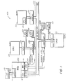
- Figure 1 is a block diagram of an exemplary multiprocessor interconnection system with a backplane system bus according to the present invention.
- FIG 2 is a more detailed block diagram of the input/output services module (IOSM) shown in Figure 1.
- IOSM input/output services module
- Figure 3 is a block diagram of a configuration of a multiprocessor interconnection system with three central processing units and illustrates the slot select interconnections between the IOSM and the slot select circuits of the present invention.
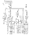
- Figure 4 is a schematic diagram of the slot select logic of the present invention.
- FIG. 1 is a block diagram of a multiprocessor interconnection system 100.
- the system 100 of the present embodiment comprises, in general, a backplane system bus 102 with a 64-bit multiple processor data bus 104, an input/output (I/O) bus 103, which advantageously comprises a 32-bit Extended Industry Standard Architecture (EISA) bus in the present embodiment, an input/output services module (IOSM) 108 with a corresponding bus controller 112, a conventional I/O controller(s) 118, a first central processing unit (CPU1) 120 with a corresponding cache 124 and bus controller 126, a memory module 130 with a corresponding bus interface 131, and a second central processing unit (CPU2) 132 with a corresponding cache 136 and bus controller 138.
- IOSM input/output services module
- the I/O controller(s) 118 comprise(s) conventional EISA or ISA compatible controller(s) in the present embodiment.
- the I/O bus 103 has 8 I/O connectors (e.g., conventional EISA I/O connectors) for the I/O controller(s) 118, and the backplane system bus 102 for the 64-bit system has eight system connectors along the 64-bit system bus 104.
- An additional connector designated to contain the IOSM 108 is located between the backplane system bus 102 and the I/O bus 103. The IOSM 108 interfaces the 64-bit system bus 104 with the 32-bit I/O bus 103.
- the bus connectors for the 64-bit system are 240 pin METRAL connectors from DuPont, and the bus connector for the IOSM 108 is a 480 pin METRAL connector.
- the I/O bus connectors in the present embodiment are standard connectors from Burndy Corp., as well known in the art.
- the IOSM 108 comprises bus arbitration logic 110, the bus controller 112 which interfaces with the 64-bit system bus 104, an I/O interface 116, which interfaces with the 32-bit I/O bus 103, a central boot read-only-memory (ROM) 150, a memory 152, and an internal 8-bit data bus 154 which interconnects the central boot ROM 150, the memory 152 and the I/O interface 116.
- bus arbitration logic 110 the bus controller 112 which interfaces with the 64-bit system bus 104, an I/O interface 116, which interfaces with the 32-bit I/O bus 103, a central boot read-only-memory (ROM) 150, a memory 152, and an internal 8-bit data bus 154 which interconnects the central boot ROM 150, the memory 152 and the I/O interface 116.
- the bus controller 112 which interfaces with the 64-bit system bus 104
- I/O interface 116 which interfaces with the 32-bit I/O bus 103
- the internal 8-bit bus 154 also connects to a real time clock (not shown), a parallel port (not shown) a serial port (not shown), a floppy disk controller (not shown), a keyboard controller (not shown), and a system timer/counter (not shown), as well understood in the art.
- a real time clock not shown
- a parallel port not shown
- a serial port not shown
- a floppy disk controller not shown
- keyboard controller not shown
- system timer/counter not shown
- the I/O interface 116 advantageously comprises a conventional EISA bus controller chip set, well known in the art, and interfaces the conventional I/O controllers 118 and the internal 8-bit bus 154 with the 64-bit multiple processor system bus 104 via the bus controller 112.
- the bus controller 112 interfaces with the system bus 104 using a 32-bit to 64-bit multiplexer/demultiplexer (a double word/quad word multiplexer ('DQ MUX')).
- the DQ-MUX of the bus controller 112 breaks up 64-bit words into two 32-bit words, or combines pairs of 32-bit words into 64-bit words, as well known in the art.
- the bus controller 112 also includes a single level storage buffer (not shown).
- the central boot ROM 150 comprises a read-only-memory with the basic input/output system (BIOS) instruction set for an INTEL 80486 or 80386 microprocessor.
- BIOS basic input/output system
- at least one CPU connected to the 64-bit bus is, or emulates, an INTEL 80486 or 80386 microprocessor in order to boot the system.
- any alternate boot processors are, or emulate an INTEL 80486 or 80386.
- other processor types may be selected to boot the system with a corresponding change in the boot ROM 150, as well known in the art.
- the memory 152 comprises 8 Kbytes of complementary metal oxide semi-conductor (CMOS), static random access memory (SRAM).
- CMOS complementary metal oxide semi-conductor
- SRAM static random access memory
- the bus arbitration logic 110 accepts a number of individual bus requests from various devices which can become bus masters and provides a signal to grant the bus to the device requesting the bus as well understood in the art.
- the bus arbitration logic 110 operates on a conventional scheme consisting of two signals carried by a bus request (BUSRQSTn) signal line and a bus grant (BUSGNTn) signal line, one of each for every device which can become a bus master.
- the bus arbitration logic 110 communicates with bus controllers for these operations.
- the bus controller 126 for the CPU1 120 ( Figure 1) requests the bus by activating a BUSRQST1 signal line 140, and the bus arbitration logic 110 responds with an active signal on the a BUSGNT1 signal line 142 to grant the bus to the bus controller 126.
- the bus controller 138 for the CPU2 132 requests the bus by activating the BUSRQST2 signal line 144, and the bus arbitration logic 110 grants the bus to the bus controller 138 by activating the BUSGNT2 signal line 146.
- the I/O interface 116 may also obtain control of the bus, on behalf of an I/O controller 118 requesting to be a bus master, with corresponding BUSRQST0 and BUSGNT0 signal lines (not shown).
- Devices installed on the system bus 102 advantageously accept a 64-bit transfer even though the actual device may not utilize a full 64-bit data bus. For instance, if the CPU1 120 is based upon an INTEL 80486 which uses a 32-bit data bus, the bus controller 126 accepts a 64-bit transfer from the system bus 102, places this data into the cache 124 which provides a 32-bit interface to the CPU1 120.
- the CPU1 module 120 could be any microprocessor chip set running at any speed. In the present embodiment, at least one CPU is based upon an INTEL 80486 or compatible microprocessor. Accordingly, throughout the remainder of this description, references to the CPU1 120 assume an INTEL 80486-based CPU with supporting resources and on-board crystal oscillators for independent timing. Other CPUs in the system need not be 80486-based as explained in more detail herein.
- CPUs installed in the bus 104 may have independent asynchronous timing with respect to the bus 104.
- the CPU1 120 has a corresponding non-volatile memory 123 which contains configuration information and CPU specific initialize and self test code (ISTC) for the CPU1 120, and further comprises a slot select circuit 148A which is explained in detail below.
- the non-volatile memory 123 comprises a programmable read-only-memory (PROM), as well known in the art.
- the cache 124 for the CPU1 120 is a 256-Kbyte, two-way, set-associative, write-back cache with a 32-byte line size (4 bus cycles x 8 bytes).
- the cache 124 interfaces the asynchronous CPU1 120 with the synchronous 64-bit bus 104 via the bus controller 126 which responds to signals on the BUSRQST1 signal line 140 and the BUSGNT1 signal line 142 as explained.
- the cache 124 supports write-back and the conventional Modified, Exclusive, Shared, Invalid (MESI) protocol to maintain cache coherency for the multiprocessor system 100.
- the cache 124 has a corresponding 64-bit interface (not shown) for the 64-bit bus 104 and a 32-bit interface (not shown) with the 80486 processor.
- the cache 124 When the cache 124, or any other cache, generates a write-back cycle, it asserts an active low signal on the write-back start (WBSTRT-) control line (not shown) to indicate the beginning of a write-back cycle from the cache, as well understood in the art.
- WBSTRT- write-back start
- the CPU2 132 is similar to the CPU1 120 except that the CPU2 132 need not be an 80486 or 80386 based CPU.
- the CPU2 132 includes an non-volatile ISTC memory 133 which contains configuration information and ISTC for the microprocessor of the CPU2 132.
- the CPU2 132 also comprises a slot select circuit 148B, and has a corresponding bus controller 138 and a cache 136 similar to those associated with CPU1 120. Further CPUs may also be added to the system and need not comprise INTEL 80486 or 80386 based CPUs.
- the memory module 130 accepts 64-bit transfers. However, memory modules need not be capable of accepting full 64-bit transfers.
- the memory 130 comprises 40-bit single-in-line memory modules (SIMMs) which could be constructed from 1-Meg-by-4 or 4-Meg-by-4 dynamic random access memories (DRAMs).
- SIMMs single-in-line memory modules
- Toshiba's THM401020SG-80 is an exemplary 10-chip SIMM appropriate for use in the present system.
- the memory 130 supports 64 megabytes (Mbytes) (per module) of RAM with 1-Meg-by-4 DRAM based SIMMS, or 256 megabytes (per module) with 4-Meg-by-4 DRAM based SIMMS.
- the present embodiment allows up to four 256Mbyte memory modules to be installed in the system.
- the memory module 130 also includes error correction code (ECC) capability for reliability.
- ECC error correction code
- ECC error correction code
- the memory module 130 also comprises a DRAM controller (not shown) which provides conventional row address select (RAS), column address select (CAS), hidden refresh, address multiplexing, page mode and burst mode support.
- the DRAM controller comprises DRAM RAS/CAS address multiplexers, RAS/CAS generation logic, refresh counters, page-mode/page-hit logic and DRAM address drivers, all well understood in the art.
- the DRAM controller derives memory timing from an external clock signal carried on the system bus 104, and therefore, runs synchronously with the system bus 104.
- the memory 130 also includes a corresponding bus interface 131 to the 64-bit bus 104.
- the bus interface 131 comprises a 8-level deep by 64-bit wide register. Parity generation and checking for the bus interface 131 is performed on a byte-by-byte basis on the 64-bit bus side of the register.
- the memory has an associated non-volatile ISTC memory 129 which contains the ISTC for the memory 130.
- Figure 3 illustrates an embodiment with three CPUs: the CPU1 120 installed in slot 1, the CPU2 132 installed in slot 2, and a CPU3 160 installed in slot 3 with a corresponding ISTC memory 161 and a slot select circuit 148C.
- Figure 3 further illustrates the connections from the slot select circuits 148A, 148B, and 148C to the IOSM 108.
- the slot select circuit 148A for the CPU1 120 connects to the IOSM 108 with a slot select signal line (SS1) 162.
- the slot select circuits 148B and 148C connect to the IOSM 108 with slot select signal lines (SS2 and SS3) 164 and 166 respectively.
- Any other slot select circuits on CPUs installed in the system have a corresponding slot select signal line from the IOSM 108.
- the signals on the SSn signal lines are controlled by a memory or I/O mapped slot select register (not shown) in the IOSM 108.
- the CPUs in the system can access or change the signals on these lines by executing a read or write to the memory or I/O mapped address for the register.
- These SSn signal lines are used during boot operations as explained herein.
- FIG. 4 illustrates the logic 148 corresponding to the slot select circuits 148A and 148B and slot select circuits for any other CPU installed in the system.
- the slot select logic 148 comprises AND gates 172, 174, 176, a NAND gate 178, an EXOR gate 180, OR gates 182, 183, a timer 184, time select logic 185, a latch 186, and inverters 188, 189, 190, 191, and 192.
- the timing circuit responds to signals on a SLOT_SELECT signal line 193, SLOT_ID (SIDO, SID1, SID2, SID3) signal lines 194-197, a CLOCK signal line 200, a CLK signal line 202, a BD_RESET- signal line 204, and a CPU_RESET- signal line 206.
- the slot select circuit 148 provides a signal on a RESET-signal line 208 connected to the reset pin of the microprocessor 209 on the CPU board.
- the slot select circuit 148 further responds to a number of internal signal lines, such as a SLOT_ONE signal line 210, a SLOT_ONE- signal line 212, a SLOT_SELECT- signal line 214, a TERM- signal line 216, a RUN- signal line 218, a SLOT_1_RESET- signal line 220, a RUN signal line 221, and a STOP- signal line 222.
- a SLOT_ONE signal line 210 a SLOT_ONE- signal line 212
- SLOT_SELECT- signal line 214 a TERM- signal line 216
- RUN- signal line 218 a SLOT_1_RESET- signal line 220
- RUN signal line 221 a RUN signal line 221, and a STOP- signal line 222.
- the functions of these signal lines are further explained herein.
- a number of problems can arise if more than one processor type is installed on the 64-bit bus 104. For instance, provision needs to be made to determine which processor will boot the system, and if this "default" boot processor fails to boot the system, an alternative processor, if one is installed, should take over boot operations to enhance the availability of the system.
- a central system boot ROM 150 should be accessible by all CPUs for initialization operations.
- the boot code for each CPU in the system may differ.
- changes to the system boot code are often needed when the processor type changes, when problems are found, or when the memory, cache and I/O features are enhanced.
- boot code for numerous processors were included in the central boot ROM 150, as new developments emerge, the boot ROM would need updating.
- the present invention solves this problem by providing memories (e.g., ISTC memory 123, ISTC memory 133, and ISTC memory 129, etc.) for each CPU, I/O board, and memory module.
- These ISTC memories contain configuration, and initialization and self-test code (ISTC) (commonly referred to as the power-on self test (POST) and INITIALIZE portion of the boot code in the art) specific to the respective CPU, I/O board or memory module.
- the CPU ISTC memories hold configuration information and the ISTC specific to the associated CPU
- the I/O board ISTC memories hold the peripheral configuration information and the ISTC for the associated I/O board.
- the memory 123 contains configuration information and ISTC for the CPU1 120 and the memory 133 contains configuration information and ISTC for CPU2 132
- the memory 129 contains configuration information and ISTC for testing and initializing the memory module 130.
- the PROMs 123, 129, 133, and any other ISTC memories are memory mapped, and preferably addressable in upper memory space (e.g., above the 2 gigabyte boundary).
- the precise address location mapped to each ISTC memory on a circuit board depends upon the slot in which the board is installed. For instance, advantageously, the memory 123 on CPU1 120 is addressable beginning at address location D100,0000 hexadecimal (hex), if CPU1 120 is installed in slot 1, and the memory 133 on CPU2 132 is addressable beginning at address location D200,0000 hex, if CPU2 132 is installed in slot 2 on the bus.
- each circuit board ISTC memory contained boot code in executable form (e.g., 32-bit words for INTEL 80486 based CPUs) and was directly accessible for execution of the code in the ISTC memory
- each board would need data shift logic to interface the ISTC memory with the 64-bit system bus 104.
- This logic would add to the complexity, and therefore increase the cost, of the system. Therefore, in the present embodiment, the ISTC memories are 8 bits (1 byte) wide and are not directly accessible for execution of the code (i.e. the ISTC memories are execution inaccessible).
- the board specific code held in the ISTC memories on the circuit boards is accessible on a byte-by-byte, non-executable basis. Accordingly, in the present embodiment, the ISTC memories interface with the least significant byte of the system bus 104.
- the board specific ISTC is transferred from the associated ISTC memory to the memory 130 by the boot processor and assembled into executable code.
- the non-executable code is assembled by transferring the code, byte-by-byte, from the byte-wide memory into 32-bit words in the memory 130.
- the assembly of the information in the ISTC memories into system memory 130 preferably involves moving the information, byte-by-byte in the present embodiment, into a register until 4 bytes are assembled in the register (or 8 bytes if the system memory is 8 bytes wide). Then the contents of the register are preferably moved to the system memory 130 in one move operation.
- the ISTC memories could be assembled directly on a byte-by-byte basis into the system memory, but this would require more time because of the increase in system memory accesses.
- conventional addressing allows byte addressing of the bytes on the system bus 104.
- the INTEL 80386 and 80486 provide address lines starting at address line A2 (the third significant bit in the address) and provide four byte enable lines for selecting which bytes are active during a bus transaction.
- the ISTC memories are one byte wide and interface to the least significant byte of the system bus 104. Therefore, the byte enable lines select the least significant byte as active during transfers from the ISTC memories to the memory 130 and any data on the remaining seven bytes of the system bus 104 are ignored.
- the ISTC memories may be wider that one byte.
- the width of the ISTC memory interface to the system bus 104 is contained along with the configuration information in the ISTC memory.
- the system can determine how to transfer the information from an ISTC memory to the memory 130.
- the address lines of these ISTC memories connect to system address lines A3 and above (where A0 is the least significant bit). In this manner, incrementing the address on the system address lines by eight, is detected by the ISTC memories as an increment of one on address line A3, and the byte enable line are used to select which bytes are active on the system bus 104.
- the software which transfers the information from an ISTC memory to the system memory 130 for execution preferably transfers two bytes at a time instead of a single byte per transfer.
- the byte enable lines are used to select the two least significant bytes as active on the system bus 104 with each transfer.
- the ISTC is assembled in memory, it is executed from memory by the corresponding CPU, or executed by the boot CPU if the ISTC corresponds to a memory module or I/O circuit board.
- a central system boot ROM 150 accessible by all processors contains INTEL 80x86 executable boot code in addition to conventional DOS BIOS CALL code which may be used by the operating system, as well understood in the art. Accordingly, in the present embodiment, the boot CPU is based around an INTEL 80x86 compatible processor (e.g., an INTEL 80486). Because the only board unique to the entire system is the IOSM 108, the boot ROM 150 ( Figure 2) provides the central system boot code and contains the conventional DOS BIOS code.
- the default boot CPU executes code from the system boot ROM 150 (this code is for an INTEL 80x86 which is why the boot CPU is an 80x86 based CPU in the present embodiment).
- the ISTC memory associated with each CPU contains the ISTC code as well as configuration information about the CPU.
- the boot CPU determines how many CPUs are present on the bus 104 by reading the memory location assigned to the ISTC memory for each slot (e.g. D100,0000 hex for slot 1, D200,0000 hex for slot 2, etc). If a slot contains a CPU, then the boot CPU will receive information about the type of CPU installed in the slot.
- the CPU1 120 then tests the first megabyte of memory in the system and sets a 'check-in-word' in the CMOS portion of the memory 152. Once the integrity of the first megabyte of memory is established, the CPU1 120 copies and assembles its own ISTC byte-by-byte from its ISTC memory 123 into memory in 32-bit word executable format and begins executing its own ISTC. Once the CPU1 120 is initialized, it checks itself 'in' by writing to the check-in-word in the CMOS portion of the memory 152.
- the CPU1 120 After the CPU1 120 is checked 'in', it copies the ISTC from the ISTC memory 129 to the memory 130, executes the ISTC, and creates a memory configured/memory good table in the CMOS portion of the memory 152.
- the CPU1 120 transfers and executes the ISTC from appropriate ISTC memories on the I/O controllers that are installed on the system bus 104. Then, the CPU1 120 transfers the next CPU's (assume CPU2 132 for present discussion) ISTC from the next CPUs's associated ISTC memory (memory 133 for the CPU2 132) to the memory 130 and allows the CPU2 132 to exit a reset state and execute its own ISTC. After successful completion of the initialization and self test, the CPU2 132 checks 'in.'
- a time limit is provided for each stage of the boot process so that if the time allotted for a device to initialize and check-in is exceeded, that device is assumed to be non-functional and is disabled. The remaining hardware may then attempt to complete the boot process.
- the default boot processor exceeds the time allotted for it to boot (it fails), an alternative boot processor can take over boot operations as explained below.
- one critical determination is which processor will boot the system. Moreover, if one processor fails, provision for disabling the non-functional processor and allowing another .alternative processor to boot the system enhances the availability of the system. With multiple CPUs connected to the same bus, the problem is automatic boot control of the system. The reason for the difficulty is that until at least one CPU is operating the system, no microprocessor control is available to supervise the other processors.
- each CPU on the bus includes slot select logic 148 ( Figure 4).
- slot select logic 148 ( Figure 4).
- the slot select logic 148 for each CPU is loaded with a time-out count dependant upon the slot in which the board is installed.
- Each slot connector has four hard connections which provide signals for a 4-bit identification code (slot ID) on signal lines 194-197 for a board installed in the slot.
- the signals on the SLOT_ID signal lines 194-197 select a pre-determined time-out period from the time select logic 185 corresponding to the time-out period assigned to the slot in which the slot select logic 148 is installed.
- the time-out period for the slot select logic 148A is a lower value than the time-out period for the slot select logic 148B and so forth.
- the time select logic 185 may comprise a programmable logic array or a read-only-memory with time-out values programmed corresponding to each slot.
- the slot select logic 148 on the default boot CPU allows this CPU to boot.
- the default boot CPU does not successfully boot and disable its own slot select logic 148 before it times-out, it enters a reset state.
- the next CPU (based upon a slot identification) then times-out and exits the reset state and attempts to boot the system as an alternate boot processor.
- the alternate boot processors are the same type processor as the default boot processor so that they can execute the boot code in the central boot ROM 150 (e.g., in a preferred embodiment, the alternate boot processor(s) is an 80486 compatible).
- the alternate processor boot operations it disables CPUs installed in slots with a lower number than its own that have not checked 'in.' If the alternate boot CPU fails to boot, then another CPU (of the same processor type) has a chance to boot the system and so forth.
- the boot CPU disables any CPUs which failed to check-in.
- the slot select logic 148 is described in more detail in reference to the CPU1 120 installed in slot 1 as the default boot processor and the CPU2 132 installed in slot 2 as the alternate boot processor.
- the slot select circuit 148A for CPU1 120 is identical to the slot select circuit 148B for CPU2 132, however, the circuits 148A, 148B provide slightly different functions depending on in which slot each circuit is installed.
- slot 1 contains the default boot CPU.
- the CPU1 120 in slot 1 is first allowed to boot the system.
- the general function of the slot select logic 148A installed in slot 1 is to allow the CPU1 120 to perform system boot operations. However, if the CPU1 120 fails to boot properly, the slot select logic 148A disables CPU1 120 and control automatically shifts to the next CPU in the system--in the depicted embodiment, the CPU2 132 in slot 2--as described in more detail below.
- the SLOT_ONE signal line 210, the SLOT_SELECT signal line 193 and a TERM- signal line 216 carry the main control signals for the slot select logic 148A and the resulting signal from the logic 148A is a reset signal on the RESET- signal line 208 ( Figure 4).
- the values of the reset signal for varying combinations of signal levels on the SLOT_SELECT signal line 193, the TERM- signal line 216 and the SLOT_ONE signal line 210 for circuit boards installed in slot 1 are shown in Table 1 below.
- Corresponding values for circuit boards installed in slots 2-8 are shown in Table 2 below.
- the SLOT_SELECT line 193 and the TERM- signal line 216 from the timer 184 are both at a high level, regardless of the slot in which a circuit board is installed.
- the SLOT ONE signal line 210 is also high because the AND gate 174 in conjunction with the inverters 190, 191, and 192 decodes the slot ID on signal lines 194-197 to produce an active signal on the SLOT_ONE signal line 210.
- This signal is inverted by the inverter 188 to produce a low signal on the SLOT_ONE- signal line 212.
- the high signal on the SLOT_SELECT signal line 193 is inverted by the inverter 190 to produce a low signal on a SLOT_SELECT- signal line 214.
- the function of the SLOT_SELECT line 193 changes for the slot select circuit 148A in slot 1 depending on the output of the timer. While the timer is running, the signal on the SLOT_SELECT signal line 193 has no effect on the slot select circuit 148A. When the timer stops running, then a low signal on the SLOT_SELECT signal line 193 indicates that the slot is enabled, while a high signal disables the CPU1 120 in slot 1.
- the BD_RESET- signal line 204 becoming active also loads the time-out value from the time select logic 185 into the timer 184, and clears the latch 186 which produces a low signal on the RUN- signal line 218 and a high signal on the RUN signal line 221.
- the low signal on the RUN- signal line 218 enables the timer 184 to start counting down from the value provided by the time select logic 185 once the BD_RESET-signal line 204 becomes inactive.
- the timer 184 continues to run until the latch 186 produces a high signal on the RUN-signal line 218. This occurs if the AND gate 172 is activated or the STOP- signal line 222, which is connected to the preset input of the latch 186, becomes active, as further explained herein.
- the signal on the TERM- signal line 216 remains high. With the signal on the TERM- signal line 216 at a high level, the AND gate 176 also remains inactive. However, because the SLOT_SELECT- signal line 214 and the SLOT_ONE- signal line carry low signals at this point, if the timer 184 reaches zero before the signal on the SLOT_SELECT-signal line 214 becomes high (the CPU1 120 failed to boot), the signal on the TERM- signal line 216, which becomes active when the timer reaches zero, activates the AND gate 176 to provide a low signal on the SLOT_1_RESET- signal line 220.
- the low signal on the SLOT_1_RESET- signal line 220 activates the OR gate 182 to produce a low signal on the RESET- signal line 208 and hold the microprocessor 209 in reset (i.e. to disable the circuit board).
- the active signal on the TERM- signal line 216 activates the OR gate 183 to produce an active signal on the STOP-signal line 222.
- the active signal on the STOP- signal line 222 stops the timer 184 by activating the preset connection to the latch 186.
- the latch 186 drives the RUN- signal line 218 high to stop the timer 184 from operating and also drives the RUN signal line 221 low which also activates the OR gate 183 to produce the active signal on the STOP- signal line 222.
- this prevents the latch 186 from activating the RUN- signal line 218 until another board reset is signalled on the BD_RESET- signal line 204.
- the signals stabilize as indicated in the FAIL row in Table 1.
- the NAND gate 178 remains inactive with a high signal on a signal line 179.
- the signal from the NAND gate 178 does not effect operation of the OR gate 182 if the circuit board is installed in slot 1. Accordingly, as long as the BD_RESET- signal line 204 and the CPU_RESET- signal line 206 also remain inactive, the signal from AND gate 176 on the SLOT_1_RESET- signal line 220 controls the OR gate 182.
- the CPU1 120 changes the level of SS1 signal line 162 from the IOSM 108 by writing to the memory or I/O mapped slot select register in the IOSM 108 as previously explained.
- the SS1 signal line 162 connects to the SLOT_SELECT (SS) signal line 193 for slot select circuit 148A.
- the change in the level on the SS1 signal line results in a low level on the SLOT_SELECT signal line 193 and a high level on the SLOT_SELECT- signal line 214.
- the high level on the SLOT_SELECT- signal line 214 prevents the AND gate 176 from becoming active when the TERM- signal line 216 becomes active upon the timer 184 reaching zero.
- the SLOT_1_RESET- signal line 220, the OR gate 182, and the RESET- signal line 208 remain inactive even if the TERM- signal line 216 becomes active.
- the timer continues to time-out to activate the TERM- signal line 216.
- the timer stops at zero because the active signal on the TERM-signal line 216 activates the OR gate 183 to produce an active signal on the STOP- signal line 222.
- the active signal line the STOP- signal line 222 presets the latch 186 to produce a high signal on the RUN- signal line 218 which stops the timer 184 from operating, and leaves the timer 184 with the TERM-signal line 216 active. Accordingly, when the CPU1 in slot 1 properly boots, the slot select logic becomes stable with AND gate 176 and the OR gate 182 inactive so that signal line 208 is inactive and the processor is not held in reset.
- the stable signals are indicated by the 'RUN' row in Table 1.
- the IOSM 108 can reset the CPU1 120 by activating the corresponding SS1 signal line 162 which connects to the SLOT_SELECT signal line 193 of the slot select circuit 148A.
- An active signal on the SLOT_SELECT signal line 193 resets the CPU1 120 because the corresponding active signal on the SLOT_SELECT- signal line 214 activates the AND gate 174 (the TERM- signal line 216 and the SLOT_ONE- signal line 212 are also active) to activate the SLOT_1_RESET- signal line 220 which activates the OR gate 182 as previously explained.
- the signals stabilize as indicated in the 'Shut Down' row of Table 1.
- the AND gate 172 With the CPU1 120 installed in slot 1, the AND gate 172 remains inactive and does not effect operation of the slot select logic 148A because the SLOT_ONE- signal line 212 is low which prevents the AND gate 172 from being activated.
- the general function of the slot select logic 148 installed in any of the slots 2-8 is to hold the corresponding CPU in reset until CPUs in previous slots have had sufficient (pre-determined) time to boot.
- the slot select logic 148B holds the CPU 132 in a reset state until sufficient time has elapsed for the CPU1 120 to boot. If the CPU1 120 does not complete boot operations within the time allotted, then the CPU2 132 takes over default boot operations as an alternative boot processor instead of CPU1 120. If the CPU1 120 does boot properly, then the CPU2 132 checks in as an additional processor rather than taking over as a boot processor.
- Table 2 below indicates the value of the signals on the RESET- signal line 208 for various combinations of signals on the TERM- signal line 216, the SLOT_SELECT signal line 193 and the SLOT_ONE signal line 210.
- the function of the slot select logic 148 for slots 2-8 is explained with reference to CPU2 132 in slot 2 of the bus 104. TABLE 2 Slots 2-8 SLOT_ONE SLOT_SELECT TERM- RESET- BD_RESET 0 1 1 0 ALT BOOT 0 1 0 1 RUN 0 0 1 1 FAIL 0 0 0 0 0 0
- the active pulse on the BD_RESET-signal line 204 loads the timer 184 with the value from the time select logic 185 corresponding to the slot 2 four-bit slot ID on lines 194-197 and the timer 184 begins to operate (as explained for slot 1).
- the slot ID value loaded in the timer 184 is greater than the value for slot 1 and is preselected to allow enough time for the CPU1 120 in slot 1 to execute initialization operations.
- the SLOT_SELECT signal line 193 is high, as seen in Table 2, which is inverted by the inverter 189 to a low level on the SLOT_SELECT- signal line 214.
- the TERM-signal line 216 is high because the timer 184 is active.
- the high signal on the TERM- signal line 216 and the low level on the SLOT_SELECT- signal line 214 activate the EXOR gate 180 which produces a high level on a signal line 181 connected to the NAND gate 178.
- the high level signals on the signal line 181 and the SLOT_ONE- signal line 212 combine to activate the NAND gate 178 which produces an active signal on the signal line 179.
- the active signal on signal line 179 activates the OR gate 182 to produce an active signal on the RESET- signal line 208 to hold the CPU2 132 in reset.
- the SLOT_ONE signal line is inactive because the AND gate 174 in conjunction with the inverters 190, 191, and 192 does not detect the correct slot ID on signal lines 194-197 to indicate that the CPU2 132 is installed in slot 1.
- the SLOT_ONE- signal line 212 is high because the inactive signal on the SLOT_ONE signal line 210 is inverted by the inverter 188 to produce a high signal on the SLOT_ONE- signal line 212.
- the timer stops because when the CPU1 120 boots properly, the CPU1 120 changes the level of the SS2 signal line 164 in the IOSM 108 which is connected to the SLOT_SELECT line 193 for the slot select circuit 148B. This results in a high signal on the SLOT_SELECT- signal line 214.
- the high signal on the SLOT_SELECT- signal line 214, the high signal on the SLOT_ONE- signal line 212, and the high signal on the TERM-signal line 216 combine to activate the AND gate 172 to produce a high signal for the input to the latch 186.
- a pulse on the CLK signal line 202 causes the high signal to propagate through the latch 186 to the RUN- signal line 218 to stop the timer 184.
- the RESET- signal line 208 becomes inactive because the low signal on the SLOT_SELECT signal line 193 is inverted by the inverter 189 to a high level on the SLOT_SELECT- signal line 214.
- the high signals on the TERM- signal line 216 and the SLOT_SELECT- signal line 214 combine to cause the EXOR gate 180 to become inactive and produce an inactive low signal on the signal line 181.
- the inactive signal on the signal line 181 from the EXOR gate 180 inactivates the NAND gate 178 which produces an inactive signal on the signal line 179 to inactivate the NOR gate 182.
- the AND gate 182 produces an inactive signal on the RESET- signal line 208 which allows the microprocessor of the CPU2 132 to exit the reset state and initialize itself as explained above.
- the CPU1 120 in slot 1 does not boot (proper boot is indicated by a change in the level of the SLOT_SELECT signal line 193 from high to low) before the timer 184 in slot 2 times-out, then the CPU2 132 exits the reset state and attempts to boot the system as an alternate boot CPU.
- the TERM- signal line 216 becomes active when the timer 184 times-out.
- the SLOT_SELECT signal line 193 remains high because the CPU1 132 (which failed to boot) did not change the level of this signal.
- the active (low) signal on the TERM-signal line 216 and low signal on the SLOT_SELECT- signal line 214 deactivate the EXOR gate 180 which produces an inactive signal on the signal line 181 to deactivate the NAND gate 178.
- the inactive NAND gate 178 provides an inactive signal on the signal line 179 which allows the OR gate 182 to become inactive and produce an inactive signal on the RESET- signal line 208. Accordingly, the CPU2 132 exits from the reset state and takes over boot operations in place of the CPU1 120.
- the CPU2 132 determines that the CPU1 132 failed to boot and that it (the CPU2 132) is now the boot CPU. If the CPU2 132 boots properly, then the signals stabilize as indicated in the 'ALT BOOT' row of Table 2.
- the functional level of the signal on the SLOT_SELECT signal line 193 changes depending upon the output of the timer 184 for slot select logic 148B installed in slot 2 (as well as for slot select logic 148 installed in all other slots 3-8). While the timer is running, a low signal on the SLOT_SELECT signal 193 freezes the timer and indicates that slot 2 is enabled and a high on the SLOT_SELECT signal line 193 disables the slot. When the timer 184 stops running, a low signal on the SLOT_SELECT signal line 193 indicates that the slot 2 is disabled, and a high signal indicates that the slot is enabled.
- the CPU3 160 When the CPU3 160 begins boot operations, it disables the CPU2 132 by changing the level of the SS2 signal line 164 in the IOSM 108 to a low level.
- the boot CPU can let other CPUs time out, at which time they will begin to initialize. Otherwise, the boot CPU can specifically enable them before they time-out by use of the SLOT_SELECT signal line 193, or the boot CPU can disable the timer on any or all CPUs and hold the corresponding CPUs in reset by toggling the corresponding SLOT_SELECT line 193.
- the CPU2 132 enters a reset state because the active signal on the TERM-signal line 216 combines with the now high signal on the SLOT_SELECT- signal line 214 in the EXOR gate 180 to produce an active signal on the signal line 181.
- the active signal on the signal line 181 combines with the high signal on the SLOT_ONE- signal line 212 to activate the NAND gate 178 which in turn provides an active signal on the signal line 179 to activate the OR gate 182 to hold the microprocessor of the CPU2 132 in reset. Accordingly, the signals become stable as indicated in the 'FAIL' row of Table 2.
Landscapes
- Engineering & Computer Science (AREA)
- Theoretical Computer Science (AREA)
- Physics & Mathematics (AREA)
- General Engineering & Computer Science (AREA)
- General Physics & Mathematics (AREA)
- Software Systems (AREA)
- Computer Hardware Design (AREA)
- Quality & Reliability (AREA)
- Computer Security & Cryptography (AREA)
- Multi Processors (AREA)
- Hardware Redundancy (AREA)
- Stored Programmes (AREA)
Claims (8)
- System (100) zur Koordination der Initialisierung von Multiprozessorsystemen, das einen Multiprozessor-Rückseitenbus (102) verwendet, wobei der Multiprozessor-Rückseitenbus (102) Verbindungssteckanschlüsse (SLOT 1-3) aufweist, um mehrere Zentralrecheneinheiten, Speichermodule und andere Eingabe/Ausgabemodule zu verbinden, wobei das System (100) zur Koordination enthält:eine Standard-Zentralrecheneinheit (120) zum Booten, die eine erste Busschnittstelle (126) aufweist, welche mit dem Rückseitenbus (102) in einem ersten Steckanschluß (SLOT 1) verbunden ist;mindestens eine alternative Zentralrecheneinheit (132) zum Booten, die eine zweite Busechnittstelle (138) aufweist, welche mit dem Rückseitenbus (102) in einem zweiten Steckanschluß (SLOT 2) verbunden ist;einen zentral zugreifbaren, in einem Boot-Speichermodul (ISO) des Systems gespeicherten Boot-Code, der zur Ausführung von der Standard-Zentralrecheneinheit (120) zum Booten und der alternativen Zentralrecheneinheit (132) zum Booten zugreifbar ist;einen zentral zugreifbaren Speicher (130), der von der Standard-Zentralrecheneinheit (120) zum Booten und der alternativen Zentralrecheneinheit (132) zum Booten zugreifbar ist;einen Zeitgeber-Auswahlschaltkreis (185), der konfiguriert ist, um eine erste vorbestimmte Zeitsperrperiode dem ersten Steckanschluß (SLOT 1) zuzuweisen und um eine zweite vorbestimmte Zeitsperrperiode dem zweiten Steckanschluß (SLOT 2) zuzuweisen;einen ersten mit der Standard- Zentralrecheneinheit (120) zum Booten durch ein erstes Auswahlsignal (162) verbundenen Sockel-Auswahlschaltkreis (148 A), wobei der erste Sockel-Auswahlschaltkreis (148 A) konfiguriert ist, um die Standard-Zentralrecheneinheit (120) zum Booten von einem Reset-Status beim Hochfahren des Systems freizugeben und um der Standard- Zentralrecheneinheit (120) zu erlauben, das System zu booten, und weiterhin konfiguriert ist, um die Standard- Zentralrecheneinheit (120) zum Booten in einen Reset-Status zu versetzen, wenn die erste vorbestimmte Zeitsperrperiode, die durch einen ersten jeweiligen Steckanschluß-Identifizierungscode (SLOT ID) ausgewählt worden ist, verstreicht bevor die Standard- Zentralrecheneinheit (120) erfolgreich bootet; undeinen zweiten mit der alternativen Zentralrecheneinheit (132) zum Booten durch ein zweites Auswahlsignal (164) verbundenen Steckanschluß-Auswahlschaltkreis (148 B), wobei der zweite Steckanschluß-Auswahlschaltkreis (148 B) konfiguriert ist, um die alternative Zentralrecheneinheit (132) zum Booten in einem Reset-Status zu halten, bis die Standard-Zentralrecheneinheit (120) zum Booten das System erfolgreich bootet und in dem Fall, daß die Standard-Zentralrecheneinheit (120) zum Booten das System nicht innerhalb der zweiten vorbestimmten Zeitsperrperiode erfolgreich bootet, die alternative Zentralrecheneinheit (132) zum Booten von dem Reset-Status freigibt, um das System zu booten.
- System (100) zur Koordination der Initialisierung von Multiprozessorsystemen nach Anspruch 1, wobei die zweite vorbestimmte Zeitsperrperiode länger ist als die erste vorbestimmte Zeitsperrperiode.
- System (100) zur Koordination der Initialisierung von Multiprozessorsystemen nach Anspruch 1, wobei die zweite vorbestimmte Zeitsperrperiode gleich der ersten vorbestimmten Zeitsperrperiode ist.
- System (100) zur Koordination der Initialisierung von Multiprozessorsystemen nach Anspruch 1, wobei die Standard-Zentralrecheneinheit (120) zum Booten einen INTEL® 80486-basierenden kompatiblen Prozessor und Unterstützungsressourcen enthalt und wobei die alternative Zentralrecheneinheit (132) zum Booten einen INTEL® 80486- basierenden kompatiblen Prozessor und Unteratützungeressourcen enthält.
- System (100) zur Koordination der Initialisierung von Multiprozessorsystemen nach Anspruch 1, wobei die Standard-Zentralrecheneinheit (120) zum Booten weiterhin einen nichtflüchtigenen Speicher (123) enthält, der mindestens Teile (ISTC) des Boot-Codes speichert, wobei der Boot-Code Initialisierungs- und Selbstestcode (ISTC) beinhaltet.
- System (100) zur Koordination der Initialisierung von Multiprozessorsystemen nach Anspruch 5, wobei der Initialisierungs- und Selbstestcode konfiguriert ist, um außerhalb des zentral zugreifbaren Speichermoduls (130) ausgeführt zu werden.
- System (100) zur Koordination der Initialisierung von Multiprozessorsystemen nach Anspruch 1, weiterhin enthaltend einen Boot-ROM-Speicher (150) des Systems, der einen Teil des Boot-Codes enthalt, wobei der Boot-ROM-Speicher (150) von der Standard- Zentralrecheneinheit (120) zum Booten und von der alternativen Zentralrecheneinheit (132) zum Booten zugreifbar ist.
- Verfahren zur Koordination der Initialisierung von Multiprozessorsystemen mit den Schritten:a) Freigeben einer Standard- Zentralrecheneinheit (120) zum Booten beim Systemstart von einem Reset-Status, beim Halten einer alternativen Zentralrecheneinheit (132) zum Booten im Reset-Status;b) Warten während einer vorbestimmten ersten Zeitsperrperiode, daß die Standard- Zentralrecheneinheit (120) zum Booten, das System bootet.c) Versetzen der Standard- Recheneinheit (120) in den Reset-Status, wenn der Standard- Recheneinheit (120) zum Booten innerhalb der ersten vorbestimmten Zeitsperrperiode das Booten nicht gelingt.d) wenn eine zweite vorbestimmte Zeitsperrperiode verstreicht, die anzeigt, daß der Standard- Zentralrecheneinheit (120) zum Booten das System nicht booten konnte, Freigeben der alternativen Zentralrecheneinheit (132) zum Booten vom Reset-Status, um das System zu booten.
Applications Claiming Priority (3)
| Application Number | Priority Date | Filing Date | Title |
|---|---|---|---|
| US72169291A | 1991-06-26 | 1991-06-26 | |
| US721692 | 1991-06-26 | ||
| PCT/US1992/005459 WO1993000628A1 (en) | 1991-06-26 | 1992-06-26 | Multiprocessor distributed initialization and self-test system |
Publications (3)
| Publication Number | Publication Date |
|---|---|
| EP0591437A1 EP0591437A1 (de) | 1994-04-13 |
| EP0591437A4 EP0591437A4 (en) | 1994-05-25 |
| EP0591437B1 true EP0591437B1 (de) | 1997-10-01 |
Family
ID=24898930
Family Applications (1)
| Application Number | Title | Priority Date | Filing Date |
|---|---|---|---|
| EP92915004A Expired - Lifetime EP0591437B1 (de) | 1991-06-26 | 1992-06-26 | Verteilte multiprozessor-initialisierung und selbstprüfungssystem |
Country Status (8)
| Country | Link |
|---|---|
| US (2) | US5450576A (de) |
| EP (1) | EP0591437B1 (de) |
| JP (1) | JP3461825B2 (de) |
| KR (1) | KR100303947B1 (de) |
| AU (1) | AU661016B2 (de) |
| CA (1) | CA2111237C (de) |
| DE (1) | DE69222528T2 (de) |
| WO (1) | WO1993000628A1 (de) |
Families Citing this family (138)
| Publication number | Priority date | Publication date | Assignee | Title |
|---|---|---|---|---|
| JP3679813B2 (ja) * | 1991-07-22 | 2005-08-03 | 株式会社日立製作所 | 並列計算機 |
| US5408647A (en) * | 1992-10-02 | 1995-04-18 | Compaq Computer Corporation | Automatic logical CPU assignment of physical CPUs |
| US5870520A (en) * | 1992-12-23 | 1999-02-09 | Packard Bell Nec | Flash disaster recovery ROM and utility to reprogram multiple ROMS |
| US5872945A (en) * | 1993-07-26 | 1999-02-16 | Intel Corporation | MX bus translation to new system bus protocol |
| DE4342991A1 (de) * | 1993-12-16 | 1995-06-22 | Bosch Gmbh Robert | Verfahren zum Überwachen wenigstens einer sicherheitsrelevanten Funktion eines Gerätes |
| JPH07219913A (ja) * | 1994-01-28 | 1995-08-18 | Fujitsu Ltd | マルチプロセッサシステムの制御方法及び装置 |
| JP3574170B2 (ja) * | 1994-03-17 | 2004-10-06 | 富士通株式会社 | 分散型画像処理装置 |
| GB2290891B (en) * | 1994-06-29 | 1999-02-17 | Mitsubishi Electric Corp | Multiprocessor system |
| US5642506A (en) * | 1994-12-14 | 1997-06-24 | International Business Machines Corporation | Method and apparatus for initializing a multiprocessor system |
| US5752080A (en) * | 1994-12-22 | 1998-05-12 | Intel Corporation | Cable terminal unit using bit set for selectively enabling a plurality of hardware functions with some functions having a plurality of selectively enabled hardware functions |
| US5627962A (en) * | 1994-12-30 | 1997-05-06 | Compaq Computer Corporation | Circuit for reassigning the power-on processor in a multiprocessing system |
| US5524209A (en) * | 1995-02-27 | 1996-06-04 | Parker; Robert F. | System and method for controlling the competition between processors, in an at-compatible multiprocessor array, to initialize a test sequence |
| WO1996030831A1 (en) * | 1995-03-31 | 1996-10-03 | Intel Corporation | Memory testing in a multiple processor computer system |
| US5790791A (en) * | 1995-05-12 | 1998-08-04 | The Boeing Company | Apparatus for synchronizing flight management computers where only the computer chosen to be the master received pilot inputs and transfers the inputs to the spare |
| US5655083A (en) * | 1995-06-07 | 1997-08-05 | Emc Corporation | Programmable rset system and method for computer network |
| US5696949A (en) * | 1995-06-15 | 1997-12-09 | Intel Corporation | System for PCI slots expansion using asynchronous PCI-to-PCI bridge with clock generator for providing clock signal to the expansion mother board and expansion side of bridge |
| JP3088269B2 (ja) * | 1995-07-26 | 2000-09-18 | 日本電気通信システム株式会社 | コンピュータネットワークシステム及びそのオペレーティングシステムの版数管理方法 |
| US5768585A (en) * | 1995-11-21 | 1998-06-16 | Intel Corporation | System and method for synchronizing multiple processors during power-on self testing |
| US5860002A (en) * | 1996-07-12 | 1999-01-12 | Digital Equipment Corporation | System for assigning boot strap processor in symmetric multiprocessor computer with watchdog reassignment |
| US5867382A (en) * | 1996-09-10 | 1999-02-02 | Mclaughlin; Michael G. | Generic control systems using a virtual rack module |
| US5790850A (en) * | 1996-09-30 | 1998-08-04 | Intel Corporation | Fault resilient booting for multiprocessor computer systems |
| US5875306A (en) * | 1996-10-01 | 1999-02-23 | International Business Machines Corporation | Reconfiguring computer resources in a distributed computer enterprise environment |
| US5894563A (en) * | 1996-11-20 | 1999-04-13 | Apple Computer, Inc. | Method and apparatus for providing a PCI bridge between multiple PCI environments |
| US6378086B1 (en) * | 1997-02-24 | 2002-04-23 | International Business Machines Corporation | Method and system for recovering a computer system from a loadsource located at a remote location |
| US5978912A (en) * | 1997-03-20 | 1999-11-02 | Phoenix Technologies Limited | Network enhanced BIOS enabling remote management of a computer without a functioning operating system |
| US5860001A (en) * | 1997-05-19 | 1999-01-12 | International Business Machines Corporation | Computer system having at least two boot sequences |
| KR100554112B1 (ko) * | 1997-05-30 | 2006-02-20 | 미크론 테크놀로지,인코포레이티드 | 256 메가 다이내믹 랜덤 액세스 메모리 |
| US5904733A (en) * | 1997-07-31 | 1999-05-18 | Intel Corporation | Bootstrap processor selection architecture in SMP systems |
| US6058475A (en) * | 1997-09-22 | 2000-05-02 | Ncr Corporation | Booting method for multi-processor computer |
| US6009522A (en) * | 1997-09-30 | 1999-12-28 | Micron Electronics, Inc. | Attachment or integration of a BIOS device into a computer system using the system memory data bus |
| US6279032B1 (en) | 1997-11-03 | 2001-08-21 | Microsoft Corporation | Method and system for quorum resource arbitration in a server cluster |
| US6012142A (en) * | 1997-11-14 | 2000-01-04 | Cirrus Logic, Inc. | Methods for booting a multiprocessor system |
| US5987605A (en) * | 1998-02-28 | 1999-11-16 | Hewlett-Packard Co. | Methods and apparatus for dual-boot memory selection, update, and recovery in a programmable device |
| US6157979A (en) * | 1998-03-14 | 2000-12-05 | Advanced Technology Materials, Inc. | Programmable controlling device with non-volatile ferroelectric state-machines for restarting processor when power is restored with execution states retained in said non-volatile state-machines on power down |
| JP3614650B2 (ja) * | 1998-03-20 | 2005-01-26 | 富士通株式会社 | マルチプロセッサ制御方式及びこれに用いられるブート装置及びブート制御装置 |
| JP4253043B2 (ja) * | 1998-03-27 | 2009-04-08 | 株式会社東芝 | ソフトウェア立上げ方法、データ伝送用通信装置およびその制御方法 |
| US6357023B1 (en) * | 1998-04-08 | 2002-03-12 | Kingston Technology Co. | Connector assembly for testing memory modules from the solder-side of a PC motherboard with forced hot air |
| US6178526B1 (en) * | 1998-04-08 | 2001-01-23 | Kingston Technology Company | Testing memory modules with a PC motherboard attached to a memory-module handler by a solder-side adaptor board |
| US6351827B1 (en) * | 1998-04-08 | 2002-02-26 | Kingston Technology Co. | Voltage and clock margin testing of memory-modules using an adapter board mounted to a PC motherboard |
| US6141774A (en) * | 1998-04-17 | 2000-10-31 | Infineon Technologies North America Corp. | Peripheral device with access control |
| US6286115B1 (en) | 1998-06-29 | 2001-09-04 | Micron Technology, Inc. | On-chip testing circuit and method for integrated circuits |
| US8234477B2 (en) | 1998-07-31 | 2012-07-31 | Kom Networks, Inc. | Method and system for providing restricted access to a storage medium |
| US9361243B2 (en) | 1998-07-31 | 2016-06-07 | Kom Networks Inc. | Method and system for providing restricted access to a storage medium |
| US6230285B1 (en) * | 1998-09-08 | 2001-05-08 | Symantec Corporation | Boot failure recovery |
| US6233680B1 (en) * | 1998-10-02 | 2001-05-15 | International Business Machines Corporation | Method and system for boot-time deconfiguration of a processor in a symmetrical multi-processing system |
| US6119192A (en) * | 1998-10-21 | 2000-09-12 | Integrated Technology Express, Inc. | Circuit and method for configuring a bus bridge using parameters from a supplemental parameter memory |
| US6701429B1 (en) | 1998-12-03 | 2004-03-02 | Telefonaktiebolaget Lm Ericsson(Publ) | System and method of start-up in efficient way for multi-processor systems based on returned identification information read from pre-determined memory location |
| US6421792B1 (en) * | 1998-12-03 | 2002-07-16 | International Business Machines Corporation | Data processing system and method for automatic recovery from an unsuccessful boot |
| US6496881B1 (en) * | 1999-03-11 | 2002-12-17 | Compaq Information Technologies Group, L.P. | Method and apparatus for disabling a processor in a multiprocessor computer |
| US6401120B1 (en) | 1999-03-26 | 2002-06-04 | Microsoft Corporation | Method and system for consistent cluster operational data in a server cluster using a quorum of replicas |
| US6453426B1 (en) | 1999-03-26 | 2002-09-17 | Microsoft Corporation | Separately storing core boot data and cluster configuration data in a server cluster |
| US7774469B2 (en) | 1999-03-26 | 2010-08-10 | Massa Michael T | Consistent cluster operational data in a server cluster using a quorum of replicas |
| US6601165B2 (en) | 1999-03-26 | 2003-07-29 | Hewlett-Packard Company | Apparatus and method for implementing fault resilient booting in a multi-processor system by using a flush command to control resetting of the processors and isolating failed processors |
| US6385739B1 (en) | 1999-07-19 | 2002-05-07 | Tivo Inc. | Self-test electronic assembly and test system |
| US6606716B1 (en) | 1999-10-06 | 2003-08-12 | Dell Usa, L.P. | Method and system for automated technical support for computers |
| US6760708B1 (en) | 1999-08-19 | 2004-07-06 | Dell Products L.P. | Method and system for migrating stored data to a build-to-order computing system |
| IE20000602A1 (en) * | 1999-08-19 | 2001-04-18 | Dell Products Lp | Method and system for automated technical support for computers |
| US6560726B1 (en) * | 1999-08-19 | 2003-05-06 | Dell Usa, L.P. | Method and system for automated technical support for computers |
| US6539499B1 (en) | 1999-10-06 | 2003-03-25 | Dell Usa, L.P. | Graphical interface, method, and system for the provision of diagnostic and support services in a computer system |
| US6564220B1 (en) | 1999-10-06 | 2003-05-13 | Dell Usa, L.P. | System and method for monitoring support activity |
| US6563698B1 (en) | 1999-10-06 | 2003-05-13 | Dell Usa, L.P. | System and method for providing a computer system with a detachable component |
| US6598223B1 (en) | 1999-10-06 | 2003-07-22 | Dell Usa, L.P. | Method and system for installing and testing build-to-order components in a defined configuration computer system |
| US6449683B1 (en) * | 1999-12-14 | 2002-09-10 | Intel Corporation | Using non-volatile memory for power management in a computer |
| US6662219B1 (en) | 1999-12-15 | 2003-12-09 | Microsoft Corporation | System for determining at subgroup of nodes relative weight to represent cluster by obtaining exclusive possession of quorum resource |
| US6611911B1 (en) * | 1999-12-30 | 2003-08-26 | Intel Corporation | Bootstrap processor election mechanism on multiple cluster bus system |
| US6691225B1 (en) * | 2000-04-14 | 2004-02-10 | Stratus Technologies Bermuda Ltd. | Method and apparatus for deterministically booting a computer system having redundant components |
| US6601163B1 (en) | 2000-05-08 | 2003-07-29 | International Business Machines Corporation | Method and system for executing adapter configuration routines utilizing different operating modes |
| JP2002074811A (ja) * | 2000-08-30 | 2002-03-15 | Nec Corp | 電源供給制御システム及び電源供給制御方法 |
| EP1215576A3 (de) * | 2000-12-15 | 2006-03-15 | International Business Machines Corporation | Automatischer Applikationsheranlauf in einer eingebetteten Umgebung |
| WO2002061591A1 (fr) * | 2001-01-31 | 2002-08-08 | Hitachi,Ltd | Systeme de traitement de donnees et processeur de donnees |
| US6925556B2 (en) * | 2001-02-14 | 2005-08-02 | Intel Corporation | Method and system to determine the bootstrap processor from a plurality of operable processors |
| US7051332B2 (en) * | 2001-05-21 | 2006-05-23 | Cyberscan Technology, Inc. | Controller having a restart engine configured to initiate a controller restart cycle upon receipt of a timeout signal from a watchdog timer |
| US7251723B2 (en) * | 2001-06-19 | 2007-07-31 | Intel Corporation | Fault resilient booting for multiprocessor system using appliance server management |
| JP2003036251A (ja) * | 2001-07-23 | 2003-02-07 | Hitachi Ltd | 信号処理装置 |
| US7277952B2 (en) * | 2001-09-28 | 2007-10-02 | Microsoft Corporation | Distributed system resource protection via arbitration and ownership |
| US6963942B2 (en) * | 2001-12-04 | 2005-11-08 | Motorola, Inc. | High availability system and method for improved intialization |
| GB0212143D0 (en) * | 2002-05-27 | 2002-07-03 | Sendo Int Ltd | Processor Monitor |
| US7065641B2 (en) * | 2002-06-13 | 2006-06-20 | Intel Corporation | Weighted processor selection apparatus and method for use in multiprocessor systems |
| JP2004152027A (ja) * | 2002-10-30 | 2004-05-27 | Matsushita Electric Ind Co Ltd | 不揮発性メモリ内蔵マイクロコンピュータチップ、及びその検査方法 |
| US7162625B2 (en) | 2003-03-10 | 2007-01-09 | Dell Products L.P. | System and method for testing memory during boot operation idle periods |
| US7000159B2 (en) * | 2003-03-10 | 2006-02-14 | Dell Products L.P. | System and method for testing memory |
| US20050050200A1 (en) * | 2003-09-02 | 2005-03-03 | Kabushiki Kaisha Toshiba | Computer system and cluster system program |
| US7539909B2 (en) * | 2003-09-30 | 2009-05-26 | Intel Corporation | Distributed memory initialization and test methods and apparatus |
| US20050144397A1 (en) * | 2003-12-29 | 2005-06-30 | Rudd Kevin W. | Method and apparatus for enabling volatile shared data across caches in a coherent memory multiprocessor system to reduce coherency traffic |
| US7797733B1 (en) | 2004-01-08 | 2010-09-14 | Symantec Corporation | Monitoring and controlling services |
| US7337327B1 (en) | 2004-03-30 | 2008-02-26 | Symantec Corporation | Using mobility tokens to observe malicious mobile code |
| US7735100B1 (en) | 2004-04-22 | 2010-06-08 | Symantec Corporation | Regulating remote registry access over a computer network |
| US8108937B1 (en) | 2004-04-26 | 2012-01-31 | Symantec Corporation | Robustly regulating access to executable class registry entries |
| US7337368B2 (en) * | 2004-06-07 | 2008-02-26 | Dell Products L.P. | System and method for shutdown memory testing |
| US20050273585A1 (en) * | 2004-06-08 | 2005-12-08 | Leech Phillip A | System and method associated with persistent reset detection |
| US7334163B1 (en) | 2004-06-16 | 2008-02-19 | Symantec Corporation | Duplicating handles of target processes without having debug privileges |
| US7571448B1 (en) | 2004-07-28 | 2009-08-04 | Symantec Corporation | Lightweight hooking mechanism for kernel level operations |
| US20060047939A1 (en) * | 2004-09-01 | 2006-03-02 | International Business Machines Corporation | Method and apparatus for initializing multiple processors residing in an integrated circuit |
| US7509680B1 (en) | 2004-09-01 | 2009-03-24 | Symantec Corporation | Detecting computer worms as they arrive at local computers through open network shares |
| US7690034B1 (en) | 2004-09-10 | 2010-03-30 | Symantec Corporation | Using behavior blocking mobility tokens to facilitate distributed worm detection |
| US7590918B2 (en) * | 2004-09-10 | 2009-09-15 | Ovonyx, Inc. | Using a phase change memory as a high volume memory |
| US7334722B1 (en) | 2005-02-14 | 2008-02-26 | Symantec Corporation | Scan-on-read |
| US7434119B2 (en) * | 2005-03-07 | 2008-10-07 | Arm Limited | Method and apparatus for memory self testing |
| US7290128B2 (en) * | 2005-04-04 | 2007-10-30 | Dell Products L.P. | Fault resilient boot method for multi-rail processors in a computer system by disabling processor with the failed voltage regulator to control rebooting of the processors |
| US20070067614A1 (en) * | 2005-09-20 | 2007-03-22 | Berry Robert W Jr | Booting multiple processors with a single flash ROM |
| EP1943580A2 (de) * | 2005-10-25 | 2008-07-16 | Koninklijke Philips Electronics N.V. | Datenverarbeitungs-anordnung mit einer reset-möglichkeit |
| KR100723875B1 (ko) | 2005-12-08 | 2007-05-31 | 한국전자통신연구원 | 동시기동에 적합한 마이크로프로세서 및 상기마이크로프로세서에서의 리셋 및 프로세서 아이디 제어방법 |
| JP4586750B2 (ja) * | 2006-03-10 | 2010-11-24 | 日本電気株式会社 | コンピュータシステムおよび起動監視方法 |
| US7590903B2 (en) * | 2006-05-15 | 2009-09-15 | Verigy (Singapore) Pte. Ltd. | Re-configurable architecture for automated test equipment |
| US20080046891A1 (en) * | 2006-07-12 | 2008-02-21 | Jayesh Sanchorawala | Cooperative asymmetric multiprocessing for embedded systems |
| US7571270B1 (en) | 2006-11-29 | 2009-08-04 | Consentry Networks, Inc. | Monitoring of shared-resource locks in a multi-processor system with locked-resource bits packed into registers to detect starved threads |
| US20080162873A1 (en) * | 2006-12-28 | 2008-07-03 | Zimmer Vincent J | Heterogeneous multiprocessing |
| US7661006B2 (en) * | 2007-01-09 | 2010-02-09 | International Business Machines Corporation | Method and apparatus for self-healing symmetric multi-processor system interconnects |
| US20080201605A1 (en) * | 2007-02-21 | 2008-08-21 | Inventec Corporation | Dead man timer detecting method, multiprocessor switching method and processor hot plug support method |
| US7783872B2 (en) * | 2007-03-30 | 2010-08-24 | Dell Products, Lp | System and method to enable an event timer in a multiple event timer operating environment |
| US7836293B1 (en) * | 2007-05-07 | 2010-11-16 | Force 10 Networks, Inc | Accelerated deserialized boot implementation for a multiprocessor system |
| KR100855580B1 (ko) | 2007-06-18 | 2008-09-01 | 삼성전자주식회사 | 프로세서 리셋 기능을 갖는 반도체 메모리 장치 및 그를 채용한 멀티 프로세서 시스템과 그에 따른 프로세서 리셋 제어방법 |
| US7949913B2 (en) * | 2007-08-14 | 2011-05-24 | Dell Products L.P. | Method for creating a memory defect map and optimizing performance using the memory defect map |
| US7945815B2 (en) * | 2007-08-14 | 2011-05-17 | Dell Products L.P. | System and method for managing memory errors in an information handling system |
| US9373362B2 (en) * | 2007-08-14 | 2016-06-21 | Dell Products L.P. | System and method for implementing a memory defect map |
| US8225078B2 (en) * | 2007-08-30 | 2012-07-17 | International Business Machines Corporation | Document viewing mode for battery powered computing devices |
| KR101430687B1 (ko) | 2007-09-28 | 2014-08-18 | 삼성전자주식회사 | 다이렉트 억세스 부팅동작을 갖는 멀티 프로세서 시스템 및그에 따른 다이렉트 억세스 부팅방법 |
| CN101458642A (zh) * | 2007-12-10 | 2009-06-17 | 鸿富锦精密工业(深圳)有限公司 | 计算机监控终端及监控方法 |
| WO2010132189A1 (en) * | 2009-05-15 | 2010-11-18 | Thomson Licensing | System and method for sharing memory |
| US8489837B1 (en) | 2009-06-12 | 2013-07-16 | Netlist, Inc. | Systems and methods for handshaking with a memory module |
| US8245024B2 (en) | 2009-08-21 | 2012-08-14 | Micron Technology, Inc. | Booting in systems having devices coupled in a chained configuration |
| US8429391B2 (en) | 2010-04-16 | 2013-04-23 | Micron Technology, Inc. | Boot partitions in memory devices and systems |
| WO2011149481A1 (en) * | 2010-05-28 | 2011-12-01 | Hewlett-Packard Development Company, L.P. | Initializing a memory subsystem of a management controller |
| TW201142608A (en) * | 2010-05-31 | 2011-12-01 | Hon Hai Prec Ind Co Ltd | Multiple processors based system and method for controlling PCI-E slots |
| CN102270184B (zh) * | 2010-06-01 | 2014-11-26 | 鸿富锦精密工业(深圳)有限公司 | 基于多个处理器的pci-e插槽控制系统及方法 |
| CN101968652A (zh) * | 2010-07-21 | 2011-02-09 | 中国航天科技集团公司第九研究院第七七一研究所 | 一种微控制器系统器件的检测装置及方法 |
| US8724408B2 (en) | 2011-11-29 | 2014-05-13 | Kingtiger Technology (Canada) Inc. | Systems and methods for testing and assembling memory modules |
| US8954721B2 (en) | 2011-12-08 | 2015-02-10 | International Business Machines Corporation | Multi-chip initialization using a parallel firmware boot process |
| US9117552B2 (en) | 2012-08-28 | 2015-08-25 | Kingtiger Technology(Canada), Inc. | Systems and methods for testing memory |
| CN104281460A (zh) * | 2013-07-08 | 2015-01-14 | 英业达科技有限公司 | 伺服器及启动方法 |
| JP6045457B2 (ja) * | 2013-08-22 | 2016-12-14 | 三菱電機株式会社 | 情報処理システム、制御装置、制御方法、制御プログラム、および監視レコーダシステム |
| US9424134B2 (en) * | 2014-03-28 | 2016-08-23 | Intel Corporation | Boot management in a non-volatile memory system |
| CN104881345B (zh) * | 2015-05-25 | 2018-10-23 | 上海兆芯集成电路有限公司 | 中央处理器和计算机开机自检的方法 |
| US9529601B1 (en) * | 2015-07-15 | 2016-12-27 | Dell Products L.P. | Multi-processor startup system |
| US10649690B2 (en) * | 2015-12-26 | 2020-05-12 | Intel Corporation | Fast memory initialization |
| US10360125B2 (en) | 2016-05-31 | 2019-07-23 | Bristol, Inc. | Methods and apparatus to communicatively couple field devices to a remote terminal unit |
| US10095594B2 (en) * | 2016-05-31 | 2018-10-09 | Bristol, Inc. | Methods and apparatus to implement communications via a remote terminal unit |
| CN109800032B (zh) * | 2019-01-31 | 2022-03-25 | 深圳忆联信息系统有限公司 | Bootrom多核加载方法及装置 |
Family Cites Families (20)
| Publication number | Priority date | Publication date | Assignee | Title |
|---|---|---|---|---|
| GB1412246A (en) * | 1971-09-29 | 1975-10-29 | Kent Automation Systems Ltd | Computer control arrangements |
| IT1052738B (it) * | 1975-12-24 | 1981-07-20 | Cselt Centro Studi Lab Telecom | Dispositivo per il caricamento automatico della memoria centrale di calcolatori elettronici |
| US4127768A (en) * | 1977-01-03 | 1978-11-28 | Honeywell Information Systems Inc. | Data processing system self-test enabling technique |
| US4593349A (en) * | 1982-07-22 | 1986-06-03 | Honeywell Information Systems Inc. | Power sequencer |
| US4679166A (en) * | 1983-01-17 | 1987-07-07 | Tandy Corporation | Co-processor combination |
| US4578773A (en) * | 1983-09-27 | 1986-03-25 | Four-Phase Systems, Inc. | Circuit board status detection system |
| US4882669A (en) * | 1983-11-28 | 1989-11-21 | Canon Kabushiki Kaisha | Multi computer fail safe control apparatus |
| US4803682A (en) * | 1985-03-04 | 1989-02-07 | Sanyo Electric Co., Ltd. | Resetting system |
| US5109521A (en) * | 1986-09-08 | 1992-04-28 | Compaq Computer Corporation | System for relocating dynamic memory address space having received microprocessor program steps from non-volatile memory to address space of non-volatile memory |
| JPH0821025B2 (ja) * | 1986-09-29 | 1996-03-04 | 株式会社東芝 | マルチプロセッサシステムおよび同システムの初期化方法 |
| JPH0766368B2 (ja) * | 1986-10-21 | 1995-07-19 | 日新電機株式会社 | ブ−トプロセツサ決定方式 |
| DE3639571A1 (de) * | 1986-11-20 | 1988-06-01 | Standard Elektrik Lorenz Ag | Verfahren und schaltungsanordnung zum urladen eines zweitrechners |
| US5038320A (en) * | 1987-03-13 | 1991-08-06 | International Business Machines Corp. | Computer system with automatic initialization of pluggable option cards |
| US5155833A (en) * | 1987-05-11 | 1992-10-13 | At&T Bell Laboratories | Multi-purpose cache memory selectively addressable either as a boot memory or as a cache memory |
| US4890285A (en) * | 1988-04-01 | 1989-12-26 | Digital Equipment Corporation | Cycle counter for timeout microdiagnostics |
| US4975831A (en) * | 1988-05-09 | 1990-12-04 | Intel Corporation | High-availability computer system with a predefinable configuration of the modules |
| US5168555A (en) * | 1989-09-06 | 1992-12-01 | Unisys Corporation | Initial program load control |
| US5497497A (en) * | 1989-11-03 | 1996-03-05 | Compaq Computer Corp. | Method and apparatus for resetting multiple processors using a common ROM |
| US5070450A (en) * | 1990-05-25 | 1991-12-03 | Dell Usa Corporation | Power on coordination system and method for multiple processors |
| JP2760363B2 (ja) * | 1990-11-14 | 1998-05-28 | 株式会社ピーエフユー | 初期化処理装置 |
-
1992
- 1992-06-26 JP JP50125293A patent/JP3461825B2/ja not_active Expired - Lifetime
- 1992-06-26 EP EP92915004A patent/EP0591437B1/de not_active Expired - Lifetime
- 1992-06-26 DE DE69222528T patent/DE69222528T2/de not_active Expired - Lifetime
- 1992-06-26 CA CA002111237A patent/CA2111237C/en not_active Expired - Fee Related
- 1992-06-26 AU AU22709/92A patent/AU661016B2/en not_active Ceased
- 1992-06-26 WO PCT/US1992/005459 patent/WO1993000628A1/en not_active Ceased
- 1992-06-26 KR KR1019930704014A patent/KR100303947B1/ko not_active Expired - Lifetime
-
1993
- 1993-04-26 US US08/052,818 patent/US5450576A/en not_active Expired - Lifetime
-
1995
- 1995-06-07 US US08/485,111 patent/US5659748A/en not_active Expired - Lifetime
Also Published As
| Publication number | Publication date |
|---|---|
| CA2111237A1 (en) | 1993-01-07 |
| EP0591437A4 (en) | 1994-05-25 |
| JPH06508705A (ja) | 1994-09-29 |
| KR100303947B1 (ko) | 2001-11-22 |
| DE69222528T2 (de) | 1998-04-16 |
| CA2111237C (en) | 2002-01-15 |
| JP3461825B2 (ja) | 2003-10-27 |
| AU2270992A (en) | 1993-01-25 |
| WO1993000628A1 (en) | 1993-01-07 |
| US5659748A (en) | 1997-08-19 |
| EP0591437A1 (de) | 1994-04-13 |
| DE69222528D1 (de) | 1997-11-06 |
| AU661016B2 (en) | 1995-07-13 |
| US5450576A (en) | 1995-09-12 |
Similar Documents
| Publication | Publication Date | Title |
|---|---|---|
| EP0591437B1 (de) | Verteilte multiprozessor-initialisierung und selbstprüfungssystem | |
| US5446910A (en) | Interrupt controller with automatic distribution of interrupts for a multiple processor computer system | |
| US5911084A (en) | System and method for accessing peripheral devices on a non-functional controller | |
| US6493803B1 (en) | Direct memory access controller with channel width configurability support | |
| US5491788A (en) | Method of booting a multiprocessor computer where execution is transferring from a first processor to a second processor based on the first processor having had a critical error | |
| US5819087A (en) | Flash ROM sharing between processor and microcontroller during booting and handling warm-booting events | |
| EP0836724B1 (de) | Zusätzliche karte mit programmierbaren konfigurationsregistern für pci-bus-rechner | |
| US5301281A (en) | Method and apparatus for expanding a backplane interconnecting bus in a multiprocessor computer system without additional byte select signals | |
| US5724528A (en) | PCI/ISA bridge having an arrangement for responding to PCI address parity errors for internal PCI slaves in the PCI/ISA bridge | |
| EP0273136A2 (de) | Universelles Peripheriesteuerungsmodul mit Konfigurationsladung während der Initialisierung | |
| US6543029B1 (en) | Error corrector | |
| US6012127A (en) | Multiprocessor computing apparatus with optional coherency directory | |
| US5218684A (en) | Memory configuration system | |
| US5448742A (en) | Method and apparatus for local memory and system bus refreshing with single-port memory controller and rotating arbitration priority | |
| US5603055A (en) | Single shared ROM for storing keyboard microcontroller code portion and CPU code portion and disabling access to a portion while accessing to the other | |
| JP2001243020A (ja) | データ記憶システム | |
| US5577214A (en) | Programmable hold delay | |
| US4947478A (en) | Switching control system for multipersonality computer system | |
| US6519739B1 (en) | Fault detector | |
| US6836818B1 (en) | Central processing unit | |
| US6735655B1 (en) | Interrupt request controller | |
| EP0691616A1 (de) | RAM-/ und ROM-Steuerungseinheit | |
| US7237099B2 (en) | Multiprocessor system having a plurality of control programs stored in a continuous range of addresses of a common memory and having identification registers each corresponding to a processor and containing data used in deriving a starting address of a CPU-linked interrupt handler program to be executed by the corresponding processor | |
| JPS63310060A (ja) | マルチプロセツサシステム | |
| US6915394B1 (en) | Microprocessor interface |
Legal Events
| Date | Code | Title | Description |
|---|---|---|---|
| PUAI | Public reference made under article 153(3) epc to a published international application that has entered the european phase |
Free format text: ORIGINAL CODE: 0009012 |
|
| 17P | Request for examination filed |
Effective date: 19931221 |
|
| AK | Designated contracting states |
Kind code of ref document: A1 Designated state(s): BE CH DE DK FR GB LI SE |
|
| A4 | Supplementary search report drawn up and despatched |
Effective date: 19940408 |
|
| AK | Designated contracting states |
Kind code of ref document: A4 Designated state(s): BE CH DE DK FR GB LI SE |
|
| 17Q | First examination report despatched |
Effective date: 19960229 |
|
| GRAG | Despatch of communication of intention to grant |
Free format text: ORIGINAL CODE: EPIDOS AGRA |
|
| GRAH | Despatch of communication of intention to grant a patent |
Free format text: ORIGINAL CODE: EPIDOS IGRA |
|
| GRAH | Despatch of communication of intention to grant a patent |
Free format text: ORIGINAL CODE: EPIDOS IGRA |
|
| GRAA | (expected) grant |
Free format text: ORIGINAL CODE: 0009210 |
|
| AK | Designated contracting states |
Kind code of ref document: B1 Designated state(s): BE CH DE DK FR GB LI SE |
|
| PG25 | Lapsed in a contracting state [announced via postgrant information from national office to epo] |
Ref country code: LI Free format text: LAPSE BECAUSE OF FAILURE TO SUBMIT A TRANSLATION OF THE DESCRIPTION OR TO PAY THE FEE WITHIN THE PRESCRIBED TIME-LIMIT Effective date: 19971001 Ref country code: FR Free format text: LAPSE BECAUSE OF FAILURE TO SUBMIT A TRANSLATION OF THE DESCRIPTION OR TO PAY THE FEE WITHIN THE PRESCRIBED TIME-LIMIT Effective date: 19971001 Ref country code: DK Free format text: LAPSE BECAUSE OF NON-PAYMENT OF DUE FEES Effective date: 19971001 Ref country code: CH Free format text: LAPSE BECAUSE OF FAILURE TO SUBMIT A TRANSLATION OF THE DESCRIPTION OR TO PAY THE FEE WITHIN THE PRESCRIBED TIME-LIMIT Effective date: 19971001 Ref country code: BE Free format text: LAPSE BECAUSE OF FAILURE TO SUBMIT A TRANSLATION OF THE DESCRIPTION OR TO PAY THE FEE WITHIN THE PRESCRIBED TIME-LIMIT Effective date: 19971001 |
|
| REG | Reference to a national code |
Ref country code: CH Ref legal event code: EP |
|
| REF | Corresponds to: |
Ref document number: 69222528 Country of ref document: DE Date of ref document: 19971106 |
|
| PG25 | Lapsed in a contracting state [announced via postgrant information from national office to epo] |
Ref country code: SE Effective date: 19980101 |
|
| EN | Fr: translation not filed | ||
| REG | Reference to a national code |
Ref country code: CH Ref legal event code: PL |
|
| PLBE | No opposition filed within time limit |
Free format text: ORIGINAL CODE: 0009261 |
|
| STAA | Information on the status of an ep patent application or granted ep patent |
Free format text: STATUS: NO OPPOSITION FILED WITHIN TIME LIMIT |
|
| 26N | No opposition filed | ||
| REG | Reference to a national code |
Ref country code: GB Ref legal event code: IF02 |
|
| REG | Reference to a national code |
Ref country code: GB Ref legal event code: 732E |
|
| REG | Reference to a national code |
Ref country code: GB Ref legal event code: 732E |
|
| PGFP | Annual fee paid to national office [announced via postgrant information from national office to epo] |
Ref country code: GB Payment date: 20110523 Year of fee payment: 20 |
|
| PGFP | Annual fee paid to national office [announced via postgrant information from national office to epo] |
Ref country code: DE Payment date: 20110630 Year of fee payment: 20 |
|
| REG | Reference to a national code |
Ref country code: DE Ref legal event code: R071 Ref document number: 69222528 Country of ref document: DE |
|
| REG | Reference to a national code |
Ref country code: DE Ref legal event code: R071 Ref document number: 69222528 Country of ref document: DE |
|
| REG | Reference to a national code |
Ref country code: GB Ref legal event code: PE20 Expiry date: 20120625 |
|
| PG25 | Lapsed in a contracting state [announced via postgrant information from national office to epo] |
Ref country code: DE Free format text: LAPSE BECAUSE OF EXPIRATION OF PROTECTION Effective date: 20120627 |
|
| PG25 | Lapsed in a contracting state [announced via postgrant information from national office to epo] |
Ref country code: GB Free format text: LAPSE BECAUSE OF EXPIRATION OF PROTECTION Effective date: 20120625 |