EP0591641A1 - Gleichstrom supraleitendes Quanteninterferenz-Bauelement - Google Patents
Gleichstrom supraleitendes Quanteninterferenz-Bauelement Download PDFInfo
- Publication number
- EP0591641A1 EP0591641A1 EP93112517A EP93112517A EP0591641A1 EP 0591641 A1 EP0591641 A1 EP 0591641A1 EP 93112517 A EP93112517 A EP 93112517A EP 93112517 A EP93112517 A EP 93112517A EP 0591641 A1 EP0591641 A1 EP 0591641A1
- Authority
- EP
- European Patent Office
- Prior art keywords
- washer
- coil
- squid
- ground plane
- film
- Prior art date
- Legal status (The legal status is an assumption and is not a legal conclusion. Google has not performed a legal analysis and makes no representation as to the accuracy of the status listed.)
- Granted
Links
Images


Classifications
-
- G—PHYSICS
- G01—MEASURING; TESTING
- G01R—MEASURING ELECTRIC VARIABLES; MEASURING MAGNETIC VARIABLES
- G01R33/00—Arrangements or instruments for measuring magnetic variables
- G01R33/02—Measuring direction or magnitude of magnetic fields or magnetic flux
- G01R33/035—Measuring direction or magnitude of magnetic fields or magnetic flux using superconductive devices
- G01R33/0354—SQUIDS
-
- H—ELECTRICITY
- H10—SEMICONDUCTOR DEVICES; ELECTRIC SOLID-STATE DEVICES NOT OTHERWISE PROVIDED FOR
- H10N—ELECTRIC SOLID-STATE DEVICES NOT OTHERWISE PROVIDED FOR
- H10N60/00—Superconducting devices
- H10N60/10—Junction-based devices
- H10N60/12—Josephson-effect devices
-
- Y—GENERAL TAGGING OF NEW TECHNOLOGICAL DEVELOPMENTS; GENERAL TAGGING OF CROSS-SECTIONAL TECHNOLOGIES SPANNING OVER SEVERAL SECTIONS OF THE IPC; TECHNICAL SUBJECTS COVERED BY FORMER USPC CROSS-REFERENCE ART COLLECTIONS [XRACs] AND DIGESTS
- Y10—TECHNICAL SUBJECTS COVERED BY FORMER USPC
- Y10S—TECHNICAL SUBJECTS COVERED BY FORMER USPC CROSS-REFERENCE ART COLLECTIONS [XRACs] AND DIGESTS
- Y10S505/00—Superconductor technology: apparatus, material, process
- Y10S505/825—Apparatus per se, device per se, or process of making or operating same
- Y10S505/842—Measuring and testing
- Y10S505/843—Electrical
- Y10S505/845—Magnetometer
- Y10S505/846—Magnetometer using superconductive quantum interference device, i.e. squid
-
- Y—GENERAL TAGGING OF NEW TECHNOLOGICAL DEVELOPMENTS; GENERAL TAGGING OF CROSS-SECTIONAL TECHNOLOGIES SPANNING OVER SEVERAL SECTIONS OF THE IPC; TECHNICAL SUBJECTS COVERED BY FORMER USPC CROSS-REFERENCE ART COLLECTIONS [XRACs] AND DIGESTS
- Y10—TECHNICAL SUBJECTS COVERED BY FORMER USPC
- Y10S—TECHNICAL SUBJECTS COVERED BY FORMER USPC CROSS-REFERENCE ART COLLECTIONS [XRACs] AND DIGESTS
- Y10S505/00—Superconductor technology: apparatus, material, process
- Y10S505/825—Apparatus per se, device per se, or process of making or operating same
- Y10S505/873—Active solid-state device
- Y10S505/874—Active solid-state device with josephson junction, e.g. squid
Definitions
- the present invention relates to a DC superconducting quantum interference device (which will be shortly referred to as "DC SQUID") which is applied to a highly sensitive magnetic sensor, e. g. an ammeter, a displacement meter, a highfrequency signal amplifier or the like.
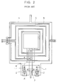
- DC SQUID which is shown in Fig. 2 in a top plan view, has a washer cover 8. Its operation was, however, unstable due to the lack of a ground plane, because interlinkage in external magnetic flux often occurred, which tended to invite trapping of magnetic flux. Because the trapping of interlinkage in magnet flux is generated in the neighborhood of the Josephson device 1, the operation in the prior art DC SQUID became unstable.
- a ground plane of superconducting layer is provided in such a manner that the ground plane overlays the area that contains the Josephson device.
- the number of processing steps does not have to be increased because this forming is simultaneously carried out with the same process in which the washer cover of the washer coil is processed. Since the DC SQUID in the foresaid structure is superconductively shielded by a ground plane in the neighborhood of the Josephson device, interlinkage of external magnetic flux can be avoided, and stable operation can then be realized without trapping external magnetic flux.
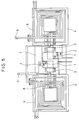
- Fig. 1 is a top plan view showing a DC SQUID as a first embodiment of the present invention.
- the DC SQUID operation becomes unstable in the manner that output signals flicker in its superconductivity state operation because magnetic flux becomes trapped or shifted. Such flicker becomes bigger in effect, especially in the case of trapping in the neighborhood of the Josephson device 1.
- the ground plane 7, which is an electrically insulated superconductive layer, covers broadly enough the area with the Josephson devices. Thus the traps of magnetic flux will hardly be generated, and the behavior becomes stable.
- the foresaid film should be as thick as the superconductive shielding, therefore, about 100 nm or more will be enough in case of Nb.
- the ground plane 7 may also be electrically grounded to the SQUID.
- the resistor films are insulated by means of an inter-layer insulating film 11, and the value of resistance should be fixed to a predetermined level.
- Said resistance film can be made of a metal such as Mo, MoN, Pd, Au, Cu, Al, Pd, Ti etc., any of which can be deposited by sputtering or evaporation.
- a 100 nm layer of Al should be deposited by DC magnetron sputtering and the pattern is then formed to the designed size by photolithography.
- both wet and dry etching methods can be used.
- wet etching there exists a method using a mixture of mainly phosphoric acid and nitric acid.
- dry etching there exists a method of reactive ion etching (RIE) using a chloride gas such as CCl4 or a mixture gas of the chloride gas.
- RIE reactive ion etching
- the inter-layer insulating film 11 can be made of SiO2, SiO, Si, MgO and the like. Any of these materials can be deposited by sputtering, evaporation or CVD and so on. The deposited film is set to be 1.5 to 2 times as thick as the resistance film, so as to insulate the resistance film completely. After a 100 to 200 nm thick SiO2 layer is deposited by RF magnetron sputtering, the SiO2 is etched to form contact holes to the resistance film by the photolithographic step. Both the wet and dry etching methods can be used for the etching of the SiO2. Wet etching is examplified by a method using a mixture of hydrofluoric acid.
- Dry etching is exemplified by reactive ion etching (i.e. RIE) using a mixture of CF4 or CHF3, and oxygen.
- RIE reactive ion etching
- the SiO2 is etched by the RIE method using a mixture of CHF3 and oxygen.
- the next step will be forming a Josephson device 1 comprising a lower electrode 12, a barrier layer 13, and an upper electrode 14, each of which should be deposited.
- the electrode 14 and the barrier layer 13 are etched by photolithography.
- the Josephson device 1 can be exemplified not only by the Nb/AlOx/Nb structure but also by a variety of structures of NbN/Mgo/NbN, Nb/Si/Nb, Nb/Nb-oxide/Nb and the like.
- the Nb/AlOx/Nb structure is deposited by a sputtering process.
- Examples of the deposition here are as follows. Ar gas is introduced into a reaction chamber, which is evacuated to a high vacuum of 10 ⁇ 5 Pa or less. And the Nb film of the lower electrode 12 is deposited under a pressure of 0.1 to 4 Pa by DC magnetron sputtering. The film is deposited to set to 100 to 300 nm in thickness. Then, the introduction of the argon gas is interrupted, and the reaction chamber is evacuated again to a high vacuum of 10 ⁇ 5 Pa or less.
- the argon gas is introduced so that the Al is deposited to 1 to 20 nm under a pressure of 0.1 to 4 Pa by DC magnetron sputtering. If the Al sputtering pressure is lower than that of Nb, the film becomes finer and this uniformity will be increased on the Nb surface. No problem arises here, even though the evacuation to a high vacuum is not elaborately performed before the sputtering of the Al.
- the reaction chamber is evacuated to a high vacuum of 10 ⁇ 5 Pa or less, and oxygen or a gas mixture of oxygen and argon is introduced to adjust the pressure to the set level. Then, the Al surface is oxidized to form the barrier layer 13 of AlOx/Al.
- the reaction chamber is evacuated to a high vacuum of 10 ⁇ 5 Pa or less, and the upper electrode 14 is deposited to 100 to 300 nm under the aforementioned Nb depositing condition.
- the upper electrode 14 and the barrier layer 13 are etched by a photolithographic step to form the Josephson device 1.
- the etching method used is generally a dry etching method using a plasma.
- the Nb of the upper electrode 14 is subjected to reactive ion etching (RIE) using CF4 or a gas mixture of CF4 and oxygen.
- RIE reactive ion etching
- the Al of the barrier layer 13 is removed by either the wet etching method using an acid or the RIE using Ar gas.
- the barrier layer 13 need not neccessarily be etched.
- the washer coil 4 is formed by patterning the superconductive film deposited as the lower electrode 12 of the Josephson device 1 by the photolithography.
- the etching method used is generally a dry etching method using plasma.
- the Nb of the lower electrode 12 is subjected to the plasma etching or reactive ion etching (RIE) using a gas mixture of CF4 and oxygen.
- RIE reactive ion etching
- the etching is so different from that of the aforementioned upper electrode 14 that isotropic etching is effected by increasing the amount of oxygen and that the resist film in the peripheral of the pattern is etched with oxygen into a tapered shape.
- the etching can be specifically exemplified by using a plasma etching apparatus with gas, which is prepared by adding 10 % of oxygen to CF4, under a pressure of 133 Pa and with a power of 50 W.
- gas which is prepared by adding 10 % of oxygen to CF4, under a pressure of 133 Pa and with a power of 50 W.
- a contact hole is then formed by photolithography.
- a superconductive film is then deposited again to form a feedback modulation coil 6 and an input coil 5 by photolithography.
- the superconducting film is exemplified by Nb, NbN, Pb-In or Pb-In-Au which is deposited by sputtering or evaporation.
- Nb film is deposited to 250 - 600 nm by DC magnetron sputtering, just as the Josephson junction electrode is formed.
- the substrate Before this deposition, the substrate should be reversely sputtered using Ar gas so that the substrate forms a superconductive contact.
- the washer coil 4 and counter electrodes and other wirings are formed by photolithography.
- the etching of the above is by plasma etching like the forming of the forementioned lower electrode 12.
- the buffer metal 9 may be necessary for the superconductive contact on the pad 10.
- a 10 - 100 nm thick Au layer is deposited on the buffer metal by sputtering.
- the patterning for the above can be done easily by wet etching using acid and the like.
- a wet or a dry method can be applied.
- an organic solvent such as acetone and the like, alkaline detachment liquid, concentrated nitric acid, heated concentrated sulfuric acid, etc. is used.
- oxygen plasma or UV rays are used. Exfoliation can be done by the combination of one or both methods or one or several of the materials above.
- Table 1 shows an example of a set of design parameters for the fabrication of a SQUID, the shape of which is shown in Fig. 1, i.e. the first embodiment.
- Fig. 4 and Fig. 5 show examples of second and third embodiments with samples of double washer coil types with two washer coils.
- the output signals tend to flicker, since it detects even uniform magnetic fields of flux linkage which the washer coil links to. Since SQUIDs with two washer coils can cancel the uniform magnetic flux of each other, the flicker of their output signals becomes smaller, and their operation becomes more stable.
- Fig. 4 is an example of parallel connecting
- Fig. 5 is an example of serial connecting.
- Each double washer coil SQUID has two feedback modulation coils 6, and each such SQUID can be utilized in many different ways.
- feedback modulation purposes either one coil or both coils can be used.
- Two coils may be used in such a way that one is for feedback purposes and another for modulation purposes.
- another usage can be in that two coils are used only for modulation purposes, and in this case, the feedback function may be realized through the usage of a coupled detection coil which works not only for detection but also for feedback.
Landscapes
- Physics & Mathematics (AREA)
- Condensed Matter Physics & Semiconductors (AREA)
- General Physics & Mathematics (AREA)
- Superconductor Devices And Manufacturing Methods Thereof (AREA)
- Measuring Magnetic Variables (AREA)
Applications Claiming Priority (2)
| Application Number | Priority Date | Filing Date | Title |
|---|---|---|---|
| JP214246/92 | 1992-08-11 | ||
| JP4214246A JP2964112B2 (ja) | 1992-08-11 | 1992-08-11 | 直流駆動型超伝導量子干渉素子 |
Publications (2)
| Publication Number | Publication Date |
|---|---|
| EP0591641A1 true EP0591641A1 (de) | 1994-04-13 |
| EP0591641B1 EP0591641B1 (de) | 1997-04-16 |
Family
ID=16652598
Family Applications (1)
| Application Number | Title | Priority Date | Filing Date |
|---|---|---|---|
| EP93112517A Expired - Lifetime EP0591641B1 (de) | 1992-08-11 | 1993-08-04 | Gleichstrom supraleitendes Quanteninterferenz-Bauelement |
Country Status (5)
| Country | Link |
|---|---|
| US (1) | US5548130A (de) |
| EP (1) | EP0591641B1 (de) |
| JP (1) | JP2964112B2 (de) |
| CA (1) | CA2103634A1 (de) |
| DE (1) | DE69309834T2 (de) |
Cited By (4)
| Publication number | Priority date | Publication date | Assignee | Title |
|---|---|---|---|---|
| DE4433331A1 (de) * | 1994-09-19 | 1996-03-21 | Siemens Ag | Magnetfeldempfindliche SQUID-Sensoreinrichtung mit Flußtransformator unter Verwendung von Hoch-T¶c¶-Supraleitermaterial |
| WO1996009654A1 (en) * | 1994-09-21 | 1996-03-28 | Commonwealth Scientific And Industrial Research Organisation | A method and device for improving the performance of thin-film josephson devices in magnetic fields |
| EP0775917A3 (de) * | 1995-11-22 | 1997-10-08 | Seiko Instr Inc | Squidmagnetometer und zerstörungsfreies Prüfgerät |
| CN104377299A (zh) * | 2014-08-21 | 2015-02-25 | 中国科学院上海微系统与信息技术研究所 | 无磁屏蔽环境下抑制磁场干扰的squid器件的结构 |
Families Citing this family (18)
| Publication number | Priority date | Publication date | Assignee | Title |
|---|---|---|---|---|
| JP3518184B2 (ja) * | 1996-08-02 | 2004-04-12 | 株式会社日立製作所 | 検出コイル一体型squid |
| JP2000091653A (ja) * | 1998-09-07 | 2000-03-31 | Seiko Instruments Inc | 超伝導量子干渉素子 |
| US20030068832A1 (en) * | 2001-08-29 | 2003-04-10 | Yuri Koval | Submicron closed-form josephson junctions |
| EP1717593A2 (de) * | 2002-08-02 | 2006-11-02 | QEST Quantenelektronische Systeme GmbH | Magnetometer |
| US20070054809A1 (en) * | 2005-09-02 | 2007-03-08 | National Institute Of Information And Communications Tech., Inc. Administrative Agency | Superconducting structure, apparatus for processing superconducting structure, and method for processing superconducting structure |
| CN102790170B (zh) * | 2011-05-19 | 2014-11-05 | 宇能电科技股份有限公司 | 磁阻感测元件及其形成方法 |
| US9768371B2 (en) | 2012-03-08 | 2017-09-19 | D-Wave Systems Inc. | Systems and methods for fabrication of superconducting integrated circuits |
| JP6735619B2 (ja) * | 2016-07-20 | 2020-08-05 | 日本電子株式会社 | 磁気共鳴測定用検出コイルの製造方法 |
| WO2018144601A1 (en) | 2017-02-01 | 2018-08-09 | D-Wave Systems Inc. | Systems and methods for fabrication of superconducting integrated circuits |
| KR102217205B1 (ko) * | 2017-03-13 | 2021-02-18 | 구글 엘엘씨 | 적층된 양자 컴퓨팅 디바이스 내의 집적 회로 소자 |
| US20200152851A1 (en) | 2018-11-13 | 2020-05-14 | D-Wave Systems Inc. | Systems and methods for fabricating superconducting integrated circuits |
| US12102017B2 (en) | 2019-02-15 | 2024-09-24 | D-Wave Systems Inc. | Kinetic inductance for couplers and compact qubits |
| CN110649152A (zh) * | 2019-09-27 | 2020-01-03 | 江苏鲁汶仪器有限公司 | 一种铌基超导器件刻蚀方法 |
| JP7705393B2 (ja) | 2019-12-05 | 2025-07-09 | ディー-ウェイブ システムズ インコーポレイテッド | 超伝導集積回路を製造するためのシステム及び方法 |
| WO2021231224A1 (en) | 2020-05-11 | 2021-11-18 | D-Wave Systems Inc. | Kinetic inductance devices, methods for fabricating kinetic inductance devices, and articles employing the same |
| CN112038479B (zh) * | 2020-09-04 | 2022-06-24 | 中国科学院上海微系统与信息技术研究所 | 电感可调的超导量子器件及其制备方法 |
| CN112881772B (zh) * | 2020-12-31 | 2023-08-25 | 中国计量科学研究院 | Squid电流传感器以及制备方法 |
| US12392823B2 (en) | 2021-11-05 | 2025-08-19 | D-Wave Systems Inc. | Systems and methods for on-chip noise measurements |
Citations (2)
| Publication number | Priority date | Publication date | Assignee | Title |
|---|---|---|---|---|
| EP0063887A1 (de) * | 1981-04-09 | 1982-11-03 | Sperry Corporation | Verfahren zum Herstellen von integrierten Schaltkreisen mit Josephson-Kontakten |
| EP0501220A2 (de) * | 1991-02-26 | 1992-09-02 | Seiko Instruments Inc. | Verfahren zum Herstellen eines Gleichstrom-Squids |
Family Cites Families (7)
| Publication number | Priority date | Publication date | Assignee | Title |
|---|---|---|---|---|
| JPS61196587A (ja) * | 1985-02-26 | 1986-08-30 | Mitsubishi Electric Corp | 直流駆動型超伝導量子干渉素子 |
| DE3515237A1 (de) * | 1985-04-26 | 1986-10-30 | Siemens AG, 1000 Berlin und 8000 München | Vorrichtung zur messung schwacher magnetfelder mit wenigstens einem dc-squid |
| DE3769201D1 (de) * | 1986-05-21 | 1991-05-16 | Siemens Ag | Squid-magnetometer fuer eine vorrichtung zur messung schwacher magnetfelder. |
| US5218297A (en) * | 1988-02-05 | 1993-06-08 | Hitachi, Ltd. | Superconductive quantum interference device in high temperature environments having reduced inductance and improved thermal noise response |
| JPH01217981A (ja) * | 1988-02-26 | 1989-08-31 | Mitsubishi Electric Corp | 超電導量子干渉素子 |
| JPH04130676A (ja) * | 1990-09-20 | 1992-05-01 | Shimadzu Corp | 準平面型ジョセフソン接合素子を用いたdc―squid |
| JP2780473B2 (ja) * | 1990-09-20 | 1998-07-30 | 株式会社島津製作所 | Dc―squid素子およびその製造方法 |
-
1992
- 1992-08-11 JP JP4214246A patent/JP2964112B2/ja not_active Expired - Fee Related
-
1993
- 1993-08-04 EP EP93112517A patent/EP0591641B1/de not_active Expired - Lifetime
- 1993-08-04 DE DE69309834T patent/DE69309834T2/de not_active Expired - Fee Related
- 1993-08-09 CA CA002103634A patent/CA2103634A1/en not_active Abandoned
-
1994
- 1994-12-29 US US08/366,363 patent/US5548130A/en not_active Expired - Lifetime
Patent Citations (2)
| Publication number | Priority date | Publication date | Assignee | Title |
|---|---|---|---|---|
| EP0063887A1 (de) * | 1981-04-09 | 1982-11-03 | Sperry Corporation | Verfahren zum Herstellen von integrierten Schaltkreisen mit Josephson-Kontakten |
| EP0501220A2 (de) * | 1991-02-26 | 1992-09-02 | Seiko Instruments Inc. | Verfahren zum Herstellen eines Gleichstrom-Squids |
Non-Patent Citations (1)
| Title |
|---|
| FUJITSU-SCIENTIFIC AND TECHNICAL JOURNAL vol. 24, no. 1, 1988, KAWASAKI JP pages 47 - 52 S. OHARA ET AL * |
Cited By (7)
| Publication number | Priority date | Publication date | Assignee | Title |
|---|---|---|---|---|
| DE4433331A1 (de) * | 1994-09-19 | 1996-03-21 | Siemens Ag | Magnetfeldempfindliche SQUID-Sensoreinrichtung mit Flußtransformator unter Verwendung von Hoch-T¶c¶-Supraleitermaterial |
| DE4433331C2 (de) * | 1994-09-19 | 2002-06-20 | Siemens Ag | Magnetfeldempfindliche SQUID-Sensoreinrichtung mit Flußtransformator unter Verwendung von Hoch-T¶c¶-Supraleitermaterial |
| WO1996009654A1 (en) * | 1994-09-21 | 1996-03-28 | Commonwealth Scientific And Industrial Research Organisation | A method and device for improving the performance of thin-film josephson devices in magnetic fields |
| EP0775917A3 (de) * | 1995-11-22 | 1997-10-08 | Seiko Instr Inc | Squidmagnetometer und zerstörungsfreies Prüfgerät |
| US5854492A (en) * | 1995-11-22 | 1998-12-29 | Seiko Instruments Inc. | Superconducting quantum interference device fluxmeter and nondestructive inspection apparatus |
| CN104377299A (zh) * | 2014-08-21 | 2015-02-25 | 中国科学院上海微系统与信息技术研究所 | 无磁屏蔽环境下抑制磁场干扰的squid器件的结构 |
| CN104377299B (zh) * | 2014-08-21 | 2017-09-26 | 中国科学院上海微系统与信息技术研究所 | 无磁屏蔽环境下抑制磁场干扰的squid器件的结构 |
Also Published As
| Publication number | Publication date |
|---|---|
| JPH0661536A (ja) | 1994-03-04 |
| DE69309834D1 (de) | 1997-05-22 |
| EP0591641B1 (de) | 1997-04-16 |
| JP2964112B2 (ja) | 1999-10-18 |
| US5548130A (en) | 1996-08-20 |
| CA2103634A1 (en) | 1994-02-12 |
| DE69309834T2 (de) | 1997-07-24 |
Similar Documents
| Publication | Publication Date | Title |
|---|---|---|
| EP0591641B1 (de) | Gleichstrom supraleitendes Quanteninterferenz-Bauelement | |
| US4386361A (en) | Thin film SQUID with low inductance | |
| EP3577700B1 (de) | Systeme und verfahren zur herstellung von supraleitenden integrierten schaltungen | |
| EP0501220B2 (de) | Verfahren zum Herstellen eines Gleichstrom-Squids | |
| US7247603B2 (en) | Charge dissipative dielectric for cryogenic devices | |
| Eidelloth et al. | YBa2Cu3O7− δ thin‐film gradiometers: Fabrication and performance | |
| EP0538077B1 (de) | Supraleitende Quanteninterferenz-Einrichtung | |
| JPS59138390A (ja) | 超電導スイツチング装置 | |
| EP0419361B2 (de) | Verfahren zur Herstellung einer Elektrode zur elektrischen Kontaktierung eines Oxyd-Supraleiters | |
| JPH0766462A (ja) | 超伝導回路 | |
| Yamasaki et al. | Design and fabrication of multichannel dc SQUIDs for biomagnetic applications | |
| EP0381541B1 (de) | Supraleitende magnetoresistive Anordnung | |
| Shimizu et al. | Performance of DC SQUIDs fabricated on 4-inch silicon wafer | |
| JPH07263761A (ja) | シールド付超伝導回路 | |
| JP3267352B2 (ja) | 超伝導量子干渉型デバイス及びその製造方法 | |
| JPH0555646A (ja) | 高感度磁場検出回路 | |
| JPH0669557A (ja) | 高感度磁場検出回路 | |
| EP0483741A2 (de) | Squid mit Polymer-Isolation | |
| JP3267353B2 (ja) | サブミクロン面積のエッジ接合を利用した弱接合型ジョセフソン素子の製造方法 | |
| JPH0766461A (ja) | 超伝導回路 | |
| KR960014974B1 (ko) | 초전도양자 간섭형 디바이스 및 그 제조방법 | |
| JPH04116989A (ja) | Squidおよびその製造方法 | |
| JPH04267569A (ja) | トンネル型ジョセフソン素子 | |
| JPH05175560A (ja) | 超電導量子干渉素子 | |
| JPS61260686A (ja) | ジヨセフソン集積回路 |
Legal Events
| Date | Code | Title | Description |
|---|---|---|---|
| PUAI | Public reference made under article 153(3) epc to a published international application that has entered the european phase |
Free format text: ORIGINAL CODE: 0009012 |
|
| AK | Designated contracting states |
Kind code of ref document: A1 Designated state(s): DE GB IT NL |
|
| 17P | Request for examination filed |
Effective date: 19941011 |
|
| 17Q | First examination report despatched |
Effective date: 19950628 |
|
| GRAG | Despatch of communication of intention to grant |
Free format text: ORIGINAL CODE: EPIDOS AGRA |
|
| RAP1 | Party data changed (applicant data changed or rights of an application transferred) |
Owner name: SEIKO INSTRUMENTS INC. |
|
| GRAH | Despatch of communication of intention to grant a patent |
Free format text: ORIGINAL CODE: EPIDOS IGRA |
|
| GRAH | Despatch of communication of intention to grant a patent |
Free format text: ORIGINAL CODE: EPIDOS IGRA |
|
| GRAA | (expected) grant |
Free format text: ORIGINAL CODE: 0009210 |
|
| AK | Designated contracting states |
Kind code of ref document: B1 Designated state(s): DE GB IT NL |
|
| REF | Corresponds to: |
Ref document number: 69309834 Country of ref document: DE Date of ref document: 19970522 |
|
| PLBE | No opposition filed within time limit |
Free format text: ORIGINAL CODE: 0009261 |
|
| 26N | No opposition filed | ||
| REG | Reference to a national code |
Ref country code: GB Ref legal event code: IF02 |
|
| REG | Reference to a national code |
Ref country code: GB Ref legal event code: 732E |
|
| NLS | Nl: assignments of ep-patents |
Owner name: SII NANOTECHNOLOGY INC. |
|
| PG25 | Lapsed in a contracting state [announced via postgrant information from national office to epo] |
Ref country code: IT Free format text: LAPSE BECAUSE OF NON-PAYMENT OF DUE FEES;WARNING: LAPSES OF ITALIAN PATENTS WITH EFFECTIVE DATE BEFORE 2007 MAY HAVE OCCURRED AT ANY TIME BEFORE 2007. THE CORRECT EFFECTIVE DATE MAY BE DIFFERENT FROM THE ONE RECORDED. Effective date: 20050804 |
|
| PGFP | Annual fee paid to national office [announced via postgrant information from national office to epo] |
Ref country code: GB Payment date: 20070801 Year of fee payment: 15 |
|
| PGFP | Annual fee paid to national office [announced via postgrant information from national office to epo] |
Ref country code: NL Payment date: 20070805 Year of fee payment: 15 |
|
| PGFP | Annual fee paid to national office [announced via postgrant information from national office to epo] |
Ref country code: DE Payment date: 20080814 Year of fee payment: 16 |
|
| GBPC | Gb: european patent ceased through non-payment of renewal fee |
Effective date: 20080804 |
|
| NLV4 | Nl: lapsed or anulled due to non-payment of the annual fee |
Effective date: 20090301 |
|
| PG25 | Lapsed in a contracting state [announced via postgrant information from national office to epo] |
Ref country code: NL Free format text: LAPSE BECAUSE OF NON-PAYMENT OF DUE FEES Effective date: 20090301 |
|
| PG25 | Lapsed in a contracting state [announced via postgrant information from national office to epo] |
Ref country code: GB Free format text: LAPSE BECAUSE OF NON-PAYMENT OF DUE FEES Effective date: 20080804 |
|
| PG25 | Lapsed in a contracting state [announced via postgrant information from national office to epo] |
Ref country code: DE Free format text: LAPSE BECAUSE OF NON-PAYMENT OF DUE FEES Effective date: 20100302 |