EP0591675A1 - Dispositif permettant d'éviter les décharges en arc dans les installations de pulvérisation sous vide - Google Patents
Dispositif permettant d'éviter les décharges en arc dans les installations de pulvérisation sous vide Download PDFInfo
- Publication number
- EP0591675A1 EP0591675A1 EP93113713A EP93113713A EP0591675A1 EP 0591675 A1 EP0591675 A1 EP 0591675A1 EP 93113713 A EP93113713 A EP 93113713A EP 93113713 A EP93113713 A EP 93113713A EP 0591675 A1 EP0591675 A1 EP 0591675A1
- Authority
- EP
- European Patent Office
- Prior art keywords
- cathode
- power supply
- voltage source
- pulse
- potential
- Prior art date
- Legal status (The legal status is an assumption and is not a legal conclusion. Google has not performed a legal analysis and makes no representation as to the accuracy of the status listed.)
- Granted
Links
Images
Classifications
-
- H—ELECTRICITY
- H01—ELECTRIC ELEMENTS
- H01J—ELECTRIC DISCHARGE TUBES OR DISCHARGE LAMPS
- H01J37/00—Discharge tubes with provision for introducing objects or material to be exposed to the discharge, e.g. for the purpose of examination or processing thereof
- H01J37/32—Gas-filled discharge tubes
- H01J37/34—Gas-filled discharge tubes operating with cathodic sputtering
-
- H—ELECTRICITY
- H01—ELECTRIC ELEMENTS
- H01J—ELECTRIC DISCHARGE TUBES OR DISCHARGE LAMPS
- H01J2237/00—Discharge tubes exposing object to beam, e.g. for analysis treatment, etching, imaging
- H01J2237/02—Details
- H01J2237/0203—Protection arrangements
- H01J2237/0206—Extinguishing, preventing or controlling unwanted discharges
Definitions
- the invention relates to a device according to the preamble of patent claim 1.
- the object of the invention is therefore to simplify the polarity reversal of an electrode in a direct current sputtering system in which electrically non-conductive substrates can also be coated or etched.
- the advantage achieved by the invention is in particular that the substrate-independent internal arcing is suppressed.
- the plasma feeding, i.e. energy supply is not pulsed, but a direct current supply.
- Such a power supply is simple and inexpensive, since there is no need for the complex switch that is necessary for pulse operation.
- the pulse current source used for "internal arcing" does not supply the plasma with any energy. Rather, it leads to an interruption of the coating process due to its opposite polarity.
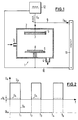
- FIG. 1 shows an atomization or sputtering system 1 which has a housing 2 which is provided with a gas inlet connector 3 and a gas outlet connector 4.
- a cathode 5 and an anode 6 lie opposite one another in the housing 2.
- the cathode 5 is cup-shaped and comprises a target 7, from which particles are knocked out during operation.
- the treatment may consist of coating or etching the substrate 8 out of the plasma.
- the cathode 5 is connected via a line 9 to the negative potential of a power supply 11, while the anode is connected to the positive potential of this power supply 11 via a line 10.
- the cathode 5 is also connected to a pulse current source 12, the output potential of which overlaps the negative potential of the power supply 11.
- FIG. 2 shows in more detail what the potential profile at the cathode 5 is.
- a pulse-shaped voltage U P from the pulse current source 12 is superimposed on the negative DC voltage potential U KO of the power supply 11.
- This pulse-shaped voltage U P is shown above the t-axis as it comes from the pulse current source 12, ie without superimposition.
- the resulting cathode voltage U K is shown in dashed lines in FIG. 2. It can be seen from this that the negative potential of the power supply 11 at the cathode 5 is brought to positive potential from time to time. For example, there is a negative potential U KO at the cathode 5 during the time T 1 - T 2, in order then to lie between T 2 and T 3 at a positive potential.
- the pulse-shaped voltages from the pulse current source 12 have a positive amplitude which is larger by an amount ⁇ U K than the negative amplitude of the direct voltage U KO . This results in an overall positive voltage of the size ⁇ U K at the cathode 5 during the time T2 to T3. This voltage causes the mentioned small capacitors to discharge at the target, so that a breakdown of these capacitors and thus also a flashover is prevented becomes.
- the location of a pulse e.g. B. T3 - T2 is z. B. less than 100 microseconds, while the time between two pulses is 100 to 1000 times thereof.
- the width and spacing of the pulses from the pulse current source 12 can be chosen as desired.
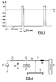
- FIG. 3 shows the superimposed cathode voltage U K with concrete time and amplitude values. It can clearly be seen here that the positive voltage pulses only occur for a relatively short time.
- Fig. 4 shows more details about the pulse control.
- a choke 20 is connected between the power supply 11 and the cathode 5, which among other things. current limitation.
- the pulse generator itself is designed as a controller 21, which closes and opens a switch 22 in a predetermined cycle and in this case gives the voltage of a DC voltage source 23 to the electrode 5 via a resistor 24 or keeps it away from the latter. It is understood that the controller 21 can be designed so that the pulse-clock ratio can be set as desired.
- a capacitor parallel to the voltage source 23 is designed so that it supplies a voltage with the required amplitude.
- the switch 22 can be implemented as a tube, thyristor or transistor.
Landscapes
- Physics & Mathematics (AREA)
- Engineering & Computer Science (AREA)
- Plasma & Fusion (AREA)
- Chemical & Material Sciences (AREA)
- Analytical Chemistry (AREA)
- Physical Vapour Deposition (AREA)
- Plasma Technology (AREA)
- Catching Or Destruction (AREA)
- Electrostatic Spraying Apparatus (AREA)
Applications Claiming Priority (2)
| Application Number | Priority Date | Filing Date | Title |
|---|---|---|---|
| DE4233720 | 1992-10-07 | ||
| DE4233720A DE4233720C2 (de) | 1992-10-07 | 1992-10-07 | Einrichtung für die Verhinderung von Überschlägen in Vakuum-Zerstäubungsanlagen |
Publications (2)
| Publication Number | Publication Date |
|---|---|
| EP0591675A1 true EP0591675A1 (fr) | 1994-04-13 |
| EP0591675B1 EP0591675B1 (fr) | 1996-07-24 |
Family
ID=6469856
Family Applications (1)
| Application Number | Title | Priority Date | Filing Date |
|---|---|---|---|
| EP93113713A Expired - Lifetime EP0591675B1 (fr) | 1992-10-07 | 1993-08-27 | Dispositif permettant d'éviter les décharges en arc dans les installations de pulvérisation sous vide |
Country Status (5)
| Country | Link |
|---|---|
| US (1) | US6440281B1 (fr) |
| EP (1) | EP0591675B1 (fr) |
| JP (1) | JP3516305B2 (fr) |
| DE (2) | DE4233720C2 (fr) |
| ES (1) | ES2094433T3 (fr) |
Cited By (12)
| Publication number | Priority date | Publication date | Assignee | Title |
|---|---|---|---|---|
| EP0692550A1 (fr) * | 1994-06-17 | 1996-01-17 | Eni, A Division Of Astec America, Inc. | Enlèvement d'isolants sur des cibles conductrices par pulvérisation cathodique préferentielle |
| US5576939A (en) * | 1995-05-05 | 1996-11-19 | Drummond; Geoffrey N. | Enhanced thin film DC plasma power supply |
| DE19610012A1 (de) * | 1996-03-14 | 1997-09-18 | Leybold Ag | Anordnung zum Beschichten eines Substrats mittels einer Sputtervorrichtung |
| EP0809275A1 (fr) * | 1996-05-24 | 1997-11-26 | Sekisui Chemical Co., Ltd. | Methode et appareil pour le traitement à plasma |
| WO1998054749A1 (fr) * | 1997-05-28 | 1998-12-03 | Advanced Energy Industries, Inc. | Depot en continu de materiau isolant au moyen d'anodes multiples a alternance entre tension positive et tension negative |
| US6001224A (en) * | 1993-04-02 | 1999-12-14 | Advanced Energy Industries, Inc. | Enhanced reactive DC sputtering system |
| US6007879A (en) * | 1995-04-07 | 1999-12-28 | Advanced Energy Industries, Inc. | Adjustable energy quantum thin film plasma processing system |
| EP0628212B1 (fr) * | 1992-12-30 | 2000-08-16 | Advanced Energy Industries, Inc. | Alimentation en courant continu pour reacteur a plasma |
| US6120656A (en) * | 1992-09-30 | 2000-09-19 | Advanced Energy Industries, Inc. | Topographically precise thin film coating system |
| US6217717B1 (en) | 1992-12-30 | 2001-04-17 | Advanced Energy Industries, Inc. | Periodically clearing thin film plasma processing system |
| DE10015244C2 (de) * | 2000-03-28 | 2002-09-19 | Fraunhofer Ges Forschung | Verfahren und Schaltungsanordnung zur pulsförmigen Energieeinspeisung in Magnetronentladungen |
| US6818103B1 (en) | 1999-10-15 | 2004-11-16 | Advanced Energy Industries, Inc. | Method and apparatus for substrate biasing in multiple electrode sputtering systems |
Families Citing this family (20)
| Publication number | Priority date | Publication date | Assignee | Title |
|---|---|---|---|---|
| DE19740793C2 (de) * | 1997-09-17 | 2003-03-20 | Bosch Gmbh Robert | Verfahren zur Beschichtung von Oberflächen mittels einer Anlage mit Sputterelektroden und Verwendung des Verfahrens |
| DE19826297A1 (de) * | 1998-06-12 | 1999-12-16 | Aurion Anlagentechnik Gmbh | Vorrichtung und Verfahren zur Vermeidung von Überschlägen bei Sputterprozessen durch eine aktive Arcunterdrückung |
| SE525231C2 (sv) * | 2001-06-14 | 2005-01-11 | Chemfilt R & D Ab | Förfarande och anordning för att alstra plasma |
| US9997338B2 (en) * | 2005-03-24 | 2018-06-12 | Oerlikon Surface Solutions Ag, Pfäffikon | Method for operating a pulsed arc source |
| US7305311B2 (en) * | 2005-04-22 | 2007-12-04 | Advanced Energy Industries, Inc. | Arc detection and handling in radio frequency power applications |
| US20080000768A1 (en) * | 2006-06-30 | 2008-01-03 | Stimson Bradley O | Electrically Coupled Target Panels |
| US8217299B2 (en) * | 2007-02-22 | 2012-07-10 | Advanced Energy Industries, Inc. | Arc recovery without over-voltage for plasma chamber power supplies using a shunt switch |
| KR101046520B1 (ko) | 2007-09-07 | 2011-07-04 | 어플라이드 머티어리얼스, 인코포레이티드 | 내부 챔버 상의 부산물 막 증착을 제어하기 위한 pecvd 시스템에서의 소스 가스 흐름 경로 제어 |
| DE112008002242B4 (de) * | 2007-09-25 | 2016-01-14 | Von Ardenne Gmbh | Verfahren und Anordnung zum redundanten Anoden-Sputtern mit einer Dual-Anoden-Anordnung |
| JP5500794B2 (ja) * | 2008-06-30 | 2014-05-21 | 株式会社アルバック | 電源装置 |
| JP5429772B2 (ja) * | 2008-06-30 | 2014-02-26 | 株式会社アルバック | 電源装置 |
| ATE535629T1 (de) * | 2008-07-29 | 2011-12-15 | Sulzer Metaplas Gmbh | Gepulstes hochleistungs-magnetronsputterverfahren sowie hochleistungs-elektroenergiequelle |
| US8044594B2 (en) * | 2008-07-31 | 2011-10-25 | Advanced Energy Industries, Inc. | Power supply ignition system and method |
| US8395078B2 (en) | 2008-12-05 | 2013-03-12 | Advanced Energy Industries, Inc | Arc recovery with over-voltage protection for plasma-chamber power supplies |
| EP2648209B1 (fr) | 2009-02-17 | 2018-01-03 | Solvix GmbH | Dispositif d'alimentation électrique pour le traitement au plasma |
| DE102010031568B4 (de) | 2010-07-20 | 2014-12-11 | TRUMPF Hüttinger GmbH + Co. KG | Arclöschanordnung und Verfahren zum Löschen von Arcs |
| US8552665B2 (en) | 2010-08-20 | 2013-10-08 | Advanced Energy Industries, Inc. | Proactive arc management of a plasma load |
| US20160268127A1 (en) * | 2015-03-13 | 2016-09-15 | Semiconductor Energy Laboratory Co., Ltd. | Oxide and Manufacturing Method Thereof |
| SG10201608814YA (en) | 2015-10-29 | 2017-05-30 | Semiconductor Energy Lab Co Ltd | Semiconductor device and method for manufacturing the semiconductor device |
| US10566177B2 (en) * | 2016-08-15 | 2020-02-18 | Applied Materials, Inc. | Pulse shape controller for sputter sources |
Citations (1)
| Publication number | Priority date | Publication date | Assignee | Title |
|---|---|---|---|---|
| US5015493A (en) * | 1987-01-11 | 1991-05-14 | Reinar Gruen | Process and apparatus for coating conducting pieces using a pulsed glow discharge |
Family Cites Families (5)
| Publication number | Priority date | Publication date | Assignee | Title |
|---|---|---|---|---|
| US4464223A (en) * | 1983-10-03 | 1984-08-07 | Tegal Corp. | Plasma reactor apparatus and method |
| US4693805A (en) * | 1986-02-14 | 1987-09-15 | Boe Limited | Method and apparatus for sputtering a dielectric target or for reactive sputtering |
| US5126033A (en) * | 1990-12-31 | 1992-06-30 | Leybold Aktiengesellschaft | Process and apparatus for reactively coating a substrate |
| DE4127317C2 (de) * | 1991-08-17 | 1999-09-02 | Leybold Ag | Einrichtung zum Behandeln von Substraten |
| DE4202425C2 (de) * | 1992-01-29 | 1997-07-17 | Leybold Ag | Verfahren und Vorrichtung zum Beschichten eines Substrats, insbesondere mit elektrisch nichtleitenden Schichten |
-
1992
- 1992-10-07 DE DE4233720A patent/DE4233720C2/de not_active Expired - Lifetime
-
1993
- 1993-08-27 EP EP93113713A patent/EP0591675B1/fr not_active Expired - Lifetime
- 1993-08-27 ES ES93113713T patent/ES2094433T3/es not_active Expired - Lifetime
- 1993-08-27 DE DE59303309T patent/DE59303309D1/de not_active Expired - Lifetime
- 1993-10-07 JP JP25196193A patent/JP3516305B2/ja not_active Expired - Fee Related
-
1995
- 1995-02-03 US US08/384,202 patent/US6440281B1/en not_active Expired - Fee Related
Patent Citations (1)
| Publication number | Priority date | Publication date | Assignee | Title |
|---|---|---|---|---|
| US5015493A (en) * | 1987-01-11 | 1991-05-14 | Reinar Gruen | Process and apparatus for coating conducting pieces using a pulsed glow discharge |
Cited By (24)
| Publication number | Priority date | Publication date | Assignee | Title |
|---|---|---|---|---|
| US6120656A (en) * | 1992-09-30 | 2000-09-19 | Advanced Energy Industries, Inc. | Topographically precise thin film coating system |
| US6217717B1 (en) | 1992-12-30 | 2001-04-17 | Advanced Energy Industries, Inc. | Periodically clearing thin film plasma processing system |
| EP0628212B1 (fr) * | 1992-12-30 | 2000-08-16 | Advanced Energy Industries, Inc. | Alimentation en courant continu pour reacteur a plasma |
| US6521099B1 (en) | 1992-12-30 | 2003-02-18 | Advanced Energy Industries, Inc. | Periodically clearing thin film plasma processing system |
| EP0692138B1 (fr) * | 1993-04-02 | 2004-01-21 | Advanced Energy Industries, Inc. | Systeme de pulverisation a courant continu provoquant une reaction chimique |
| US6001224A (en) * | 1993-04-02 | 1999-12-14 | Advanced Energy Industries, Inc. | Enhanced reactive DC sputtering system |
| EP0692550A1 (fr) * | 1994-06-17 | 1996-01-17 | Eni, A Division Of Astec America, Inc. | Enlèvement d'isolants sur des cibles conductrices par pulvérisation cathodique préferentielle |
| US5810982A (en) * | 1994-06-17 | 1998-09-22 | Eni Technologies, Inc. | Preferential sputtering of insulators from conductive targets |
| US5651865A (en) * | 1994-06-17 | 1997-07-29 | Eni | Preferential sputtering of insulators from conductive targets |
| US6368477B1 (en) | 1995-04-07 | 2002-04-09 | Advanced Energy Industries, Inc. | Adjustable energy quantum thin film plasma processing system |
| US6007879A (en) * | 1995-04-07 | 1999-12-28 | Advanced Energy Industries, Inc. | Adjustable energy quantum thin film plasma processing system |
| US5576939A (en) * | 1995-05-05 | 1996-11-19 | Drummond; Geoffrey N. | Enhanced thin film DC plasma power supply |
| DE19610012B4 (de) * | 1996-03-14 | 2005-02-10 | Unaxis Deutschland Holding Gmbh | Verfahren zur Stabilisierung eines Arbeitspunkts beim reaktiven Zerstäuben in einer Sauerstoff enthaltenden Atmosphäre |
| DE19610012A1 (de) * | 1996-03-14 | 1997-09-18 | Leybold Ag | Anordnung zum Beschichten eines Substrats mittels einer Sputtervorrichtung |
| EP0809275A1 (fr) * | 1996-05-24 | 1997-11-26 | Sekisui Chemical Co., Ltd. | Methode et appareil pour le traitement à plasma |
| US5968377A (en) * | 1996-05-24 | 1999-10-19 | Sekisui Chemical Co., Ltd. | Treatment method in glow-discharge plasma and apparatus thereof |
| EP1265268A1 (fr) * | 1996-05-24 | 2002-12-11 | Sekisui Chemical Co., Ltd. | Methode et appareil pour le traitement à plasma |
| WO1998054749A1 (fr) * | 1997-05-28 | 1998-12-03 | Advanced Energy Industries, Inc. | Depot en continu de materiau isolant au moyen d'anodes multiples a alternance entre tension positive et tension negative |
| US6183605B1 (en) | 1997-05-28 | 2001-02-06 | Advanced Energy Industries, Inc. | AC powered system for continuous deposition of a cathode material |
| EP1458006A1 (fr) * | 1997-05-28 | 2004-09-15 | Advanced Energy Industries, Inc. | Dépot continu de matériau isolant utilisant des anodes multiples connectées alternativement à des tensions positives et négatives |
| US5897753A (en) * | 1997-05-28 | 1999-04-27 | Advanced Energy Industries, Inc. | Continuous deposition of insulating material using multiple anodes alternated between positive and negative voltages |
| US6818103B1 (en) | 1999-10-15 | 2004-11-16 | Advanced Energy Industries, Inc. | Method and apparatus for substrate biasing in multiple electrode sputtering systems |
| US6522076B2 (en) | 2000-03-28 | 2003-02-18 | Fraunhofer-Gesellschaft zur Förderung der angewandten Forschung e.V. | Process and switching arrangement for pulsing energy introduction into magnetron discharges |
| DE10015244C2 (de) * | 2000-03-28 | 2002-09-19 | Fraunhofer Ges Forschung | Verfahren und Schaltungsanordnung zur pulsförmigen Energieeinspeisung in Magnetronentladungen |
Also Published As
| Publication number | Publication date |
|---|---|
| DE59303309D1 (de) | 1996-08-29 |
| DE4233720A1 (de) | 1994-04-14 |
| JP3516305B2 (ja) | 2004-04-05 |
| JPH06220629A (ja) | 1994-08-09 |
| DE4233720C2 (de) | 2001-05-17 |
| EP0591675B1 (fr) | 1996-07-24 |
| ES2094433T3 (es) | 1997-01-16 |
| US6440281B1 (en) | 2002-08-27 |
Similar Documents
| Publication | Publication Date | Title |
|---|---|---|
| EP0591675B1 (fr) | Dispositif permettant d'éviter les décharges en arc dans les installations de pulvérisation sous vide | |
| DE3733135C1 (de) | Vorrichtung zum Beschichten oder AEtzen mittels eines Plasmas | |
| DE4202425C2 (de) | Verfahren und Vorrichtung zum Beschichten eines Substrats, insbesondere mit elektrisch nichtleitenden Schichten | |
| EP0258296B1 (fr) | Dispositif de generation d'ions dans des courants de gaz | |
| DE68916938T2 (de) | Anordnung zum Abführen statischer Elektrizität von aufgeladenen Gegenständen in Reinräumen. | |
| DE19651811B4 (de) | Vorrichtung zum Belegen eines Substrats mit dünnen Schichten | |
| DE19702187C2 (de) | Verfahren und Einrichtung zum Betreiben von Magnetronentladungen | |
| EP0522281B1 (fr) | Procédé et dispositif d'allumage de plasmas en CVD | |
| DE3116732C2 (de) | Mit Hochfrequenzentladung arbeitende Zerstäubungsätzvorrichtung | |
| DE3005040C2 (fr) | ||
| DE2513216B2 (de) | Verfahren und Vorrichtung zur Beschichtung eines Substrats durch reaktive Kathodenzerstäubung | |
| DE2148933A1 (de) | HF-Zerstaeubungsvorrichtung | |
| DE4420951C2 (de) | Einrichtung zum Erfassen von Mikroüberschlägen in Zerstäubungsanlagen | |
| DE3705165A1 (de) | Mit entladungserregung arbeitende laservorrichtung fuer kurze impulse | |
| CH656818A5 (de) | Energiezuliefereinheit fuer eine funkenerosionsmaschine. | |
| DE4223505C1 (de) | Einrichtung zum aufbringen elektrisch schlecht leitender oder isolierender schichten durch reaktives magnetronsputtern | |
| EP1636403A2 (fr) | Installation de peinture electrophoretique par immersion | |
| DE4239218C2 (de) | Anordnung zum Verhindern von Überschlägen in einem Plasma-Prozeßraum | |
| DE1128063B (de) | Schaltanordnung fuer Elektro-Erosion mit pulsierendem Gleichstrom | |
| DE69109044T2 (de) | Vorrichtung zur Erzeugung und Umschaltung von hohen Spannungen an Röntgenröhren-Elektroden. | |
| DE4235766C2 (de) | Koronagenerator | |
| EP2637799A1 (fr) | Procédé pour le revêtement électrostatique d'objets ainsi que le dispositif d'application | |
| DE4436821A1 (de) | Funkengenerator sowie Verfahren zur Mikropartikel-Probenentnahme | |
| EP0607787A2 (fr) | Dispositif pour revêtir ou graver des substrats | |
| DE3791058C2 (de) | Verfahren und Vorrichtung zum Einbrennen von Elektronenröhren |
Legal Events
| Date | Code | Title | Description |
|---|---|---|---|
| PUAI | Public reference made under article 153(3) epc to a published international application that has entered the european phase |
Free format text: ORIGINAL CODE: 0009012 |
|
| AK | Designated contracting states |
Kind code of ref document: A1 Designated state(s): BE DE ES FR LU NL |
|
| 17P | Request for examination filed |
Effective date: 19940923 |
|
| 17Q | First examination report despatched |
Effective date: 19950731 |
|
| GRAH | Despatch of communication of intention to grant a patent |
Free format text: ORIGINAL CODE: EPIDOS IGRA |
|
| GRAA | (expected) grant |
Free format text: ORIGINAL CODE: 0009210 |
|
| AK | Designated contracting states |
Kind code of ref document: B1 Designated state(s): BE DE ES FR LU NL |
|
| REF | Corresponds to: |
Ref document number: 59303309 Country of ref document: DE Date of ref document: 19960829 |
|
| ET | Fr: translation filed | ||
| RAP2 | Party data changed (patent owner data changed or rights of a patent transferred) |
Owner name: BALZERS UND LEYBOLD DEUTSCHLAND HOLDING AKTIENGESE |
|
| NLT2 | Nl: modifications (of names), taken from the european patent patent bulletin |
Owner name: BALZERS UND LEYBOLD DEUTSCHLAND HOLDING AKTIENGESE |
|
| BECA | Be: change of holder's address |
Free format text: 960724 *BALZERS UND LEYBOLD DEUTSCHLAND HOLDING A.G.:WILHELM-ROHN-STRASSE 25, D-63450 HANAU |
|
| BECN | Be: change of holder's name |
Effective date: 19960724 |
|
| REG | Reference to a national code |
Ref country code: ES Ref legal event code: FG2A Ref document number: 2094433 Country of ref document: ES Kind code of ref document: T3 |
|
| NLT1 | Nl: modifications of names registered in virtue of documents presented to the patent office pursuant to art. 16 a, paragraph 1 |
Owner name: BALZERS UND LEYBOLD DEUTSCHLAND HOLDING AKTIENGESE |
|
| PLBE | No opposition filed within time limit |
Free format text: ORIGINAL CODE: 0009261 |
|
| 26N | No opposition filed | ||
| PGFP | Annual fee paid to national office [announced via postgrant information from national office to epo] |
Ref country code: ES Payment date: 20090820 Year of fee payment: 17 |
|
| PGFP | Annual fee paid to national office [announced via postgrant information from national office to epo] |
Ref country code: NL Payment date: 20090814 Year of fee payment: 17 Ref country code: LU Payment date: 20090820 Year of fee payment: 17 |
|
| PGFP | Annual fee paid to national office [announced via postgrant information from national office to epo] |
Ref country code: BE Payment date: 20090915 Year of fee payment: 17 |
|
| BERE | Be: lapsed |
Owner name: *BALZERS UND LEYBOLD DEUTSCHLAND HOLDING A.G. Effective date: 20100831 |
|
| REG | Reference to a national code |
Ref country code: NL Ref legal event code: V1 Effective date: 20110301 |
|
| PG25 | Lapsed in a contracting state [announced via postgrant information from national office to epo] |
Ref country code: NL Free format text: LAPSE BECAUSE OF NON-PAYMENT OF DUE FEES Effective date: 20110301 |
|
| PG25 | Lapsed in a contracting state [announced via postgrant information from national office to epo] |
Ref country code: BE Free format text: LAPSE BECAUSE OF NON-PAYMENT OF DUE FEES Effective date: 20100831 |
|
| REG | Reference to a national code |
Ref country code: ES Ref legal event code: FD2A Effective date: 20111019 |
|
| PG25 | Lapsed in a contracting state [announced via postgrant information from national office to epo] |
Ref country code: ES Free format text: LAPSE BECAUSE OF NON-PAYMENT OF DUE FEES Effective date: 20100828 |
|
| PG25 | Lapsed in a contracting state [announced via postgrant information from national office to epo] |
Ref country code: LU Free format text: LAPSE BECAUSE OF NON-PAYMENT OF DUE FEES Effective date: 20100827 |
|
| PGFP | Annual fee paid to national office [announced via postgrant information from national office to epo] |
Ref country code: FR Payment date: 20120906 Year of fee payment: 20 Ref country code: DE Payment date: 20120822 Year of fee payment: 20 |
|
| REG | Reference to a national code |
Ref country code: DE Ref legal event code: R071 Ref document number: 59303309 Country of ref document: DE |
|
| PG25 | Lapsed in a contracting state [announced via postgrant information from national office to epo] |
Ref country code: DE Free format text: LAPSE BECAUSE OF EXPIRATION OF PROTECTION Effective date: 20130828 |