EP0592205A1 - Halbleitermessaufnehmer mit Schaltung zur Feststellung von Fehlern - Google Patents
Halbleitermessaufnehmer mit Schaltung zur Feststellung von Fehlern Download PDFInfo
- Publication number
- EP0592205A1 EP0592205A1 EP93307931A EP93307931A EP0592205A1 EP 0592205 A1 EP0592205 A1 EP 0592205A1 EP 93307931 A EP93307931 A EP 93307931A EP 93307931 A EP93307931 A EP 93307931A EP 0592205 A1 EP0592205 A1 EP 0592205A1
- Authority
- EP
- European Patent Office
- Prior art keywords
- node
- comparator
- output
- bridge circuit
- inverted
- Prior art date
- Legal status (The legal status is an assumption and is not a legal conclusion. Google has not performed a legal analysis and makes no representation as to the accuracy of the status listed.)
- Granted
Links
Images


Classifications
-
- G—PHYSICS
- G01—MEASURING; TESTING
- G01P—MEASURING LINEAR OR ANGULAR SPEED, ACCELERATION, DECELERATION, OR SHOCK; INDICATING PRESENCE, ABSENCE, OR DIRECTION, OF MOVEMENT
- G01P21/00—Testing or calibrating of apparatus or devices covered by the preceding groups
-
- G—PHYSICS
- G01—MEASURING; TESTING
- G01L—MEASURING FORCE, STRESS, TORQUE, WORK, MECHANICAL POWER, MECHANICAL EFFICIENCY, OR FLUID PRESSURE
- G01L27/00—Testing or calibrating of apparatus for measuring fluid pressure
- G01L27/007—Malfunction diagnosis, i.e. diagnosing a sensor defect
Definitions
- This invention relates to a semiconductor sensor having a fault self-detecting circuit for detecting faults in the circuit components of the semiconductor sensor.
- a semiconductor sensor such as an acceleration sensor or a pressure sensor usually incorporates a lever or a thin film, aluminum wirings and resistor elements therein. These components are breakable, and the semiconductor sensor is usually equipped with a fault detecting circuit for warning the user of the fault.
- FIG.l of the- drawings A typical example of the fault detecting circuit incorporated in the semiconductor sensor is illustrated in Fig.l of the- drawings, and the fault detecting circuit aims at detection of a disconnection of the wiring, a disconnection of the resistor element and a breakage of the silicon thin film.
- the semiconductor sensor comprises a semiconductor thin film (not shown), a bridge circuit 1, a temperature compensating circuit 2 and a fault detecting circuit 3.
- the bridge circuit 1 is implemented by four resistor elements 1a, 1b, 1c and 1d, and is powered at power supply nodes P1 and P2.
- the semiconductor thin film is deformed, and the resistor elements unequally vary the resistor elements 1a to 1d.
- a potential difference is varied, and is taken out from a pair of output nodes OUT.
- the power node P1 is connected through the temperature compensating circuit 2 with a power supply terminal Vcc, and the other power node P2 is directly connected with a ground terminal.
- the temperature compensating circuit 2 has temperature characteristics inverse to the temperature characteristics of the bridge circuit 1, and modifies the power voltage level Vcc depending upon the environmental temperature. Therefore, the variation due to the temperature at the output nodes OUT is compensated by the variation of a driving voltage level Vb or the power voltage supplied from the temperature compensating circuit 2 to the bridge circuit 1, and the potential difference is exactly representative of the force exerted to the semiconductor thin film.
- the fault detecting circuit 3 comprises a series of resistor elements 3a and 3b connected between the power supply terminal Vcc and the ground terminal GND, and a comparator 3c.
- the resistor elements 3a and 3b produce a reference voltage signal Vref at the common node N1 thereof, and the reference voltage signal Vref is supplied to the inverted node of the comparator 3c.
- the output node N2 of the temperature compensating circuit 2 is connected with the non-inverted node of the comparator 3c, and the driving voltage level Vb is supplied to the comparator 3c.
- the comparator 3c compares the driving voltage level Vb with the reference voltage signal Vref, and produces the warning signal WRN when the driving voltage level Vb exceeds the reference voltage signal Vref.
- the temperature compensating circuit 2 is assumed to produce the driving voltage level Vb of 3 volts from Vcc at a standard temperature, and the temperature characteristics of the bridge circuit 1 is assumed to be equivalent to variation of the driving voltage level Vb at ⁇ 15% between -40 C° and +90C°.
- the temperature compensating circuit 2 is expected to change the driving voltage level between 2.53 volts and 3.45 volts. If the reference voltage signal Vref is regulated to 4.0 volts, the comparator 3c keeps the warning signal WRN inactive low as long as any fault does not take place.
- the driving voltage level Vb goes up as high as the power voltage level Vcc, and the non-inverted node becomes higher than the inverted node.
- the comparator 3c changes the warning signal WRN to the high voltage level, and informs the user of the fault.
- the fault detecting circuit monitors the driving voltage level Vb, and checks it whether or not a fault takes place.
- the prior art fault detecting circuit can find a disconnection between the power nodes P1 and P2.
- the fault detecting circuit also can not find the fault. Moreover, if the wiring between the bridge circuit 1 and either of the output terminals OUT is disconnected, the warning signal WRN does not warn the user or another device of the fault.
- the present invention provides a semiconductor sensor which is equipped with a fault detecting circuit effective against various faults of a Wheatstone bridge circuit. To achieve this end it independently monitors the output nodes of a Wheatstone bridge circuit to see whether or not the voltage levels at those output nodes remain in a normal voltage range.
- a semiconductor acceleration sensor embodying the present invention is fabricated on a semiconductor substrate 11.
- the semiconductor substrate 11 is partially etched away, and a weight portion 11a is supported through four beams 11b, 11c, 11d and 11e by a frame portion 11f.
- Impurity regions 11g, 11h, 11i and 11j of one conductivity type are formed in the beams 11b to 11e of the opposite conductivity type, and are connected with aluminum wiring strips 11k, 11m, 11n and 11o.
- the aluminum wiring strips 11k to 11o in turn are connected through aluminum wiring strips 11p, 11q, 11r and 11s with pads Pb, Ps1, Pgnd and Ps2, respectively.
- the impurity regions 11g to 11j serve as piezo resistor elements, and the aluminum wiring strips 11g to 11j and the aluminum wiring strips 11k to 11s are arranged to form a Wheatstone bridge circuit 12.
- the pad Pb and Pgnd serves as power nodes of the Wheatstone bridge circuit 12, and the pads Ps1 and Ps2 provide a pair of output nodes.
- the Wheatstone bridge circuit 12 changes the potential difference between the pad Ps1 and Ps2.
- the pad Pb of the Wheatstone bridge circuit 12 is connected through a temperature compensating circuit 13 with a power supply terminal Vcc, and the other pad Pgnd is directly connected with a ground terminal GND.
- the remaining pads Ps1 and Ps2 are connected with a pair of output terminals OUT as similar to the prior art semiconductor sensor.
- the temperature compensating circuit 13 behaves similar to that of the prior art semiconductor sensor 2, and supplies a driving voltage level Vb to the pad Pb of the Wheatstone bridge circuit 12.
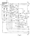
- a fault detecting circuit 14 is associated with the Wheatstone bridge circuit 12, and the fault detecting circuit 14 comprises a first comparator 14a, a second comparator 14b, a third comparator 14c, a fourth comparator 14d, a first reference voltage generator 14e, a first level-shifter 14f, a second reference voltage generator 14g and a second level-shifter 14h.
- the first comparator 14a is paired with the second comparator 14b for forming a first monitoring circuit 14i, and the output node Ps1 is connected with the inverted node of the first comparator 14a and the non-inverted node of the second comparator 14b.
- the first and second comparators 14a and 14b change the respective output signals from high voltage level to low voltage level.
- the comparators 14a and 14b thus arranged are referred to as "window comparators".
- the output nodes of the first and second comparators 14a and 14b are connected at a common node CN1, and the output signal Vc1 of the comparator 14a is ANDed with the output signal Vc2 of the comparator 14b.
- the third comparator 14c is paired with the fourth comparator 14d for forming a second monitoring circuit 14j
- the other output node Ps2 is connected with the inverted node of the third comparator 14c and the non-inverted node of the fourth comparator 14d.
- the third and fourth comparators 14c and 14d change the respective output signals from high voltage level to low voltage level, and, for this reason, the comparators 14c and 14d are also of the window comparator type.
- the output nodes of the third and fourth comparators 14c and 14d are connected at a common node CN2, and the output signal Vc3 of the comparator 14c is ANDed with the output signal Vc4 of the comparator 14d.
- the output nodes of all the comparators 14a to 14d are connected at a monitor node MNT.
- the first reference voltage generator 14e is implemented by a series of resistors R11, R12 and R13, and produces first and second reference voltages Vref11 and Vref12 at respective nodes N11 and N12 between the resistors R11 and R12 and between the resistors R12 and R13.
- the first and second reference voltages Vref11 and Vref12 are supplied to the non-inverted node of the first comparator 14a and the inverted node of the second comparator 14b, respectively.
- the first level-shifter 14f is implemented by a resistor R14 at least twentieth times larger in resistance than each of the resistor elements 11g to 11j, and is coupled between the output node Ps1 and a ground voltage line.
- the second reference voltage generator 14g is implemented by a series of resistors R15, R16 and R17, and produces third and fourth reference voltages Vref13 and Vref14 at respective nodes N13 and N14 between the resistors R15 and R16 and between the resistors R16 and R17.
- the third and fourth reference voltages Vref13 and Vref14 are supplied to the non-inverted node of the third comparator 14c and the inverted-node of the fourth comparator 14d, respectively.
- the second level-shifter 14h is implemented by a resistor R18 with extremely larger resistance than each of the resistor elements 11g to 11j, and is coupled between the output node Ps21 and the ground voltage line.
- the normal voltage range of the Wheatstone bridge circuit 12 is assumed to be a half of the driving voltage level Vb ⁇ 15 %. Since the driving voltage level Vb is adjusted to 3 volts at a standard temperature, and the normal voltage range is theoretically set to 1.5 volts ⁇ 225 millivolts, i.e., 1.275 volts to 1.725 volts. However, a margin should be taken into account, because the resistance of a resistor is not exactly adjusted to a target value. For this reason, the normal voltage range is set to 1.2 volts to 1.8 volts. In this situation, the output voltage signals Vc1 and Vc2 as well as the voltage level at the common node CN1 vary depending upon the voltage level at the output node Ps1 as shown in Table 1.
- two pairs of window comparators 14a to 14d are incorporated in the fault detecting circuit 12.
- the first and third comparators 14a and 14c monitor the output nodes Ps1 and Ps2 to see whether or not the voltage level thereat exceed the upper limit of the normal voltage range
- the second and fourth comparators 14b and 14d monitor the output nodes Ps1 and ps2 to see whether or not the voltage level thereat become lower than the lower limit of the normal voltage range.
- the window comparators 14a to 14d independently monitor the voltage level at the output nodes Ps1 and Ps2 to see whether or not the voltage levels thereat remain in the normal voltage range, and any abnormal voltage level at the output node Ps1 or PS2 results in a voltage shift at the monitor node MNT, because the window comparators 14a to 14d are ANDed with one another.
- the fault detecting circuit 14 produces and supplies a warning signal to the monitor node MNT.
- Table 2 illustrates detectable faults and the fault origins.
- the output node Ps1 discharges current through the resistor R14 to the ground voltage line, and becomes equal to the ground voltage level.
- the voltage level at the output node Ps1 is lower than the lower limit of the normal voltage range, and the comparators 14a and 14b supply the output signal Vc1 of the high level and the output signal Vc2 of the low level to the common node CN1, respectively.
- the output signal Vc1 is ANDed with the output signal Vc2, and the monitor node MNT is changed to the low level indicative of occurrence of the fault.
- the output node Ps1 goes up, and becomes equal to the driving voltage level Vb.
- the voltage level at the output node Ps1 exceeds the upper limit of the normal voltage range, and the first and second comparators 14a and 14b produce the output signal Vc1 of the low level and the output signal Vc2 of the high level.
- the output signal Vc1 is ANDed with the output signal Vc2, and the monitor node MNT is changed to the low level indicative of occurrence of the fault.
- the fault detecting circuit 14 changes the warning signal to the low level.
- the piezo resistor element is damaged, and the fault detecting circuit 14 changes the warning signal to the low level.
- one of the first to fourth comparators 14a to 14d detects the abnormal voltage, and shifts the warning signal to the low level indicative of occurrence of a fault.
- the present invention is applicable to any semiconductor sensor for converting a deformation of a component member into an electric signal
- a semiconductor pressure sensor and a vibration sensor are examples of the semiconductor sensors to which the present invention appertains.
- the structure of the semiconductor sensor is not limited to that shown in Fig. 2.
- the fault detecting circuit may be fabricated on a semiconductor substrate together with the bridge circuit and on a semiconductor substrate separated from the semiconductor substrate for the bridge circuit.
Landscapes
- Physics & Mathematics (AREA)
- General Physics & Mathematics (AREA)
- Health & Medical Sciences (AREA)
- Chemical & Material Sciences (AREA)
- Engineering & Computer Science (AREA)
- Analytical Chemistry (AREA)
- Biomedical Technology (AREA)
- Testing Of Short-Circuits, Discontinuities, Leakage, Or Incorrect Line Connections (AREA)
Applications Claiming Priority (2)
| Application Number | Priority Date | Filing Date | Title |
|---|---|---|---|
| JP268294/92 | 1992-10-07 | ||
| JP26829492 | 1992-10-07 |
Publications (2)
| Publication Number | Publication Date |
|---|---|
| EP0592205A1 true EP0592205A1 (de) | 1994-04-13 |
| EP0592205B1 EP0592205B1 (de) | 1998-01-07 |
Family
ID=17456534
Family Applications (1)
| Application Number | Title | Priority Date | Filing Date |
|---|---|---|---|
| EP93307931A Expired - Lifetime EP0592205B1 (de) | 1992-10-07 | 1993-10-06 | Halbleitermessaufnehmer mit Schaltung zur Feststellung von Fehlern |
Country Status (3)
| Country | Link |
|---|---|
| US (1) | US5440234A (de) |
| EP (1) | EP0592205B1 (de) |
| DE (1) | DE69316136T2 (de) |
Cited By (7)
| Publication number | Priority date | Publication date | Assignee | Title |
|---|---|---|---|---|
| GB2334588A (en) * | 1998-02-18 | 1999-08-25 | Telefunken Microelectron | Monitoring correct operation of a sensor module comprising a Wheatstone bridge circuit |
| EP0967462A1 (de) * | 1998-06-26 | 1999-12-29 | B. Braun Melsungen Ag | Brückensensor und Prüfverfahren |
| EP1087219A3 (de) * | 1999-09-24 | 2002-03-13 | Denso Corporation | System zum Bestimmen von Fehlern oder Abnormalitäten eines Messfühlers, eingebaut in ein Gerät zur Messung einer physikalischen oder dynamischen Grösse |
| EP1416286A2 (de) | 2002-10-22 | 2004-05-06 | Texas Instruments Incorporated | Wheatstonebrücke |
| EP1503184A3 (de) * | 2003-07-29 | 2005-10-26 | Alps Electric Co., Ltd. | Fehlererfassungsschaltung |
| EP1795903A3 (de) * | 2005-11-21 | 2008-10-01 | Fujitsu Ltd. | Vorrichtung zur Detektion eines Defekts in einem Sensor |
| EP4056957B1 (de) | 2021-03-10 | 2024-10-16 | Honeywell International Inc. | Offset-kalibrierung und diagnose für widerstandsbasierte brückenschaltungen |
Families Citing this family (24)
| Publication number | Priority date | Publication date | Assignee | Title |
|---|---|---|---|---|
| DE69425437T2 (de) * | 1994-05-30 | 2001-01-25 | Nagano Keiki Seisakusho Ltd., Tokio/Tokyo | Restdruckwandler |
| FR2732133B1 (fr) * | 1995-03-21 | 1997-04-25 | Sgs Thomson Microelectronics | Detecteur de coherence d'informations contenues dans un circuit integre |
| US5942900A (en) * | 1996-12-17 | 1999-08-24 | Lexmark International, Inc. | Method of fault detection in ink jet printhead heater chips |
| US5959537A (en) * | 1998-07-09 | 1999-09-28 | Mcgraw-Edison Company | Variable trip fault indicator |
| US6118278A (en) * | 1998-08-18 | 2000-09-12 | Hewlett-Packard Company | Short circuit detection in particular for a measuring bridge |
| US6177875B1 (en) * | 1999-09-28 | 2001-01-23 | Rockwell Technologies, Llc | Simple voltage window sensing circuit |
| US6433554B1 (en) * | 1999-12-20 | 2002-08-13 | Texas Instruments Incorporated | Method and apparatus for in-range fault detection of condition responsive sensor |
| JP2003214967A (ja) * | 2002-01-22 | 2003-07-30 | Hitachi Unisia Automotive Ltd | ブリッジ回路型検出素子 |
| DE102004056133B4 (de) * | 2004-02-20 | 2007-04-12 | Fraunhofer-Gesellschaft zur Förderung der angewandten Forschung e.V. | Verfahren zur Erfassung einer Offsetdrift bei einer Wheatstone-Meßbrücke |
| US7609158B2 (en) * | 2006-10-26 | 2009-10-27 | Cooper Technologies Company | Electrical power system control communications network |
| US7715002B2 (en) * | 2007-01-23 | 2010-05-11 | Bionorica Ag | Method for classifying scientific materials such as silicate materials, polymer materials and/or nanomaterials |
| US7930141B2 (en) | 2007-11-02 | 2011-04-19 | Cooper Technologies Company | Communicating faulted circuit indicator apparatus and method of use thereof |
| US9383394B2 (en) * | 2007-11-02 | 2016-07-05 | Cooper Technologies Company | Overhead communicating device |
| US8594956B2 (en) * | 2007-11-02 | 2013-11-26 | Cooper Technologies Company | Power line energy harvesting power supply |
| US8067946B2 (en) * | 2007-11-02 | 2011-11-29 | Cooper Technologies Company | Method for repairing a transmission line in an electrical power distribution system |
| US20090231764A1 (en) * | 2008-03-14 | 2009-09-17 | Cooper Technologies Company | Capacitor Bank Monitor and Method of use Thereof |
| JP5517777B2 (ja) * | 2010-06-25 | 2014-06-11 | 日立オートモティブシステムズ株式会社 | ブリッジ回路の断線検出回路および断線検出手段を有するシステム |
| CA2807295C (en) | 2010-08-10 | 2017-11-07 | Cooper Technologies Company | Apparatus and method for mounting an overhead device |
| DE212013000103U1 (de) * | 2012-04-20 | 2014-11-20 | Panasonic Intellectual Property Management Co., Ltd. | Trägheitskraftsensor |
| JP6049488B2 (ja) * | 2013-02-14 | 2016-12-21 | エスアイアイ・セミコンダクタ株式会社 | センサ回路 |
| US9379556B2 (en) | 2013-03-14 | 2016-06-28 | Cooper Technologies Company | Systems and methods for energy harvesting and current and voltage measurements |
| US9322732B2 (en) * | 2014-01-17 | 2016-04-26 | Hamilton Sundstrand Corporation | Strain gauge pressure sensor circuit with sensor disconnect detection |
| CN104880143B (zh) * | 2015-05-28 | 2017-12-26 | 西北工业大学 | 一种桥式电阻应变传感器多模态故障检测装置 |
| JP2021018075A (ja) * | 2019-07-17 | 2021-02-15 | 株式会社デンソー | センサ装置 |
Citations (2)
| Publication number | Priority date | Publication date | Assignee | Title |
|---|---|---|---|---|
| JPS63132171A (ja) * | 1986-11-21 | 1988-06-04 | Nippon Denso Co Ltd | 半導体式加速度検出装置 |
| EP0444866A1 (de) * | 1990-03-01 | 1991-09-04 | Airbag Systems Company Ltd | Steuerungssystem für eine Fahrzeugsicherheitsvorrichtung |
Family Cites Families (5)
| Publication number | Priority date | Publication date | Assignee | Title |
|---|---|---|---|---|
| US3818330A (en) * | 1972-08-17 | 1974-06-18 | Hitachi Ltd | Device having a bridge circuit for detecting faults in an electric network |
| US4250829A (en) * | 1978-05-30 | 1981-02-17 | Brunswick Corporation | Vapor detector for marine propulsion apparatus |
| US4956631A (en) * | 1989-03-20 | 1990-09-11 | Mitsubishi Denki Kabushiki Kaisha | Fault detector for vehicle safety system |
| JPH0742878Y2 (ja) * | 1989-04-14 | 1995-10-04 | 日本精工株式会社 | 乗員保護装置の故障検出装置 |
| JPH0818529B2 (ja) * | 1990-11-20 | 1996-02-28 | 三菱電機株式会社 | 乗員保護装置の故障検出装置 |
-
1993
- 1993-10-06 DE DE69316136T patent/DE69316136T2/de not_active Expired - Fee Related
- 1993-10-06 EP EP93307931A patent/EP0592205B1/de not_active Expired - Lifetime
- 1993-10-07 US US08/134,029 patent/US5440234A/en not_active Expired - Fee Related
Patent Citations (2)
| Publication number | Priority date | Publication date | Assignee | Title |
|---|---|---|---|---|
| JPS63132171A (ja) * | 1986-11-21 | 1988-06-04 | Nippon Denso Co Ltd | 半導体式加速度検出装置 |
| EP0444866A1 (de) * | 1990-03-01 | 1991-09-04 | Airbag Systems Company Ltd | Steuerungssystem für eine Fahrzeugsicherheitsvorrichtung |
Non-Patent Citations (1)
| Title |
|---|
| PATENT ABSTRACTS OF JAPAN vol. 12, no. 390 (P - 772) 18 October 1988 (1988-10-18) * |
Cited By (10)
| Publication number | Priority date | Publication date | Assignee | Title |
|---|---|---|---|---|
| GB2334588A (en) * | 1998-02-18 | 1999-08-25 | Telefunken Microelectron | Monitoring correct operation of a sensor module comprising a Wheatstone bridge circuit |
| EP0967462A1 (de) * | 1998-06-26 | 1999-12-29 | B. Braun Melsungen Ag | Brückensensor und Prüfverfahren |
| EP1087219A3 (de) * | 1999-09-24 | 2002-03-13 | Denso Corporation | System zum Bestimmen von Fehlern oder Abnormalitäten eines Messfühlers, eingebaut in ein Gerät zur Messung einer physikalischen oder dynamischen Grösse |
| US6422088B1 (en) | 1999-09-24 | 2002-07-23 | Denso Corporation | Sensor failure or abnormality detecting system incorporated in a physical or dynamic quantity detecting apparatus |
| EP1666862A3 (de) * | 1999-09-24 | 2006-12-20 | Denso Corporation | In ein physikalisches oder dynamisches Mengendetektionsgerät integriertes System für den Nachweis von Sensordefekten oder -fehlern |
| EP1416286A2 (de) | 2002-10-22 | 2004-05-06 | Texas Instruments Incorporated | Wheatstonebrücke |
| EP1416286A3 (de) * | 2002-10-22 | 2007-11-14 | Sensata Technologies, Inc. | Wheatstonebrücke |
| EP1503184A3 (de) * | 2003-07-29 | 2005-10-26 | Alps Electric Co., Ltd. | Fehlererfassungsschaltung |
| EP1795903A3 (de) * | 2005-11-21 | 2008-10-01 | Fujitsu Ltd. | Vorrichtung zur Detektion eines Defekts in einem Sensor |
| EP4056957B1 (de) | 2021-03-10 | 2024-10-16 | Honeywell International Inc. | Offset-kalibrierung und diagnose für widerstandsbasierte brückenschaltungen |
Also Published As
| Publication number | Publication date |
|---|---|
| DE69316136D1 (de) | 1998-02-12 |
| US5440234A (en) | 1995-08-08 |
| DE69316136T2 (de) | 1998-05-14 |
| EP0592205B1 (de) | 1998-01-07 |
Similar Documents
| Publication | Publication Date | Title |
|---|---|---|
| US5440234A (en) | Fault detecting circuit incorporated in semiconductor sensor and effective against any fault having influence on output voltage of a circuit component of the sensor | |
| US8330469B2 (en) | Battery voltage monitoring apparatus | |
| KR100944588B1 (ko) | 차량 내의 에어백 제어기 | |
| JPWO2007119682A1 (ja) | 電池パックおよびその断線検知方法 | |
| KR20030081042A (ko) | 단선 고장 검지 회로 | |
| JP5278114B2 (ja) | センサ装置 | |
| JP4316598B2 (ja) | 乗員検出装置 | |
| JPH06229778A (ja) | 故障検出回路付半導体センサ装置 | |
| JP4149440B2 (ja) | アナログセンサのための保護回路 | |
| US6696840B2 (en) | Device for triggering ignition circuits | |
| JP2001091385A (ja) | 断線検出機能付きブリッジセンサ | |
| JP7391720B2 (ja) | 半導体集積回路装置および電流検出回路 | |
| US9664753B2 (en) | Hall-effect-based magnetic field sensor having an improved output bandwidth | |
| JP2737481B2 (ja) | 半導体加速度センサー | |
| US12587003B2 (en) | On-board device | |
| JPWO2021124719A5 (de) | ||
| KR102275669B1 (ko) | 자기 센서 및 자기 센서 장치 | |
| JP3397042B2 (ja) | マイクロメカニカルセンサ破損検出回路 | |
| JPH02307064A (ja) | 半導体式加速度検出装置 | |
| JP2705426B2 (ja) | 加速度センサ | |
| JP2001091384A (ja) | 断線検出機能付きブリッジセンサ | |
| JP2024073681A (ja) | 信号出力回路及び半導体集積回路装置 | |
| JPH087692Y2 (ja) | センサ信号処理回路 | |
| CN119301725A (zh) | 直流短路保护装置 | |
| JPH10160753A (ja) | 加速度センサ |
Legal Events
| Date | Code | Title | Description |
|---|---|---|---|
| PUAI | Public reference made under article 153(3) epc to a published international application that has entered the european phase |
Free format text: ORIGINAL CODE: 0009012 |
|
| 17P | Request for examination filed |
Effective date: 19940201 |
|
| AK | Designated contracting states |
Kind code of ref document: A1 Designated state(s): DE FR GB NL |
|
| 17Q | First examination report despatched |
Effective date: 19960508 |
|
| GRAG | Despatch of communication of intention to grant |
Free format text: ORIGINAL CODE: EPIDOS AGRA |
|
| GRAH | Despatch of communication of intention to grant a patent |
Free format text: ORIGINAL CODE: EPIDOS IGRA |
|
| GRAH | Despatch of communication of intention to grant a patent |
Free format text: ORIGINAL CODE: EPIDOS IGRA |
|
| GRAA | (expected) grant |
Free format text: ORIGINAL CODE: 0009210 |
|
| AK | Designated contracting states |
Kind code of ref document: B1 Designated state(s): DE FR GB NL |
|
| REF | Corresponds to: |
Ref document number: 69316136 Country of ref document: DE Date of ref document: 19980212 |
|
| ET | Fr: translation filed | ||
| PLBE | No opposition filed within time limit |
Free format text: ORIGINAL CODE: 0009261 |
|
| 26N | No opposition filed | ||
| REG | Reference to a national code |
Ref country code: GB Ref legal event code: IF02 |
|
| PGFP | Annual fee paid to national office [announced via postgrant information from national office to epo] |
Ref country code: GB Payment date: 20021002 Year of fee payment: 10 |
|
| PGFP | Annual fee paid to national office [announced via postgrant information from national office to epo] |
Ref country code: FR Payment date: 20021008 Year of fee payment: 10 |
|
| PGFP | Annual fee paid to national office [announced via postgrant information from national office to epo] |
Ref country code: DE Payment date: 20021011 Year of fee payment: 10 |
|
| PGFP | Annual fee paid to national office [announced via postgrant information from national office to epo] |
Ref country code: NL Payment date: 20021031 Year of fee payment: 10 |
|
| PG25 | Lapsed in a contracting state [announced via postgrant information from national office to epo] |
Ref country code: GB Free format text: LAPSE BECAUSE OF NON-PAYMENT OF DUE FEES Effective date: 20031006 |
|
| PG25 | Lapsed in a contracting state [announced via postgrant information from national office to epo] |
Ref country code: NL Free format text: LAPSE BECAUSE OF NON-PAYMENT OF DUE FEES Effective date: 20040501 Ref country code: DE Free format text: LAPSE BECAUSE OF NON-PAYMENT OF DUE FEES Effective date: 20040501 |
|
| GBPC | Gb: european patent ceased through non-payment of renewal fee |
Effective date: 20031006 |
|
| PG25 | Lapsed in a contracting state [announced via postgrant information from national office to epo] |
Ref country code: FR Free format text: LAPSE BECAUSE OF NON-PAYMENT OF DUE FEES Effective date: 20040630 |
|
| NLV4 | Nl: lapsed or anulled due to non-payment of the annual fee |
Effective date: 20040501 |
|
| REG | Reference to a national code |
Ref country code: FR Ref legal event code: ST |