EP0593686B1 - Steuerverfahren fuer ein quasiresonanter spannungs-wechselrichter - Google Patents
Steuerverfahren fuer ein quasiresonanter spannungs-wechselrichter Download PDFInfo
- Publication number
- EP0593686B1 EP0593686B1 EP92919203A EP92919203A EP0593686B1 EP 0593686 B1 EP0593686 B1 EP 0593686B1 EP 92919203 A EP92919203 A EP 92919203A EP 92919203 A EP92919203 A EP 92919203A EP 0593686 B1 EP0593686 B1 EP 0593686B1
- Authority
- EP
- European Patent Office
- Prior art keywords
- voltage
- quasi
- resonance
- regulating
- capacitor
- Prior art date
- Legal status (The legal status is an assumption and is not a legal conclusion. Google has not performed a legal analysis and makes no representation as to the accuracy of the status listed.)
- Expired - Lifetime
Links
Images


Classifications
-
- H—ELECTRICITY
- H02—GENERATION; CONVERSION OR DISTRIBUTION OF ELECTRIC POWER
- H02M—APPARATUS FOR CONVERSION BETWEEN AC AND AC, BETWEEN AC AND DC, OR BETWEEN DC AND DC, AND FOR USE WITH MAINS OR SIMILAR POWER SUPPLY SYSTEMS; CONVERSION OF DC OR AC INPUT POWER INTO SURGE OUTPUT POWER; CONTROL OR REGULATION THEREOF
- H02M7/00—Conversion of AC power input into DC power output; Conversion of DC power input into AC power output
- H02M7/42—Conversion of DC power input into AC power output without possibility of reversal
- H02M7/44—Conversion of DC power input into AC power output without possibility of reversal by static converters
- H02M7/48—Conversion of DC power input into AC power output without possibility of reversal by static converters using discharge tubes with control electrode or semiconductor devices with control electrode
- H02M7/4826—Conversion of DC power input into AC power output without possibility of reversal by static converters using discharge tubes with control electrode or semiconductor devices with control electrode operating from a resonant DC source, i.e. the DC input voltage varies periodically, e.g. resonant DC-link inverters
Definitions
- the present invention relates to voltage inverters operating in quasi-resonance.
- inverters are supplied by a DC voltage source, they include a bridge, single-phase or multi-phase, with controlled components operating in blocked-saturated mode; these inverters comprise an oscillating circuit arranged on the side of the DC voltage supply; it consists of an inductor in series with the DC voltage source and a capacitor connected in parallel on the controlled rectifier bridge.
- any switching of any one of the controlled components of the bridge must coincide substantially with the zero crossing of the voltage across the capacitors of the oscillating circuit.
- Resonance converters supplied by a DC voltage source are described in the CONF REC IEEE Industry Applications Society Annual Meeting article, vol. II, October 1990, Seattle Washington US, pages 984-990 of Venkataramanan & Divan entitled "Pulse Width Modulation with Resonant DC Link Converters" as well as in the CONF REC article IEEE Industry Applications Society Annual Meeting, vol. I, October 1989, San Diego California US, pages 1037-1044, from Tenti, Divan & Toigo entitled "A synchronized Resonant DC Link Converter for Soft-Switched PWM”.
- JP-A-13 18 547 further describes a device for controlling the switching of a power source comprising a converter of the resonance type, a pulse width control circuit, a rectifier circuit, an oscillator, a synchronous circuit and a gate circuit.
- the present invention therefore aims to provide a voltage inverter operating in quasi-resonance in which the switching losses are significantly reduced and which can be subject to digital regulations efficient for controlling various loads of the inverter.
- the invention as defined in claim 1 relates to a pulse width modulation regulation method by means of a digital regulator of a voltage inverter operating in quasi-resonance, comprising a bridge. of controlled rectifiers operating in blocked-saturated mode and an oscillating circuit arranged on the DC side and consisting of an inductor in series with the DC source and of a capacitor connected in parallel on the bridge of controlled rectifiers, characterized in that that the sampling period of the digital regulator is equal to approximately ten times or more the resonance period of the oscillating circuit.
- the invention makes it possible to separate the holding function, by analog means, at high frequency. short circuits necessary for the maintenance of the oscillation, of the regulation function proper. This allows the use of digital regulators operating at frequencies lower than the resonant frequency and which can take account of the characteristics of the load.
- the invention therefore makes it possible to combine the advantages specific to high frequency resonance, namely the reduction in volume and the efficiency, with those of digital controls, namely processing flexibility, adaptability and optimization.
- the voltage pulses imposed by the output of the regulation consist of a series of periods of sinusoids at the resonance frequency. These pulses are positioned only at discrete instants which correspond to the passage through zero of the voltage across the terminals of the capacitor which is in parallel on the bridge.
- this limiter limits the voltage across the capacitor, during switching operations, to a voltage slightly greater than twice the direct supply voltage, E.
- Figure 1 is the diagram of a conventional voltage inverter operating in quasi-resonance.
- a source of direct voltage 1, of voltage E supplies a bridge with controlled components 3 operating in blocked-saturated mode, that is to say with controlled ignition and extinction; a freewheeling diode 4 is arranged in parallel on each of the controlled components 3.
- the quasi-resonance operation is obtained thanks to an oscillating circuit arranged on the DC voltage side; it consists of an inductor 5 in series with the DC voltage source 1 and of a capacitor 6 in parallel on the bridge 2.
- the load 8 which must be supplied, by voltage waves so as to be traversed by a sinusoidal alternating current, is arranged between two points located between the components controlled on each of the arms of the inverter.
- a clipping device 7 is connected in parallel to the capacitor 6. This clipper limits the voltage across the capacitor to a value slightly greater than twice the voltage, E, of the DC voltage source 1.
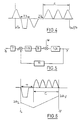
- FIG. 2 illustrates the principle of the method according to the invention.
- the regulation of the alternating current supplied by the inverter is carried out by a conventional pulse width modulation method with a regular sampling period Te much greater than and approximately of the order of at least ten times or more the period of the resonant circuit constituted by the inductor 5 and the capacitor 6.
- FIG. 2 represents the control slot resulting from the regulation and the ideal form of the voltage across the terminals of the load 8 in the process according to the present invention.
- the regulation is carried out by a conventional pulse width modulation method with a single switching during the sampling period; in the present case it is a switching from the value -E (direct supply voltage) to the value + E; switching from + E to -E therefore coincides substantially with the end of the sampling period.
- the duration ⁇ of the pulse of the pulse width modulation command corresponds to the positive half-waves at the resonance frequency.
- FIG. 2 represents the theoretical form of the voltage at the terminals of the load 8. The deformations with respect to this theoretical form are due to the switching phenomenon.
- the modeling of the system requires above all a standardization of the waveform during a sampling period Te.
- Table 3 shows the different possible cases of assignment of the switching command according to whether the pulse is aligned to the left or to the right and according to whether the load current Ich is positive or negative.
- the most annoying element is the switching which causes an overvoltage at the terminals of the capacitor, overvoltage which is clipped by the clipping device mentioned above. If a control type is chosen for which the pulse width modulation control switching, i.e. the switching planned during the sampling interval, changes from -E to + E for a positive Ich load current, and the switching planned during the sampling interval goes from + E to -E for a negative Ich current, then the phenomenon clipping is always at the start of the sampling period.
- Figure 4 shows the actual form of the voltage across the load 8 of the AC circuit for a positive load current Ich. We see that the trapezoidal wave which corresponds to the clipping phenomenon is at the start of the sampling period Te.
- FIG. 5 represents a regulator used to carry out digital regulation with pulse width modulation according to the invention. It is a classic RST type regulator, Yo being the setpoint, Y the quantity to be controlled, here the current in the load. The parameters of the regulator are chosen so that the system has a minimum finite response time.
- the regulator includes an integrator to ensure a zero error in steady state. We also try to adjust it so that it is robust vis-à-vis possible disturbances.
- FIG. 6 represents the waveform at the terminals of the load 8 of the alternating circuit according to a variant of the invention. It is a self-recurring model with a sampling period of variable duration. The idea of the self-recurring method is to fix at the beginning of this period a well-defined quantity energy, it is negative if the charge current is positive and positive if the charge current is negative, and allow the system time to compensate for this energy and reach the regulation reference. The end of the sampling period thus depends on the duration, ⁇ , of the control pulse in pulse width modulation.
- the amount of energy to be compensated which is allocated to each start of the period, corresponds to a single sinusoidal arch at the resonant frequency and, therefore, due to the choice which has been indicated above, during the period during which the voltage across the capacitor occurs.
- the latter method eliminates the placement uncertainties of the expected transition during the sampling interval.
- the invention can be applied in particular for the power supply of variable speed electric motors, for uninterruptible power supplies, etc.
Landscapes
- Engineering & Computer Science (AREA)
- Power Engineering (AREA)
- Inverter Devices (AREA)
- Inductance-Capacitance Distribution Constants And Capacitance-Resistance Oscillators (AREA)
- Oscillators With Electromechanical Resonators (AREA)
Claims (7)
- Steuerverfahren zur Modulation der Impulsgröße mit Hilfe eines numerischen Reglers eines quasiresonanten Spannungswechselrichters mit einer Brücke (2) von gesteuerten Gleichrichtern (3), die bei Sättigung sperren, und einem Schwingkreis (5, 6), der benachbart zur Gleichstromquelle angeordnet ist und aus einer Induktanz (5), die mit der Gleichstromquelle (1) in Reihe geschaltet ist, und einem Kondensator (6) besteht, welcher parallel zur Brücke (2) der gesteuerten Gleichrichter (3) geschaltet ist, dadurch gekennzeichnet, daß die Samplingperiode (Te) des numerischen Reglers etwa dem Zehnfachen oder mehr der Resonanzperiode des Schwingkreises entspricht.
- Steuerverfahren eines quasiresonanten Spannungswechselrichters nach Anspruch 1, dadurch gekennzeichnet, daß man einen Begrenzer (7) parallel zum Kondensator (6) des Schwingkreises (5,6) anordnet, der die an den Klemmen des Kondensators (6) liegende Spannung auf eine Spannung begrenzt, die geringfügig größer ist als die doppelte Gleichstromversorgungsspannung (E).
- Steuerverfahren eines quasiresonanten Spannungswechselrichters nach Anspruch 1 oder 2, dadurch gekennzeichnet, daß der Schaltimpuls an den Ladeklemmen der Brücke von gesteuerten Bauteilen am Anfang oder am Ende einer Welle der Resonanzfrequenz blockiert wird.
- Steuerverfahren eines quasiresonanten Spannungswechselrichters nach einem der Ansprüche 1 bis 3, dadurch gekennzeichnet, daß der in jeder Samplingperiode stattfindende Umschaltvorgang einen Übergang von einem Wert (-E) bis zu einem Wert (+E) für einen positiven Ladestrom (Ich) und einen Übergang von dem Wert (+E) auf den Wert (-E) für einen negativen Ladestrom bewirkt.
- Steuerverfahren eines quasiresonanten Spannungswechselrichters nach einem der Ansprüche 1 bis 4, dadurch gekennzeichnet, daß der von der Steuerung abgegebene Steuerimpuls am Anfang oder am Ende der Samplingperiode blockiert wird.
- Steuerverfahren eines quasiresonanten Spannungswechselrichters nach einem der Ansprüche 1 bis 5, dadurch gekennzeichnet, daß man einen Regler eines Typs (RST) für die Steuerung des Ladestromes verwendet, dessen Ausgangssignal der Impulsgröße entspricht.
- Steuerverfahren eines quasiresonanten Spannungswechselrichters nach einem der Ansprüche 1 bis 6, dadurch gekennzeichnet, daß die Samplingperioden eine veränderliche Dauer besitzen und daß jede Samplingperiode durch eine einzige Spannungsperiode an den Kondensatorklemmen mit Resonanzfrequenz beginnt, welcher eine veränderliche Zahl von Spannungsperioden an Klemmen des Kondensators mit Resonanzfrequenz, jedoch mit einer entgegengesetzten Polarität der Spannung, folgt.
Applications Claiming Priority (3)
| Application Number | Priority Date | Filing Date | Title |
|---|---|---|---|
| FR9110607 | 1991-08-26 | ||
| FR9110607A FR2680922B1 (fr) | 1991-08-26 | 1991-08-26 | Procede de regulation d'un onduleur de tension fonctionnant en quasi-resonance. |
| PCT/FR1992/000822 WO1993004525A1 (fr) | 1991-08-26 | 1992-08-25 | Procede de regulation d'un onduleur de tension fonctionnant en quasi-resonance |
Publications (2)
| Publication Number | Publication Date |
|---|---|
| EP0593686A1 EP0593686A1 (de) | 1994-04-27 |
| EP0593686B1 true EP0593686B1 (de) | 1995-11-08 |
Family
ID=9416386
Family Applications (1)
| Application Number | Title | Priority Date | Filing Date |
|---|---|---|---|
| EP92919203A Expired - Lifetime EP0593686B1 (de) | 1991-08-26 | 1992-08-25 | Steuerverfahren fuer ein quasiresonanter spannungs-wechselrichter |
Country Status (10)
| Country | Link |
|---|---|
| US (1) | US5432694A (de) |
| EP (1) | EP0593686B1 (de) |
| JP (1) | JPH06510178A (de) |
| AT (1) | ATE130136T1 (de) |
| DE (1) | DE69205981T2 (de) |
| DK (1) | DK0593686T3 (de) |
| ES (1) | ES2079888T3 (de) |
| FR (1) | FR2680922B1 (de) |
| GR (1) | GR3018703T3 (de) |
| WO (1) | WO1993004525A1 (de) |
Families Citing this family (8)
| Publication number | Priority date | Publication date | Assignee | Title |
|---|---|---|---|---|
| FR2702607B1 (fr) * | 1993-03-12 | 1995-06-09 | Electricite De France | Dispositif de commande du circuit oscillant d'un onduleur de tension fonctionnant en quasi-resonance a regulation a modulation de largeur d'impulsion. |
| FR2731120B1 (fr) * | 1995-02-27 | 1997-04-04 | Alsthom Cge Alcatel | Procede de commande pour courant electrique bidirectionnel et onduleur de tension a commutation douce |
| WO2003017456A1 (en) * | 2001-08-14 | 2003-02-27 | Inductotherm Corp. | Power supply for induction heating or melting |
| ES2273553B1 (es) * | 2005-01-17 | 2008-04-01 | Universidad Politecnica De Valencia | Inversor de enlace resonante. |
| RU2327276C1 (ru) * | 2006-12-11 | 2008-06-20 | Открытое акционерное общество "Всероссийский научно-исследовательский институт электровозостроения" (ОАО "ВЭлНИИ") | Способ управления четырехквадрантным преобразователем с вычислением фаз коммутации и микропроцессорное устройство его реализующее |
| CN101677220B (zh) * | 2008-09-19 | 2013-01-30 | 力博特公司 | 逆变器并联系统的环流控制方法、装置及逆变器并联系统 |
| RU2458450C2 (ru) * | 2009-07-24 | 2012-08-10 | Общество с ограниченной ответственностью "Силовая электроника" | Способ управления автономным согласованным инвертором с квазирезонансной коммутацией |
| RU2453976C2 (ru) * | 2009-07-27 | 2012-06-20 | Общество с ограниченной ответственностью "Силовая электроника" | Автономный согласованный инвертор с квазирезонансной коммутацией |
Family Cites Families (1)
| Publication number | Priority date | Publication date | Assignee | Title |
|---|---|---|---|---|
| JPH01318547A (ja) * | 1988-06-17 | 1989-12-25 | Nec Corp | スイッチング電源制御方式 |
-
1991
- 1991-08-26 FR FR9110607A patent/FR2680922B1/fr not_active Expired - Fee Related
-
1992
- 1992-08-25 AT AT92919203T patent/ATE130136T1/de not_active IP Right Cessation
- 1992-08-25 WO PCT/FR1992/000822 patent/WO1993004525A1/fr not_active Ceased
- 1992-08-25 EP EP92919203A patent/EP0593686B1/de not_active Expired - Lifetime
- 1992-08-25 DK DK92919203.7T patent/DK0593686T3/da active
- 1992-08-25 JP JP5504159A patent/JPH06510178A/ja active Pending
- 1992-08-25 ES ES92919203T patent/ES2079888T3/es not_active Expired - Lifetime
- 1992-08-25 DE DE69205981T patent/DE69205981T2/de not_active Expired - Fee Related
-
1994
- 1994-02-28 US US08/211,086 patent/US5432694A/en not_active Expired - Fee Related
-
1996
- 1996-01-17 GR GR960400104T patent/GR3018703T3/el unknown
Also Published As
| Publication number | Publication date |
|---|---|
| US5432694A (en) | 1995-07-11 |
| WO1993004525A1 (fr) | 1993-03-04 |
| EP0593686A1 (de) | 1994-04-27 |
| ES2079888T3 (es) | 1996-01-16 |
| FR2680922B1 (fr) | 1995-02-17 |
| GR3018703T3 (en) | 1996-04-30 |
| JPH06510178A (ja) | 1994-11-10 |
| FR2680922A1 (fr) | 1993-03-05 |
| DK0593686T3 (da) | 1995-12-11 |
| DE69205981D1 (de) | 1995-12-14 |
| ATE130136T1 (de) | 1995-11-15 |
| DE69205981T2 (de) | 1996-04-25 |
Similar Documents
| Publication | Publication Date | Title |
|---|---|---|
| EP0292512B1 (de) | Statisches kraftumwandlungsverfahren und vorrichtung | |
| US4864483A (en) | Static power conversion method and apparatus having essentially zero switching losses and clamped voltage levels | |
| EP0593686B1 (de) | Steuerverfahren fuer ein quasiresonanter spannungs-wechselrichter | |
| US4779183A (en) | Method and apparatus for selectively controlling an operation mode of a PWM inverter between an asychronous mode and a synchronous mode modulation | |
| EP0616415A1 (de) | Schwingkreissteuerschaltung für einen Spannungswechselrichter mit Quasiresonanzbetrieb und pulsbreitmodulierter Regelung | |
| EP1564876B1 (de) | Schweisseinrichtung mit sanfschaltendem Quasi-resonanzwechselrichter | |
| JP3425331B2 (ja) | 電源装置 | |
| RU2173020C2 (ru) | Электрическая система с асинхронным стартером-генератором | |
| US4367521A (en) | PWM Inverter device | |
| FR2693321A1 (fr) | Chargeur de batterie. | |
| Murai et al. | New series resonant DC link inverter for electric vehicle drives | |
| EP3200333A1 (de) | Wechselstrom-gleichstrom-wandler | |
| EP0507663B1 (de) | Verfahren und Vorrichtung zum Dämpfen des Funkstörungseffektes auf Leitern im mehrphasigen Wechselstromnetz | |
| Tian et al. | A half-bridge series resonant inverter for induction cookers using a novel FPGA-based control strategy | |
| Nerubatskyi et al. | Determination of additional thermal losses from higher harmonics in AC motors windings | |
| FR2736221A1 (fr) | Convertisseur statique d'energie electrique a semi-conducteurs a fonctionnement optimise en mode zero de tension | |
| FR2575008A1 (fr) | Alimentation a decoupage en tension continue a partir d'une tension alternative | |
| JP3395862B2 (ja) | Pwmコンバータの直流充電制御方法 | |
| SU1721760A1 (ru) | Способ управлени трехфазным регулируемым мостовым преобразователем | |
| RU2806899C1 (ru) | Машинно-электронная генерирующая система со стабилизацией напряжения и частоты | |
| FR2933546A1 (fr) | Poste de soudage a l'arc a onduleur a commutation douce quasi resonnant | |
| RU96118719A (ru) | Способ регулирования скорости асинхронного двигателя центробежного гидравлического насоса и трехфазный преобразователь напряжения для его реализации | |
| EP0538102A1 (de) | Energieversorungseinrichtung eines Ozonerzeugers | |
| SU658680A1 (ru) | Статический преобразователь частоты | |
| SU917298A1 (ru) | Способ управлени преобразователем многофазного переменного напр жени в регулируемое посто нное |
Legal Events
| Date | Code | Title | Description |
|---|---|---|---|
| PUAI | Public reference made under article 153(3) epc to a published international application that has entered the european phase |
Free format text: ORIGINAL CODE: 0009012 |
|
| 17P | Request for examination filed |
Effective date: 19940218 |
|
| AK | Designated contracting states |
Kind code of ref document: A1 Designated state(s): AT BE CH DE DK ES FR GB GR IE IT LI LU MC NL SE |
|
| 17Q | First examination report despatched |
Effective date: 19940707 |
|
| GRAA | (expected) grant |
Free format text: ORIGINAL CODE: 0009210 |
|
| AK | Designated contracting states |
Kind code of ref document: B1 Designated state(s): AT BE CH DE DK ES FR GB GR IE IT LI LU MC NL SE |
|
| REF | Corresponds to: |
Ref document number: 130136 Country of ref document: AT Date of ref document: 19951115 Kind code of ref document: T |
|
| REG | Reference to a national code |
Ref country code: IE Ref legal event code: FG4D Free format text: 66075 |
|
| REG | Reference to a national code |
Ref country code: DK Ref legal event code: T3 |
|
| REF | Corresponds to: |
Ref document number: 69205981 Country of ref document: DE Date of ref document: 19951214 |
|
| GBT | Gb: translation of ep patent filed (gb section 77(6)(a)/1977) |
Effective date: 19951204 |
|
| REG | Reference to a national code |
Ref country code: ES Ref legal event code: FG2A Ref document number: 2079888 Country of ref document: ES Kind code of ref document: T3 |
|
| ITF | It: translation for a ep patent filed | ||
| REG | Reference to a national code |
Ref country code: GR Ref legal event code: FG4A Free format text: 3018703 |
|
| PLBE | No opposition filed within time limit |
Free format text: ORIGINAL CODE: 0009261 |
|
| 26N | No opposition filed | ||
| REG | Reference to a national code |
Ref country code: FR Ref legal event code: ST |
|
| REG | Reference to a national code |
Ref country code: FR Ref legal event code: RN |
|
| REG | Reference to a national code |
Ref country code: FR Ref legal event code: FC |
|
| PGFP | Annual fee paid to national office [announced via postgrant information from national office to epo] |
Ref country code: NL Payment date: 20000713 Year of fee payment: 9 Ref country code: MC Payment date: 20000713 Year of fee payment: 9 |
|
| PGFP | Annual fee paid to national office [announced via postgrant information from national office to epo] |
Ref country code: DK Payment date: 20000714 Year of fee payment: 9 Ref country code: AT Payment date: 20000714 Year of fee payment: 9 |
|
| PGFP | Annual fee paid to national office [announced via postgrant information from national office to epo] |
Ref country code: CH Payment date: 20000717 Year of fee payment: 9 |
|
| PGFP | Annual fee paid to national office [announced via postgrant information from national office to epo] |
Ref country code: GR Payment date: 20000719 Year of fee payment: 9 Ref country code: SE Payment date: 20000719 Year of fee payment: 9 |
|
| PGFP | Annual fee paid to national office [announced via postgrant information from national office to epo] |
Ref country code: DE Payment date: 20000720 Year of fee payment: 9 |
|
| PGFP | Annual fee paid to national office [announced via postgrant information from national office to epo] |
Ref country code: FR Payment date: 20000724 Year of fee payment: 9 |
|
| PGFP | Annual fee paid to national office [announced via postgrant information from national office to epo] |
Ref country code: IE Payment date: 20000726 Year of fee payment: 9 |
|
| PGFP | Annual fee paid to national office [announced via postgrant information from national office to epo] |
Ref country code: ES Payment date: 20000731 Year of fee payment: 9 |
|
| PGFP | Annual fee paid to national office [announced via postgrant information from national office to epo] |
Ref country code: GB Payment date: 20000818 Year of fee payment: 9 |
|
| PGFP | Annual fee paid to national office [announced via postgrant information from national office to epo] |
Ref country code: LU Payment date: 20000821 Year of fee payment: 9 |
|
| PGFP | Annual fee paid to national office [announced via postgrant information from national office to epo] |
Ref country code: BE Payment date: 20000822 Year of fee payment: 9 |
|
| PG25 | Lapsed in a contracting state [announced via postgrant information from national office to epo] |
Ref country code: LU Free format text: LAPSE BECAUSE OF NON-PAYMENT OF DUE FEES Effective date: 20010825 Ref country code: GB Free format text: LAPSE BECAUSE OF NON-PAYMENT OF DUE FEES Effective date: 20010825 Ref country code: DK Free format text: LAPSE BECAUSE OF NON-PAYMENT OF DUE FEES Effective date: 20010825 Ref country code: AT Free format text: LAPSE BECAUSE OF NON-PAYMENT OF DUE FEES Effective date: 20010825 |
|
| PG25 | Lapsed in a contracting state [announced via postgrant information from national office to epo] |
Ref country code: SE Free format text: LAPSE BECAUSE OF NON-PAYMENT OF DUE FEES Effective date: 20010826 Ref country code: ES Free format text: LAPSE BECAUSE OF NON-PAYMENT OF DUE FEES Effective date: 20010826 |
|
| PG25 | Lapsed in a contracting state [announced via postgrant information from national office to epo] |
Ref country code: IE Free format text: LAPSE BECAUSE OF NON-PAYMENT OF DUE FEES Effective date: 20010827 |
|
| PG25 | Lapsed in a contracting state [announced via postgrant information from national office to epo] |
Ref country code: LI Free format text: LAPSE BECAUSE OF NON-PAYMENT OF DUE FEES Effective date: 20010831 Ref country code: CH Free format text: LAPSE BECAUSE OF NON-PAYMENT OF DUE FEES Effective date: 20010831 Ref country code: BE Free format text: LAPSE BECAUSE OF NON-PAYMENT OF DUE FEES Effective date: 20010831 |
|
| PG25 | Lapsed in a contracting state [announced via postgrant information from national office to epo] |
Ref country code: GR Free format text: LAPSE BECAUSE OF NON-PAYMENT OF DUE FEES Effective date: 20020209 |
|
| BERE | Be: lapsed |
Owner name: ELECTRICITE DE FRANCE SERVICE NATIONAL Effective date: 20010831 |
|
| PG25 | Lapsed in a contracting state [announced via postgrant information from national office to epo] |
Ref country code: NL Free format text: LAPSE BECAUSE OF NON-PAYMENT OF DUE FEES Effective date: 20020301 Ref country code: MC Free format text: LAPSE BECAUSE OF NON-PAYMENT OF DUE FEES Effective date: 20020301 |
|
| EUG | Se: european patent has lapsed |
Ref document number: 92919203.7 |
|
| REG | Reference to a national code |
Ref country code: CH Ref legal event code: PL |
|
| GBPC | Gb: european patent ceased through non-payment of renewal fee |
Effective date: 20010825 |
|
| REG | Reference to a national code |
Ref country code: DK Ref legal event code: EBP |
|
| PG25 | Lapsed in a contracting state [announced via postgrant information from national office to epo] |
Ref country code: FR Free format text: LAPSE BECAUSE OF NON-PAYMENT OF DUE FEES Effective date: 20020430 |
|
| NLV4 | Nl: lapsed or anulled due to non-payment of the annual fee |
Effective date: 20020301 |
|
| PG25 | Lapsed in a contracting state [announced via postgrant information from national office to epo] |
Ref country code: DE Free format text: LAPSE BECAUSE OF NON-PAYMENT OF DUE FEES Effective date: 20020501 |
|
| REG | Reference to a national code |
Ref country code: IE Ref legal event code: MM4A |
|
| REG | Reference to a national code |
Ref country code: FR Ref legal event code: ST |
|
| REG | Reference to a national code |
Ref country code: ES Ref legal event code: FD2A Effective date: 20020911 |
|
| PG25 | Lapsed in a contracting state [announced via postgrant information from national office to epo] |
Ref country code: IT Free format text: LAPSE BECAUSE OF NON-PAYMENT OF DUE FEES;WARNING: LAPSES OF ITALIAN PATENTS WITH EFFECTIVE DATE BEFORE 2007 MAY HAVE OCCURRED AT ANY TIME BEFORE 2007. THE CORRECT EFFECTIVE DATE MAY BE DIFFERENT FROM THE ONE RECORDED. Effective date: 20050825 |