EP0593835A1 - Microscope de balayage optique de champ proche - Google Patents
Microscope de balayage optique de champ proche Download PDFInfo
- Publication number
- EP0593835A1 EP0593835A1 EP92810813A EP92810813A EP0593835A1 EP 0593835 A1 EP0593835 A1 EP 0593835A1 EP 92810813 A EP92810813 A EP 92810813A EP 92810813 A EP92810813 A EP 92810813A EP 0593835 A1 EP0593835 A1 EP 0593835A1
- Authority
- EP
- European Patent Office
- Prior art keywords
- sample
- probe tip
- optical microscope
- field optical
- scanning near
- Prior art date
- Legal status (The legal status is an assumption and is not a legal conclusion. Google has not performed a legal analysis and makes no representation as to the accuracy of the status listed.)
- Granted
Links
Images


Classifications
-
- G—PHYSICS
- G01—MEASURING; TESTING
- G01Q—SCANNING-PROBE TECHNIQUES OR APPARATUS; APPLICATIONS OF SCANNING-PROBE TECHNIQUES, e.g. SCANNING PROBE MICROSCOPY [SPM]
- G01Q60/00—Particular types of SPM [Scanning Probe Microscopy] or microscopes; Essential components thereof
- G01Q60/18—SNOM [Scanning Near-Field Optical Microscopy] or apparatus therefor, e.g. SNOM probes
- G01Q60/22—Probes, their manufacture, or their related instrumentation, e.g. holders
-
- B—PERFORMING OPERATIONS; TRANSPORTING
- B82—NANOTECHNOLOGY
- B82Y—SPECIFIC USES OR APPLICATIONS OF NANOSTRUCTURES; MEASUREMENT OR ANALYSIS OF NANOSTRUCTURES; MANUFACTURE OR TREATMENT OF NANOSTRUCTURES
- B82Y20/00—Nanooptics, e.g. quantum optics or photonic crystals
-
- B—PERFORMING OPERATIONS; TRANSPORTING
- B82—NANOTECHNOLOGY
- B82Y—SPECIFIC USES OR APPLICATIONS OF NANOSTRUCTURES; MEASUREMENT OR ANALYSIS OF NANOSTRUCTURES; MANUFACTURE OR TREATMENT OF NANOSTRUCTURES
- B82Y35/00—Methods or apparatus for measurement or analysis of nanostructures
-
- G—PHYSICS
- G11—INFORMATION STORAGE
- G11B—INFORMATION STORAGE BASED ON RELATIVE MOVEMENT BETWEEN RECORD CARRIER AND TRANSDUCER
- G11B7/00—Recording or reproducing by optical means, e.g. recording using a thermal beam of optical radiation by modifying optical properties or the physical structure, reproducing using an optical beam at lower power by sensing optical properties; Record carriers therefor
- G11B7/12—Heads, e.g. forming of the optical beam spot or modulation of the optical beam
-
- Y—GENERAL TAGGING OF NEW TECHNOLOGICAL DEVELOPMENTS; GENERAL TAGGING OF CROSS-SECTIONAL TECHNOLOGIES SPANNING OVER SEVERAL SECTIONS OF THE IPC; TECHNICAL SUBJECTS COVERED BY FORMER USPC CROSS-REFERENCE ART COLLECTIONS [XRACs] AND DIGESTS
- Y10—TECHNICAL SUBJECTS COVERED BY FORMER USPC
- Y10S—TECHNICAL SUBJECTS COVERED BY FORMER USPC CROSS-REFERENCE ART COLLECTIONS [XRACs] AND DIGESTS
- Y10S977/00—Nanotechnology
- Y10S977/84—Manufacture, treatment, or detection of nanostructure
- Y10S977/849—Manufacture, treatment, or detection of nanostructure with scanning probe
- Y10S977/86—Scanning probe structure
- Y10S977/862—Near-field probe
Definitions
- This invention relates to scanning near-field optical microscopes of the type where a light spot with a diameter of about ⁇ /20 is scanned across a surface, or is selected by a narrow aperture, and where the reflected (or transmitted) light is recorded and/or further processed, the distance between the light-emitting, or light-receiving probe, and the surface under investigation being on the order of ⁇ /20 as well, i.e., within the so-called near-field.
- the aperture is implemented as a sharply pointed optically transparent body covered with an opaque layer into which an opening is formed at the apex of the body, the opening having a diameter small compared to the wavelength of the light used.
- the classical scanning near-field optical microscope employs a tiny aperture with an entrance pupil diameter small with respect to the wavelength of the light used for illuminating the object to be inspected. Directed at the aperture is a laser beam of which a minute part passes to impact the surface of the object. If the object is placed from the aperture at a distance which is also small compared to the wavelength, that is, in the near-field, the light reflected by, or transmitted through, the object can be collected and processed to yield an image of the surface investigated.
- SNOMs reach solutions of about ⁇ /20 with visible light.
- the basis of operation of the conventional scanning tunneling optical microscope (STOM) - as described in the Courjon et al. reference and also known under the name photon scanning tunneling microscope, as described in the above-cited Reddick et al. reference, - is the sample-modulated tunneling of normally internally reflected photons to a sharply pointed optically transparent tip.
- the source of the photons is the evanescent field produced by the total internal reflection of a light beam from the sample surface.
- spatial variations in the evanescent field intensity form the basis for imaging. They essentially provide an exponentially decaying waveform normal to the sample surface. Photons tunneling from the total internal reflection surface to the tip are guided to a suitable detector which converts the light flux to an electrical signal.
- the invention in particular relates to scanning near-field optical microscopes of the type where a light beam with a diameter of about ⁇ /20 or less is emitted/received by a sharply pointed probe tip which is scanned across the surface of a sample to be investigated and where the light reflected by, and/or transmitted through, said sample is recorded and/or further processed, and where the distance between the light-emitting, or light-receiving probe tip and the surface under investigation is on the order of ⁇ /20 as well, so that said surface is within the near-field of said probe tip, and this optical microscope is characterized in that the gap between said probe tip and said sample is filled with an optically attenuating liquid, in particular with a liquid of high opacity, in particular with a large negative dielectric constant ⁇ so as to attenuate the intensity of the lightwaves emitted, or received, by said probe tip to such an extent that the penetration depth z0 of the lightwaves, defined as the distance over which their intensity decreases to 1/e,
- Eq. [7] can be satified in two ways:
- values as small as 2 nm may be achieved for large angles of incidence.
- the small depth is used in the present invention to achieve extreme sensitivity of the scanning near-field optical microscope disclosed herein.
- the invention preferably uses liquid metal thin films for two obvious reasons: (1) There is no danger involved that the tip might be damaged as it is approached to the thin film, and (2) the effective thickness of the thin film can be varied in a continuous way. The optical transmissivity of the gap can, therefore, be adjusted to a preset value.
- the thickness of film 1 of the liquid metal 9 (Fig. 3) between the apex 2 of tip 3 and the surface 4 of the sample 5 may be chosen so that the path of transmission of a light beam 6 impinging at surface 4 is restricted laterally to a narrow region 7 next to the apex of tip 3.
- the transmitted beam 8 entering the body of tip 3 hence carries information on the interaction zone, i.e., the tunnel region 7, which can be converted into electrical signals by a suitable photodetector. It is also possible to invert the direction of the light, sending it into tip 3 at the far side thereof, and picking it up at the sample side. Further, the gap width-dependent change may be observed in reflection mode rather than in transmission mode, thus extending the technique of the invention to the study of opaque objects.
- the lateral resolution of a SNOM or of an STM approximately equals the the decay length. With a decay length z0 of 2...10 nm, the lateral resolution of a SNOM with liquid-metal gap filling hence comes into the range of molecular structures. When exploiting the capability of laser light to modify materials, signatures of that size may be created. This bears potential for optical storage with sub-10 nm bitsize.
- Liquid metal as gap filling provides for reproducible gap deformation.
- Several metals, in particular alloys are known to be liquid at or near room temperature. Examples are: Indium/gallium eutectic alloy with a melting point at 15.7°C, indium/mercury alloys with up to 70% indium, or pure gallium with a melting point at 29°C, or pure mercury.
- Indium/gallium eutectic alloy with a melting point at 15.7°C indium/mercury alloys with up to 70% indium, or pure gallium with a melting point at 29°C, or pure mercury.
- M. Hansen and K. Anderko Constitution of Binary Alloys, McGraw-Hill Book Company, Inc., New York 1958, in particular pp. 745-747.
- the liquid metal wet tip and/or sample surface In order to maintain a stable fluid film between lip and sample surface, even at very small gap widths, it is necessary that the liquid metal wet tip and/or sample surface, at least to a certain extent.
- the properties of Ga/In alloy are favorable in this respect, in contrast to pure mercury, since clean dry surfaces of glass and similar materials, such as freshly cleaved mica, are readily wetted. Also, metallized surfaces are wetted without a problem. It. is, therefore, recommendable to coat the tip with a thin metal film, such as gold or chromium, for example.
- the stability of the fluid film can further be improved by pressure. To this end, probe tip 3, 13 and sample 5, 11, 27 may be enclosed within a pressure chamber (not shown in the drawings) enabling the application of hydrostatic pressure in the gap between probe tip and sample.
- the liquid metal can be applied at the interaction region of the scanning near-field optical microscope in several ways. Three possibilities are depicted in Figs. 4 to 6:
- Ga/In alloys and In/Hg alloys are expected to have optical constants in between those of gallium and indium, and between indium and mercury, respectively.
- the optical properties of of the gallium/indium eutectic should closely resemble those of mercury.
- Fig. 7 shows the calculated transmission characteristics as a function of thickness for gallium, indium and mercury at normal incidence of the light beam.
- the finite imaginary parts of ⁇ are included in these calculations. They cause a sinusoidal modulation superimposed on the exponential decay. Yet this modulation is too long-wave for it to be visible as an ondulation of the curves.
- the decay lengths are approximately 20, 4, and 8 nm for gallium, indium and mercury, respectively. As one would expect, the transmissivity falls off still more abruptly at oblique incidence, as shown in Fig. 8 for mercury.
- the decay is not strictly exponential, in particular not so at very small gap width.
- the decay length obtained from an exponential fit hence is not necessarily suited for practical applications where the transmissivity range between 10% and 90% is of special interest, for example.
- Three characteristic parameters are, therefore, presented in Fig. 9 for each of the three metals, namely, the inverse decay constant z0, the 1/e gap width z1, and the 1/e2 gap width z2. As can be seen from the diagram, there are sizeable differences between z0 and z1 as well as between z2 and 2z1.
- FIG. 10 A first embodiment of the invention is shown in Fig. 10 which to a large extent resembles Fig. 4 of a paper by K. Sarayeddine et al., "Scanning Tunneling Optical Microscopy (STOM) Using a Stylus Sensor Application to Topography Analysis of Guiding Surfaces", SPIE Vol. 1139, Optical Storage and Scanning Technology (1989) pp. 68-72.
- STOM Scanning Tunneling Optical Microscopy
- the sample 11 is supported on an x-y-scanner 12 for movement in x- and y-directions with respect to a probe tip 13 which for its part is mounted to a z-drive 14 for vertical movement with respect to the surface of sample 11.
- Tip 13 can, for example, consist of the sharply pointed end of an optical glass fiber 15 the far end of which is connected to a synchronous detector 16.
- the latter receives an input signal from a modulator 17 which also controls an acousto-optical cell 18 which in turn controls the laser beam 19 which is continuously emitted by a laser 20.
- Laser beam 19 is passed through a lens 21, deflected by a mirror 22 and impinges on the surface of sample 11 after passing a prism 23.
- x-y-scanner 12 and z-drive 14 receive control signals from a personal computer 24 which in turn is controlled by said synchronous detector 16, and which generates an output image on a plotter 25.
- tip 13 dips into a droplet of liquid metal 40 which, thus, fills the entire gap between tip 13 and the surface of sample 11, whereas the Sarayeddine et al. reference does not suggest anything to fill the gap but air.
- the laser beam 19 enters the sample 11 at a fixed angle
- more flexibility is obtained with the second embodiment shown in Fig. 11 where the sample 27 to be investigated is attached to a 90° glass prism 28.
- a laser beam 29 is directed at the vertical flank 30 of prism 28, it will impinge normal at the surface of (transparent) sample 27.
- the laser beam 31 directed via mirror 32 at the 45° flank of prism 28 there will be 45° impingement, and with laser beam 34 having an oblique direction, the impingement will be under an angle of 75°.
- the laser may be of any or a diode laser, for example. Except for the way of guiding the laser beam, the two embodiments of the invention are equivalent.
- both embodiments can be operated in the conventional STOM-mode:
- the pointed tip 13 is coarsely approached to the sample by a motor-driven micrometer screw (not shown in the figures) and then finely approached by means of z-drive 14 until the apex of tip 13 enters the evanescent field produced by the respective one of laser beams 19, 29, 31 and 34 hitting the sample surface at an angle exceeding the critical angle for total reflection ( ⁇ 42° for glass).
- the optical fiber converts some of the evanescent wave into a propagating wave and guides it to synchronous detector 16 (which can be a conventional photomultiplier) for detection.
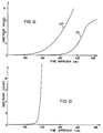
- Fig. 12 shows the flux/distance relationship for the embodiment of Fig. 11 for beam incidences of 45° and 75° (laser beams 31 and 34, respectively).
- the corresponding experimental decay lengths are 100 nm and 40 nm, respectively. It has been found that only insignificant changes in decay length occur as the angle of incidence is increased towards 90°. It is to be noted that in this figure, the abscissa has its origin in an arbitrary point where the fine approach of tip 13 towards sample 27 commences.
- a thin film of liquid metal fills the gap between tip 13 and sample 27, Fig. 11.
- the application of the metal film may, for example, be made with a pipette 35 into which some liquid metal 36 has been sucked.
- a droplet 37 of the metal can be positioned right on the spot where tip 13 approaches the surface of sample 27.
- Wetting is promoted by careful cleaning and drying, reduction of air humidity, and by thin adhesive metal coatings, such as a hue of chromium and/or gold on the sample surface and/or the tip surface.
- Fig. 13 As mentioned before, a variety of liquid metals is available for filling the gap.
- the diagram of Fig. 13 was generated with the apparatus of Fig. 11 with liquid Ga/In eutectic alloy as the gap filling, and with normal incidence of laser beam 29.
- the flux-over-distance relation yields a decay length of about 7.5 nm, which is a factor of 5 to 15 improvement over the metalless arrangement.
- the origin of the abscissa corresponds to an arbitrary point where the fine-approach was started. This point is, however, unrelated to the starting point for Fig. 12.
- the SNOM microscopy can be conducted at any angle of incidence, in particular in the normal direction which is essential for certain imaging problems.
- Scan images of the sample surface can be created with the instrument of the present invention by rastering the sample 27 with tip 13 either at constant distance or at constant flux of photons.
- Topographic and optical surface features show up in the respective other parameter of the pair, i.e., as flux or position variations.
- the lateral resolution obtained with scanning tunneling optical microscopes in general is a fraction only of the decay length, indicating that the assumption resolvable lateral details ⁇ decay length is a fairly conservative one.
- the concept of using a liquid metal as a potential barrier for tunneling photons has also other applications not directly related to microscopy.
- the concept may be applied to optical storage units where the storage medium and/or the probe tip is covered with a thin layer of liquid metal. With the resulting increase in resolving power, it will be possible to reduce the size of the individual information bits to below 10 nm, thus dramatically increasing the overall storage capacity.
- a conventional optical coupler consists of two optical fibers placed in juxtaposition, with their claddings partly removed in the region of contact.
- the coupling factor of this coupler can be made adjustable by placing a thin layer of liquid metal between the fibers in their region of contact, and by varying the thickness of the metal layer with external adjustment means, or even with the aid of the optical waves travelling along these fibers.
Landscapes
- Chemical & Material Sciences (AREA)
- Physics & Mathematics (AREA)
- Nanotechnology (AREA)
- Engineering & Computer Science (AREA)
- Optics & Photonics (AREA)
- Health & Medical Sciences (AREA)
- General Health & Medical Sciences (AREA)
- General Physics & Mathematics (AREA)
- Nuclear Medicine, Radiotherapy & Molecular Imaging (AREA)
- Radiology & Medical Imaging (AREA)
- Crystallography & Structural Chemistry (AREA)
- Analytical Chemistry (AREA)
- Life Sciences & Earth Sciences (AREA)
- Biophysics (AREA)
- Length Measuring Devices By Optical Means (AREA)
- Microscoopes, Condenser (AREA)
- Lenses (AREA)
Priority Applications (5)
| Application Number | Priority Date | Filing Date | Title |
|---|---|---|---|
| DE69223789T DE69223789T2 (de) | 1992-10-22 | 1992-10-22 | Optisches Nahfeldabtastmikroskop |
| AT92810813T ATE161636T1 (de) | 1992-10-22 | 1992-10-22 | Optisches nahfeldabtastmikroskop |
| EP92810813A EP0593835B1 (fr) | 1992-10-22 | 1992-10-22 | Microscope de balayage optique de champ proche |
| JP5207946A JP2555531B2 (ja) | 1992-10-22 | 1993-08-23 | 走査型近距離場光学顕微鏡 |
| US08/128,458 US5539197A (en) | 1992-10-22 | 1993-09-29 | Scanning near-field optical microscope having a medium denser than air in the gap between the probe chip and the sample being measured |
Applications Claiming Priority (1)
| Application Number | Priority Date | Filing Date | Title |
|---|---|---|---|
| EP92810813A EP0593835B1 (fr) | 1992-10-22 | 1992-10-22 | Microscope de balayage optique de champ proche |
Publications (2)
| Publication Number | Publication Date |
|---|---|
| EP0593835A1 true EP0593835A1 (fr) | 1994-04-27 |
| EP0593835B1 EP0593835B1 (fr) | 1997-12-29 |
Family
ID=8212010
Family Applications (1)
| Application Number | Title | Priority Date | Filing Date |
|---|---|---|---|
| EP92810813A Expired - Lifetime EP0593835B1 (fr) | 1992-10-22 | 1992-10-22 | Microscope de balayage optique de champ proche |
Country Status (5)
| Country | Link |
|---|---|
| US (1) | US5539197A (fr) |
| EP (1) | EP0593835B1 (fr) |
| JP (1) | JP2555531B2 (fr) |
| AT (1) | ATE161636T1 (fr) |
| DE (1) | DE69223789T2 (fr) |
Cited By (3)
| Publication number | Priority date | Publication date | Assignee | Title |
|---|---|---|---|---|
| WO1995033207A1 (fr) * | 1994-05-31 | 1995-12-07 | Kanagawa Academy Of Science And Technology | Fibre optique et son procede de production |
| WO1996005531A1 (fr) * | 1994-08-11 | 1996-02-22 | The Regents Of The University Of California | Procede et appareil permettant d'effectuer la microscopie optique a champ proche |
| EP0701102A1 (fr) * | 1994-09-09 | 1996-03-13 | Seiko Instruments Inc. | Microscope en champ proche à balayage/force atomique avec observation dans un fluide |
Families Citing this family (9)
| Publication number | Priority date | Publication date | Assignee | Title |
|---|---|---|---|---|
| WO1995010060A1 (fr) * | 1993-10-04 | 1995-04-13 | International Business Machines Corporation | Microscope optique en champ proche |
| US5859364A (en) * | 1995-06-05 | 1999-01-12 | Olympus Optical Co., Ltd. | Scanning probe microscope |
| US5625617A (en) * | 1995-09-06 | 1997-04-29 | Lucent Technologies Inc. | Near-field optical apparatus with a laser having a non-uniform emission face |
| US5952562A (en) * | 1995-11-22 | 1999-09-14 | Olympus Optical Co., Ltd. | Scanning probe microscope incorporating an optical microscope |
| US5796487A (en) * | 1996-06-28 | 1998-08-18 | Polaroid Corporation | Dark field, photon tunneling imaging systems and methods for optical recording and retrieval |
| DE19741122C2 (de) * | 1997-09-12 | 2003-09-25 | Forschungsverbund Berlin Ev | Anordnung zur Vermessung und Strukturierung (Nahfeldanordnung) |
| JP3416589B2 (ja) | 1999-09-14 | 2003-06-16 | 理化学研究所 | 部材の先端部に金属微粒子を生成して固定する方法およびその装置ならびにプローブ |
| US7170842B2 (en) * | 2001-02-15 | 2007-01-30 | Hewlett-Packard Development Company, L.P. | Methods for conducting current between a scanned-probe and storage medium |
| US7234343B2 (en) * | 2004-03-08 | 2007-06-26 | Virginia Tech Intellectual Properties, Inc. | Method and apparatus for evanescent filed measuring of particle-solid separation |
Citations (1)
| Publication number | Priority date | Publication date | Assignee | Title |
|---|---|---|---|---|
| US5105305A (en) * | 1991-01-10 | 1992-04-14 | At&T Bell Laboratories | Near-field scanning optical microscope using a fluorescent probe |
Family Cites Families (2)
| Publication number | Priority date | Publication date | Assignee | Title |
|---|---|---|---|---|
| EP0112401B1 (fr) * | 1982-12-27 | 1987-04-22 | International Business Machines Corporation | Microscope de balayage optique de champ proche |
| US5202004A (en) * | 1989-12-20 | 1993-04-13 | Digital Instruments, Inc. | Scanning electrochemical microscopy |
-
1992
- 1992-10-22 EP EP92810813A patent/EP0593835B1/fr not_active Expired - Lifetime
- 1992-10-22 DE DE69223789T patent/DE69223789T2/de not_active Expired - Fee Related
- 1992-10-22 AT AT92810813T patent/ATE161636T1/de not_active IP Right Cessation
-
1993
- 1993-08-23 JP JP5207946A patent/JP2555531B2/ja not_active Expired - Fee Related
- 1993-09-29 US US08/128,458 patent/US5539197A/en not_active Expired - Fee Related
Patent Citations (1)
| Publication number | Priority date | Publication date | Assignee | Title |
|---|---|---|---|---|
| US5105305A (en) * | 1991-01-10 | 1992-04-14 | At&T Bell Laboratories | Near-field scanning optical microscope using a fluorescent probe |
Non-Patent Citations (2)
| Title |
|---|
| APPLIED PHYSICS LETTERS vol. 44, no. 7, 1 April 1984, NEW YORK US pages 651 - 652 D.W.POHL ET AL. 'OPTICAL STETHOSCOPY: IMAGE RECORDING WITH RESOLUTION L/20' * |
| OPTICS COMMUNICATIONS vol. 71, no. 1/2, 1 May 1989, AMSTERDAM NL pages 23 - 28 D.COURJON ET AL. 'SCANNING TUNNELING OPTICAL MICROSCOPY' * |
Cited By (4)
| Publication number | Priority date | Publication date | Assignee | Title |
|---|---|---|---|---|
| WO1995033207A1 (fr) * | 1994-05-31 | 1995-12-07 | Kanagawa Academy Of Science And Technology | Fibre optique et son procede de production |
| WO1996005531A1 (fr) * | 1994-08-11 | 1996-02-22 | The Regents Of The University Of California | Procede et appareil permettant d'effectuer la microscopie optique a champ proche |
| EP0701102A1 (fr) * | 1994-09-09 | 1996-03-13 | Seiko Instruments Inc. | Microscope en champ proche à balayage/force atomique avec observation dans un fluide |
| US5821409A (en) * | 1994-09-09 | 1998-10-13 | Seiko Instruments Inc. | Scanning near-field optic/atomic-force microscope with observing function in liquid |
Also Published As
| Publication number | Publication date |
|---|---|
| DE69223789T2 (de) | 1998-06-25 |
| DE69223789D1 (de) | 1998-02-05 |
| US5539197A (en) | 1996-07-23 |
| ATE161636T1 (de) | 1998-01-15 |
| EP0593835B1 (fr) | 1997-12-29 |
| JPH07140155A (ja) | 1995-06-02 |
| JP2555531B2 (ja) | 1996-11-20 |
Similar Documents
| Publication | Publication Date | Title |
|---|---|---|
| EP0012262B1 (fr) | Appareil et procédé d'examen acoustique d'une partie microscopique d'un objet | |
| JP3262909B2 (ja) | 光学システム | |
| JP3095226B2 (ja) | 光子スキャニング型トンネル顕微鏡検査法 | |
| Courjon et al. | Near field microscopy and near field optics | |
| US5288996A (en) | Near-field optical microscopic examination of genetic material | |
| EP0593835B1 (fr) | Microscope de balayage optique de champ proche | |
| US5286970A (en) | Near field optical microscopic examination of a biological specimen | |
| JP4004098B2 (ja) | 走査型レーザー顕微鏡を用いた測定方法及び装置 | |
| CA1248620A (fr) | Microscope acoustique a balayage | |
| US6545276B1 (en) | Near field optical microscope | |
| Baida et al. | Combination of a fiber and a silicon nitride tip as a bifunctional detector; first results and perspectives | |
| CA2054334C (fr) | Microscope optique a balayage en champ proche et applications de ce microscope | |
| JP2000081383A (ja) | 散乱型近接場顕微鏡 | |
| JPH10170522A (ja) | 光測定装置 | |
| JPH04136743A (ja) | 光音響信号検出方法及び装置 | |
| Vuković et al. | Scanning probe microscopy (tunneling, atomic force, confocal and acoustic) in particle track detectors | |
| Sarayeddine et al. | Scanning tunneling optical microscopy (STOM) using a stylus sensor application to topography analysis of guiding surfaces | |
| Lapchuk et al. | Theoretical investigation for improvement of scanning a near-field optical microscope | |
| Thaer | Complementary and Analogous Information Obtained by Acoustic and Light Microscopy | |
| JP2004085220A (ja) | 透光孔付きカンチレバー及びその製造方法並びにそれを用いたビーム測定方法 | |
| Sulewski et al. | A description of the bell laboratories scanned acoustic microscope | |
| De Marco et al. | Development of an optical scanning tunneling microscopw | |
| Kroo | Novel optical microscopy | |
| BAIDA et al. | Université de Franche-Comté, UFR Sciences, route de Gray | |
| Ch | PO Box 6321, D-6330 Wetzlar 21 |
Legal Events
| Date | Code | Title | Description |
|---|---|---|---|
| PUAI | Public reference made under article 153(3) epc to a published international application that has entered the european phase |
Free format text: ORIGINAL CODE: 0009012 |
|
| AK | Designated contracting states |
Kind code of ref document: A1 Designated state(s): AT BE CH DE ES FR GB IT LI NL SE |
|
| 17P | Request for examination filed |
Effective date: 19940819 |
|
| 17Q | First examination report despatched |
Effective date: 19950928 |
|
| GRAG | Despatch of communication of intention to grant |
Free format text: ORIGINAL CODE: EPIDOS AGRA |
|
| GRAH | Despatch of communication of intention to grant a patent |
Free format text: ORIGINAL CODE: EPIDOS IGRA |
|
| GRAH | Despatch of communication of intention to grant a patent |
Free format text: ORIGINAL CODE: EPIDOS IGRA |
|
| GRAA | (expected) grant |
Free format text: ORIGINAL CODE: 0009210 |
|
| AK | Designated contracting states |
Kind code of ref document: B1 Designated state(s): AT BE CH DE ES FR GB IT LI NL SE |
|
| PG25 | Lapsed in a contracting state [announced via postgrant information from national office to epo] |
Ref country code: NL Free format text: LAPSE BECAUSE OF FAILURE TO SUBMIT A TRANSLATION OF THE DESCRIPTION OR TO PAY THE FEE WITHIN THE PRESCRIBED TIME-LIMIT Effective date: 19971229 Ref country code: LI Free format text: LAPSE BECAUSE OF FAILURE TO SUBMIT A TRANSLATION OF THE DESCRIPTION OR TO PAY THE FEE WITHIN THE PRESCRIBED TIME-LIMIT Effective date: 19971229 Ref country code: IT Free format text: LAPSE BECAUSE OF FAILURE TO SUBMIT A TRANSLATION OF THE DESCRIPTION OR TO PAY THE FEE WITHIN THE PRE;WARNING: LAPSES OF ITALIAN PATENTS WITH EFFECTIVE DATE BEFORE 2007 MAY HAVE OCCURRED AT ANY TIME BEFORE 2007. THE CORRECT EFFECTIVE DATE MAY BE DIFFERENT FROM THE ONE RECORDED.SCRIBED TIME-LIMIT Effective date: 19971229 Ref country code: ES Free format text: THE PATENT HAS BEEN ANNULLED BY A DECISION OF A NATIONAL AUTHORITY Effective date: 19971229 Ref country code: CH Free format text: LAPSE BECAUSE OF FAILURE TO SUBMIT A TRANSLATION OF THE DESCRIPTION OR TO PAY THE FEE WITHIN THE PRESCRIBED TIME-LIMIT Effective date: 19971229 Ref country code: BE Free format text: LAPSE BECAUSE OF FAILURE TO SUBMIT A TRANSLATION OF THE DESCRIPTION OR TO PAY THE FEE WITHIN THE PRESCRIBED TIME-LIMIT Effective date: 19971229 Ref country code: AT Free format text: LAPSE BECAUSE OF FAILURE TO SUBMIT A TRANSLATION OF THE DESCRIPTION OR TO PAY THE FEE WITHIN THE PRESCRIBED TIME-LIMIT Effective date: 19971229 |
|
| REF | Corresponds to: |
Ref document number: 161636 Country of ref document: AT Date of ref document: 19980115 Kind code of ref document: T |
|
| REG | Reference to a national code |
Ref country code: CH Ref legal event code: EP |
|
| REF | Corresponds to: |
Ref document number: 69223789 Country of ref document: DE Date of ref document: 19980205 |
|
| PG25 | Lapsed in a contracting state [announced via postgrant information from national office to epo] |
Ref country code: SE Free format text: LAPSE BECAUSE OF FAILURE TO SUBMIT A TRANSLATION OF THE DESCRIPTION OR TO PAY THE FEE WITHIN THE PRESCRIBED TIME-LIMIT Effective date: 19980329 |
|
| ET | Fr: translation filed | ||
| NLV1 | Nl: lapsed or annulled due to failure to fulfill the requirements of art. 29p and 29m of the patents act | ||
| REG | Reference to a national code |
Ref country code: CH Ref legal event code: PL |
|
| PLBE | No opposition filed within time limit |
Free format text: ORIGINAL CODE: 0009261 |
|
| 26N | No opposition filed | ||
| PGFP | Annual fee paid to national office [announced via postgrant information from national office to epo] |
Ref country code: FR Payment date: 19991018 Year of fee payment: 8 |
|
| PG25 | Lapsed in a contracting state [announced via postgrant information from national office to epo] |
Ref country code: FR Free format text: LAPSE BECAUSE OF NON-PAYMENT OF DUE FEES Effective date: 20010629 |
|
| REG | Reference to a national code |
Ref country code: FR Ref legal event code: ST |
|
| REG | Reference to a national code |
Ref country code: GB Ref legal event code: IF02 |
|
| PGFP | Annual fee paid to national office [announced via postgrant information from national office to epo] |
Ref country code: DE Payment date: 20031017 Year of fee payment: 12 |
|
| PG25 | Lapsed in a contracting state [announced via postgrant information from national office to epo] |
Ref country code: DE Free format text: LAPSE BECAUSE OF NON-PAYMENT OF DUE FEES Effective date: 20050503 |
|
| REG | Reference to a national code |
Ref country code: GB Ref legal event code: 746 Effective date: 20080925 |
|
| PGFP | Annual fee paid to national office [announced via postgrant information from national office to epo] |
Ref country code: GB Payment date: 20101022 Year of fee payment: 19 |
|
| REG | Reference to a national code |
Ref country code: GB Ref legal event code: PE20 Expiry date: 20121021 |
|
| PG25 | Lapsed in a contracting state [announced via postgrant information from national office to epo] |
Ref country code: GB Free format text: LAPSE BECAUSE OF EXPIRATION OF PROTECTION Effective date: 20121021 |