EP0593918A1 - Kommunikationssteuerungsanlage - Google Patents
Kommunikationssteuerungsanlage Download PDFInfo
- Publication number
- EP0593918A1 EP0593918A1 EP93115188A EP93115188A EP0593918A1 EP 0593918 A1 EP0593918 A1 EP 0593918A1 EP 93115188 A EP93115188 A EP 93115188A EP 93115188 A EP93115188 A EP 93115188A EP 0593918 A1 EP0593918 A1 EP 0593918A1
- Authority
- EP
- European Patent Office
- Prior art keywords
- data
- reply
- functioning
- transmitting
- data line
- Prior art date
- Legal status (The legal status is an assumption and is not a legal conclusion. Google has not performed a legal analysis and makes no representation as to the accuracy of the status listed.)
- Granted
Links
Images










Classifications
-
- H—ELECTRICITY
- H04—ELECTRIC COMMUNICATION TECHNIQUE
- H04L—TRANSMISSION OF DIGITAL INFORMATION, e.g. TELEGRAPHIC COMMUNICATION
- H04L12/00—Data switching networks
- H04L12/28—Data switching networks characterised by path configuration, e.g. LAN [Local Area Networks] or WAN [Wide Area Networks]
- H04L12/40—Bus networks
- H04L12/40006—Architecture of a communication node
- H04L12/40013—Details regarding a bus controller
-
- H—ELECTRICITY
- H04—ELECTRIC COMMUNICATION TECHNIQUE
- H04L—TRANSMISSION OF DIGITAL INFORMATION, e.g. TELEGRAPHIC COMMUNICATION
- H04L12/00—Data switching networks
- H04L12/02—Details
- H04L12/16—Arrangements for providing special services to substations
- H04L12/18—Arrangements for providing special services to substations for broadcast or conference, e.g. multicast
- H04L12/1863—Arrangements for providing special services to substations for broadcast or conference, e.g. multicast comprising mechanisms for improved reliability, e.g. status reports
- H04L12/1877—Measures taken prior to transmission
-
- H—ELECTRICITY
- H04—ELECTRIC COMMUNICATION TECHNIQUE
- H04L—TRANSMISSION OF DIGITAL INFORMATION, e.g. TELEGRAPHIC COMMUNICATION
- H04L12/00—Data switching networks
- H04L12/28—Data switching networks characterised by path configuration, e.g. LAN [Local Area Networks] or WAN [Wide Area Networks]
- H04L12/40—Bus networks
- H04L12/407—Bus networks with decentralised control
- H04L12/413—Bus networks with decentralised control with random access, e.g. carrier-sense multiple-access with collision detection [CSMA-CD]
-
- H—ELECTRICITY
- H04—ELECTRIC COMMUNICATION TECHNIQUE
- H04L—TRANSMISSION OF DIGITAL INFORMATION, e.g. TELEGRAPHIC COMMUNICATION
- H04L12/00—Data switching networks
- H04L12/28—Data switching networks characterised by path configuration, e.g. LAN [Local Area Networks] or WAN [Wide Area Networks]
- H04L12/40—Bus networks
- H04L12/40006—Architecture of a communication node
- H04L12/40032—Details regarding a bus interface enhancer
Definitions
- the present invention relates to a communication control apparatus which controls data communication, and particularly, to a communication control apparatus by a CSMA/CD (carrier Sense Multiple Access with Collision Detection) method which is one accessing method of a LAN (Local Area Network).
- CSMA/CD carrier Sense Multiple Access with Collision Detection
- a CSMA/CD method is frequently used as an accessing method.
- a communication system by a conventional communication control apparatus adopting the CSMA/CD method is described with reference to Fig. 1 and Fig. 2.
- Fig. 1 is a schematic view showing an example of connection between the conventional communication apparatuses 2, 3, 4 and 5 (hereinafter referred to as A, B, C and D units) each having a bus contention control function by the CSMA/CD accessing method, and a common data line 1.
- the units 2, 3, 4 and 5 are respectively connected to the common data line 1 through transmitting lines designated by reference numerals 6, 8, 10 and 12, and receiving lines designated by the reference numerals 7, 9, 11 and 13 in the figure, constituting a communication system.
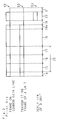
- FIG. 2 An example of a communication format used in such a communication system is shown in a schematic view of Fig. 2.
- the communication format shown in Fig. 2 is a format published by the U. S. Automobile Engineering Association as SAE-J1850.
- This communication format is constituted by, a transmit start mark 14 which transfers a transmit start to all of the units connected to the common data line 1, a priority code 15 which decides priority at the time of collision in a bus contention control method, destination address 16 showing a transmitting destination, a source address 17 showing a transmitting source, a communication data area 18, an error detection code (hereinafter, referred to as a CRC) 18b showing the CRC operation result from the first bit of the priority code 15 to a final bit of the communication data area 18, an area (hereinafter, referred to as an EOD) 19 showing completion of communication data, an area (hereinafter, referred to as an IFR) 20 which is replied to a transmitting unit when normally received at a receiving unit, and an area (hereinafter, referred to as an EOF) 21 showing completion of a communication frame.
- the priority code 15, destination address 16 and source address 17 are generally called a communication control area 22.
- Inherent addresses (hereinafter, referred to as the source address) are allocated respectively to the units 2, 3, 4 and 5 connected to the common data line 1.
- the source address the destination address 16 in the transmitting frame 50 sent by the A unit 2 becomes the source address of the D unit 5.
- the D unit 5 conducts receiving processing when the destination address 16 in a frame 49 on the common data line 1 coincides with the source address allocated to itself.
- the source address 17 in the transmitting frame 50 sent by the A unit 2 becomes the source address allocated to the A unit 2.
- the A unit 2 informs to the D unit 5 that the transmitting source of the transmitting frame 49 on the common data line 1 is the A unit 2 itself.
- the frame 49 as shown in Fig. 2 is sent to the common data line 1.
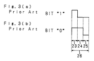
- a bit format in which a signal representing bits of "1" or "0" constituting the aforementioned communication format is subjected to pulse width modulation (hereinafter, referred to as a PWM), is described with reference to a wave-form diagram of Fig. 3.
- PWM pulse width modulation
- An area 26 of each one bit is constituted by a first time 23, a second time 24 and a third time 25.
- the bit "1" is so represented that, the first time 23 is high level (hereinafter, referred to as "H"), and the second time 24 and the third time 25 are low level (hereinafter, referred to as "L").
- the bit "0” is so represented that, as shown in Fig. 3(b), the first time 23 and the second tie 24 are given at "H” and the third time 25 is "L".
- a timing chart of the communication when the A unit 2 obtains the priority and sends the transmitting frame 50 as shown in Fig. 4(b) is shown.
- the C unit 4 replies the IFR 20 as the reply IFR 52 as shown in Fig. 4(d), this is because that the destination address 16 in the transmitting frame 50 of the A unit 2 coincides with the source address of the C unit 4, and the C unit 4 moves to the receiving processing and detects the normal receiving.
- the A unit 2 sends out a "00(H)" (here, (H) indicates a hexadecimal) 62 to the common data line 1 having the specification as stated above, as the priority code 15 as shown in Fig. 5(b), and the B unit 2 sends out a "0F(H)” 63 as shown in Fig. 5(c).
- the collision occurs at a fifth bit of the priority code 15 sent out respectively by the A unit 2 and the B unit 3.
- the wave form having longer "H” level, or the "H” level of the fifth bit of the wave form 62 outputted from the A unit 2 shown in Fig. 5(b) appears on the common data line 1, as a wave form 61 of the priority code 15 as shown in Fig. 5(a).
- the B unit 3 detects that the wave form 63 of "0F(H)" outputted by itself does not appear on the common data line 1, by comparing a wave form inputted to itself from the common data line 1 via the receiving line 9, with a wave form outputted to the common data line 1 by itself (hereinafter, referred to as an echo back comparison) to detect the collisions, and stops to send out the transmitting frame 51 thereafter as shown in Fig. 4(c).
- the bus contention control is realized in the above-mentioned manner.
- a multiple address communication As one of the communication system using the bus contention control as described above, there is a communication method called a multiple address communication.
- the multiple address communication is described according to a timing chart of the communication example shown in Fig. 6.
- a multiple address communication code decided in the communication system in advance is outputted.
- the "FF(H)" becomes the multiple address communication code.
- the B unit 3, C unit 4 and D unit 5 connected to the common data line 1 move to the receiving processing (hereinafter, referred to as a multiple address receiving) at the time point when it is detected that the destination address of the transmitting frame 50 outputted from the A unit 2 to the common data line 1 is the "FF(H)".
- the B unit 3, C unit 4 and D unit 5 thus moved to the multiple address receiving processing never reply the IFR 20 as shown in Fig. 6(a) regardless of occurrence of the receiving errors, ever, when the EOD 19 indicating the completion of communication data of the transmitting frame is detected. This is because, even when a plurality of receiving units reply the IFR 20 simultaneously, they collide with each other on the common data line 1, so that they are meaningless for the transmitting unit of the receiving side.
- the multiple address communication takes place as mentioned above, so that the transmitting unit could not find out the occurrence of errors on the receiving unit side within one message frame.
- the present invention has been devised to solve such problems as described above, therefore, it is an object thereof to provide a communication control apparatus capable of finding occurrence of errors in a unit on the receiving side in a unit on the transmitting side by one frame communication, improving accuracy of multiple address communication and easily retrieving the source address of the unit having an unspecific source address in one specific unit.
- the communication control apparatus is constituted such that, when functioning as a receiving side, a replay data row is replied only when receiving normally or only when not receiving normally.
- the communication control apparatus is also constituted such that, even at the time of multiple address communication, when functioning as the receiving side, the replay data row is replied only when receiving normally, or only when not receiving normally.
- the communication control apparatus of the present invention is constituted such that, at the time of multiple address communication, the reply data row is replied only when a predetermined code sent from the transmitting side is larger than respective source addresses, or only when smaller.
- the reply data row is replied on the receiving side when receiving normally or not receiving normally, on the transmitting side, it is possible to find whether or not the receiving side has received normally within one frame.
- the communication control apparatus of the present invention at the time of multiple address communication, by constituting such that all of the communication terminals receiving normally reply the reply data row, it is possible to find within one frame that, at least, one communication terminal has received normally when the replay data row is detected on the transmitting side, and when the reply data row is not detected, it is possible to find that all the communication terminals could not receive normally.
- the communication control apparatus of the present invention since it is constituted such that, only the communication terminal having the source address larger than a code sent from the transmitting side replies the source address as the reply data row, the number of communication terminals connected to the common data line and the source addresses of the respective communication terminals can be retrieved.
- the communication control apparatus of the present invention since it is constituted such that, only the communication terminal having the source address smaller than the code sent from the transmitting side replies the source address as the reply data row, the number of communication terminals connected to the common data line and the source addresses of the respective communication terminals can be retrieved.
- Fig. 7 is a block diagram showing an example of configuration of transmitting and receiving units of a communication control apparatus of the present invention.
- the communication control apparatus of the present invention is designated by reference numeral 27, and is constituted by a transmitting unit 27T, a receiving unit 27R, source address registers 28, a sequence control unit 44, a reply IFR register 42, an echo back comparison detecting unit 43 and so on.
- the transmitting unit 27T is connected to a common data line 1 through a transmitting line 6, and the receiving unit 27R is connected to the same through a receiving line 7.
- a microcomputer is connected to the communication control apparatus 27 of the present invention at the left side in Fig. 7.
- source addresses allocated to the communication control apparatus 27 are inputted from the external microcomputer via a signal line 45.
- the sequence control unit 44 is controlled by a control signal given from the microcomputer via a signal line 47.
- the echo back comparison detecting unit 43 compares the echo backs as to be described later.
- the replay IFR register 42 stores a reply IFR given from the receiving unit 27R.
- the transmitting unit 27T is constituted by a transmitting buffer memory 29, a selector 30, a P to S (Parallel to Serial) shift register 31, a PWM (Pulse Width Modulation) unit 32, a selector 33, a transmit start mark generating unit 34, a transmitting buffer 35 and so on.
- the transmitting buffer memory 29 stores temporarily a data row to be sent which is given from the external microcomputer via a signal line 46.
- the data row stored in the transmitting buffer memory 29 is given to the selector 30 as parallel data via a signal line 81.
- the source address stored in the source address register 28 is also given to the selector 30 via a signal line 82, and either of the source address or the data row is selected by the control signal given from the sequence control unit 44 via signal lines 83, 84, and inputted to the P to S shift register 31.
- the P to S shift register 31 converts the parallel data inputted from the aforesaid selector 30 via signal line 85 into serial data, which is outputted to the PWM unit 32 and the echo back comparison detecting unit 43 via a signal line 86.
- the PWM unit 32 outputs the serial data outputted from the P to S shift register 31 to the selector 33 via a signal line 87 after the pulse width modulation.
- the transmit start mark generating unit 34 generates a transmit start mark according to a control signal given from the sequence control unit 44 via a signal line 88, and outputs it to the aforesaid selector 33 via a signal line 89.
- the selector 33 selects either a bit pattern after PWM modulated to be outputted to the signal line 87 from the PWM unit 32, or the transmit start mark to be outputted from the transmit start mark generating unit 34 to the signal line 89, and outputs it to the transmitting line 6 via the output buffer 35.
- the receiving unit 27R is constituted by a receiving buffer 36, a digital filter 37, a PWDM (Pulse Width Demodulation) unit 38, a receiving error detecting unit 39, an S to P (Serial to Parallel) shift register 40, a receiving buffer memory 41 and so on.
- PWDM Pulse Width Demodulation
- the receiving buffer 36 inputs a signal from the common data line 1 via the receiving line 7 and gives it to the digital filter 37.
- the digital filter 37 removes noise components from the inputted signal, and gives it to the PWDM unit 38 and the receiving error detecting unit 39 via a signal line 91.
- the PWDM Unit 38 gives the signal given from the digital filter 37 to the echo back comparison detecting unit 43, S to P shift register 40 and receiving error detecting unit 39 via a signal line 92 after pulse width demodulated.
- the S to P shift register 40 converts serial data into parallel data to write data outputted from the PWDM unit 38 into the receiving buffer memory 41 via a signal line 93.
- a control signal which operates the S to P shift register 40 is inputted from the sequence control unit 44 via a signal line 94 when destination address data in the receiving frame and source address data stored in the source address register 28 are coincided after being compared, or when data signifying the multiple address communication and the destination address data are coincided after being compared.
- a control signal showing a section, wherein the reply IFR is to be stored is given from the sequence control unit 44 via a signal line 95, and a data output line 96 is connected from the S to P shift register 40.
- an output of the PWDM unit 38 and an output of the P to S shift register 31 are connected, and moreover, a comparison timing control signal is given from the sequence control unit 44 via a signal lie 97.
- Output of the comparison results by the echo back comparison detecting unit 43 is inputted to the sequence control unit 44 via signal line 98.
- the sequence control unit 44 outputs the control signal stopping its operation to the P to S shift register 31 via the signal line 84 and stops transmission of the transmitting frame.
- the communication control apparatus 27 of the present invention shown in Fig. 7 corresponds respectively to the units 2, 3, 4 and 5 shown in Fig. 1.
- the A unit 2 sends out a transmitting frame 50 to the common data line 1.
- the sequence control unit 44 respectively detects that the destination address 16 in the transmitting frame 50 sent to the common data line 1 from the A unit 2 is the "FF(H)" to start the P to S shift register 40 to operate, and moves to the receiving processing.
- the source addresses of the B unit 3, C unit 4 and D unit 5 are respectively set to "07(H)", “3F(H)” and "0F(H)” in order as shown in Figs. 8(c), (d) and (e).
- a control signal showing an IFR reply section is inputted to the selector 30 from the sequence control unit 44.
- the contents of the source address register 28 are inputted.
- the echo back comparison for the IFR 20 sent by each of the units 3, 4 and 5 itself is performed in each of the units 3, 4 and 5.
- the IFR 20 replied from the units 3, 4 and 5 is subjected to the echo back comparison with the IFR 20 of the frame 49 on the common data line 1 in the respective echo back comparison detecting units 43.
- the units 3, 4 and 5 it is detected that wave forms of the IFR 20 respectively outputted do not appear on the IFR 20 of the frame 49 on the common data line 1 shown in Fig. 8(a), by comparing the wave form inputted from the receiving line 9 and the wave form outputted by each of the units 3, 4 and 5 itself in the echo back comparison detecting unit 43, and stops to send the IFR 20 thereafter.
- the C unit 4 among the B, C, D units 3, 4, 5 which start replying the IFR 20 at the same time detects that a bit wave form 52 of the IFR 20 sent by itself differs from a bit wave form 54 shown in Fig. 9(a) inputted from the common data line 1 via the receiving buffer 36 at a third bit, and stops to reply the IFR 20. Also, as shown in Fig.
- the D unit 5 detects that, a bit wave form 53 of the IFR 20 sent by itself differs from the bit wave form 54 shown in Fig. 9(a) inputted from the common data line 1 via the receiving buffer 36 at a fifth bit, and similarly stops to reply the IFR 20. And, as shown in Fig. 9(b), only the IFR 20 of "07(H)" replied by the B unit 3 is replied to the A unit 2 which is the transmitting unit.
- the A unit 2 can detect within a period of one frame, that, at least, the B unit 3 among the B, C, D units 3, 4 and 5 connected to the common data line 1, has received normally the transmitting frame sent from the A unit 2.
- the A unit 2 can find out that all the other receiving units 3, 4 and 5 except itself, which are connected to the common data line 1, have received normally, when the IFR is not replied at all.
- the A unit 20 can find out that the receiving error occurs, at least, in the receiving unit which has replied the IFR unit 20.
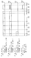
- Fig. 10 is a timing chart showing a state of communication frame according to the second invention.
- the A unit 2 sends out the transmitting frame 50 to the common data line 1.
- an IFR control code 57 is set between the source address 17 and a communication data area 18.
- the A unit 2 is to output "10(H)" as the IFR control code 57.
- the destination address 16 in the frame 50 sent on the common data line 1 from the A unit 2 is a multiple address communication code "FE(H)" signifying the multiple address communication, respective P to S shift registers 40 start to operate and move to the receiving processing.
- the IFR control code 57 in the frame on the common data line 1 is inputted from the common data line 1 via the receiving buffer 36, and data of the IFR control code 57 are stored in the reply IFR register 42.
- Fig. 11 is a circuit diagram showing an example of configuration of a circuit for comparing the IFR control code 57 stored in the aforesaid reply IFR register 42 and the source address stored in the source address register 28, or an IFR control circuit.
- the IFR control circuit is provided inside of the sequence control unit 14.
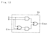
- reference numerals 55a to 55h designate logic circuits having the same configuration and constituted by the logic circuit having the circuit configuration designated by reference numeral 55 in Fig. 12.
- Respective bits of the output signal of the source address register 28 of 8-bit configuration are inputted to input terminals A of the logic circuits 55a to 55h, and similarly, respective bits of the output signal of the reply IFR register 42 of 8-bit configuration are respectively inputted to input terminals B of the logic circuits 55a to 55h via inverters 72.
- Output terminals Cout of the logic circuits 55a to 55h are respectively connected to input terminals Cin of the logic circuits 55b to 55h in the next stage, and only the input terminal Cin of the logic circuit 55a in the first stage is fixed at "L" level.
- a C output 56 from the output terminal Cout of the logic circuit 55h in the last stage turns into the "L” level when VA ⁇ VB, and turn into "H” level when VA > VB when it is assumed that a value held by the source address register 28 is VA and a value held by the reply IFR register 42 is VB.
- the units 3, 4 and 5 on the receiving side compare respective source address data with data of the IFR control code 57 outputted from the A unit 2 to judge mathematical differences. After detecting EOD indicating the completion of the frame, the receiving side units 3, 4 and 5 reply the IFR 20.
- the unit shown in Fig. 11 whose C output 56 of the IFR control circuit is at "H" level, that is, the D unit outputs the control signal from the sequence control unit 44 and stops the operation of the P to S shift register 31, thereby, does not reply the IFR 20 as shown in Fig. 13(d). And, as shown in Figs.
- the IFR control circuit shown in Fig. 11 operates similarly as above-mentioned case, and only in, the D unit 5 whose source address is set to "F0(H)", the C output 56 of the IFR control circuit becomes "H" level.
- the D unit 5 since it is so set that only the unit which becomes "H” level replies the IFR to the sequence control unit 44, as shown in Fig. 14(e) and Fig. 15(d), only the D unit 5 replies the IFR 20, and the B unit 3 and C unit 4 each of whose C output 56 of the IFR control circuit has become "L" level do not reply the IFR 20 as shown in Figs. 14(c), (d) and Figs. 15 (b), (c). That is, the IFR 20 of the D unit 5 is replied to the A unit 2 on the transmitting side as shown in Fig. 14(a) and Fig. 15 (a).
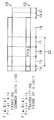
- the A unit 2 sets the destination address 16 to "FF(H)" and sends the transmitting frame 50 to the common data line 1.
- the B, C and D units 3, 4 and 5 all conduct receiving processing to the transmitting frame 50, and reply the IFR 20 after detecting the EOD 19.
- the C, D units 4, 5 detect a collision in the IFR reply section and stop to reply the IFR 20.
- the source address "05(H)" of the B unit 3 is replied to the A unit 2 on the transmitting side as the IFR 20.
- the A unit 2 sets the destination address to "FE(H)" and the IFR control code to "05(H)" of the B unit 3, which is the smallest source address detected previously, and sends the transmitting frame to the common data line 1.
- the B, C and D units 3, 4 and 5 all conduct receiving processing for the frame sent by the A unit 2.
- the B, C and D units 3, 4 and 5 compare "05(H)", the value of the IFR control code with the source addresses set in itself, arid after the C unit 4 and D unit 5 set to the mathematically larger source addresses detect the EOD respectively, reply the IFR 20 shown in Figs. 18(d), (e).
- the D unit 5 detects a collision in the IFR reply section, and stops to reply the IFR 20.
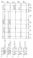
- the source address "15(H)" of the C unit 4 is replied to the A unit 2 on the transmitting side as the IFR 20 as shown in Fig. 18(a).
- the A unit 2 finds out that, the source address among those set in the units connected to the communication system, which is mathematically smaller than "05(H)", is "15(H)".
- the A unit 2 sets the destination address to "FE(H)" and the IFR control code to "15(H)" of the C unit 4, which is the next smallest source address detected previously, and sends the transmitting frame.
- the B, C and D units 3, 4 and 5 all conduct receiving processing.
- the B, C and D units 3, 4 and 5 compare "15(H)", the value of the IFR control code 57 with the source addresses set to itself.
- the value of the IFR control code 57 detects the EOD, replies the IFR 20 shown in Fig. 19(e).
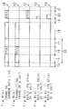
- the A unit 2 By receiving "5A(H)", the value of the IFR 20 in the frame 49 on the common data line 1 shown in Fig. 19(a), the A unit 2 finds out that, the next mathematically smaller source address among those set in the units connected to the communication system is "5A(H)".
- the A unit 2 sets the destination address to "FE(H)" and the IFR control code to "5A(H)" of the D unit 5, which is the next smaller source address detected previously, and sends out the transmitting frame.
- the B, C and D units 3, 4 arid 5 all conduct receiving processing.
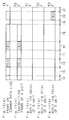
- the B, C and D units 3, 4 and 5 compare the value "5A(H)" of the IFR control code 57 and the source addresses set in itself. As the result, since there is no unit to which the source address, which is mathematically larger than "5A(H)", the value of the IFR control code 57 is set, as shown in Figs.
- respective source addresses and the number of units connected to the common data line 1 are retrieved, by replying the IFR 20 by the unit to which the source address which is mathematically larger than the IFR control code 57 is set.
- the similar effect may be obtained by the configuration, in which the unit to which the source address which is mathematically smaller than the IFR control code 57 is set, replies the IFR 20.
- Whether to reply the IFR 20 by the unit to which the source address which is larger than the IFR control code 57 is set, or to reply the IFR 20 by the unit to which the source address which is smaller than the IFR control code 57 is set, may be controlled by data included in the frame sent to the common data line 1 from the unit on the transmitting side.
- whether to replay the IFR 20 from the unit wherein the receiving error is produced, or to reply the IFR 20 from the unit wherein the receiving error is not produced, or to send the IFR 20 in any case, may be controlled by data included in the frame.
- the communication control apparatus of the present invention it is possible to find out on the transmitting side whether or not receiving side has received normally, by one frame communication.
- the communication control apparatus of the present invention at the time of multiple address communication, when it is constituted such that, the IFR is replied by the unit wherein the receiving error is not produced, it can be found out that, at least, one communication terminal has received normally on the transmitting side, and when the IFR is not replied at all, it can be found out that all of the communication terminals have not received normally.
- the communication control apparatus of the present invention at the time of multiple address communication, when it is constituted such that, the IFR is replied by the unit wherein the receiving error is produced, it can be found out that, at least, one communication terminal produces the communication error on the transmitting side, and when the IFR is not replied at all, it can be found out that all of the communication terminals have received normally.
- the communication control apparatus of the present invention at the time of multiple address communication using the IFR control code, since the IFR is replied only by the unit having the source address which is mathematically larger than the IFR control code, or the unit having the source address which is mathematically smaller, when the multiple address communication is repeated while changing the IFR control code sequentially, respective source addresses and the number of communication terminals connected to the common data line can be retrieved.
Landscapes
- Engineering & Computer Science (AREA)
- Computer Networks & Wireless Communication (AREA)
- Signal Processing (AREA)
- Small-Scale Networks (AREA)
Applications Claiming Priority (2)
| Application Number | Priority Date | Filing Date | Title |
|---|---|---|---|
| JP281663/92 | 1992-10-20 | ||
| JP4281663A JP2844036B2 (ja) | 1992-10-20 | 1992-10-20 | 通信制御装置 |
Publications (2)
| Publication Number | Publication Date |
|---|---|
| EP0593918A1 true EP0593918A1 (de) | 1994-04-27 |
| EP0593918B1 EP0593918B1 (de) | 1999-02-17 |
Family
ID=17642247
Family Applications (1)
| Application Number | Title | Priority Date | Filing Date |
|---|---|---|---|
| EP93115188A Expired - Lifetime EP0593918B1 (de) | 1992-10-20 | 1993-09-21 | Kommunikationsendgerät |
Country Status (4)
| Country | Link |
|---|---|
| US (1) | US5384778A (de) |
| EP (1) | EP0593918B1 (de) |
| JP (1) | JP2844036B2 (de) |
| DE (1) | DE69323521T2 (de) |
Families Citing this family (3)
| Publication number | Priority date | Publication date | Assignee | Title |
|---|---|---|---|---|
| JP3251531B2 (ja) * | 1997-06-19 | 2002-01-28 | 矢崎総業株式会社 | 障害検出方法及び通信システム |
| WO2000004701A1 (en) * | 1998-07-16 | 2000-01-27 | Intervoice Limited Partnership | System and method for managing prepaid wireless service |
| DE102010023569A1 (de) * | 2010-06-08 | 2011-12-08 | Siemens Aktiengesellschaft | Verteiltes Kommunikationssystem, insbesondere für Leistungsschalter |
Citations (4)
| Publication number | Priority date | Publication date | Assignee | Title |
|---|---|---|---|---|
| JPS6059847A (ja) * | 1983-09-12 | 1985-04-06 | Nippon Telegr & Teleph Corp <Ntt> | 同報通信確認方式 |
| EP0241018A2 (de) * | 1986-04-11 | 1987-10-14 | Hitachi, Ltd. | Verfahren zur Mehradresskommunikation |
| EP0319271A2 (de) * | 1987-11-30 | 1989-06-07 | The Furukawa Electric Co., Ltd. | Multiplex-Übertragungssystem |
| EP0367177A2 (de) * | 1988-10-31 | 1990-05-09 | The Furukawa Electric Co., Ltd. | Multiplex-Übertragungssystem für Kraftfahrzeuge |
Family Cites Families (6)
| Publication number | Priority date | Publication date | Assignee | Title |
|---|---|---|---|---|
| US4715031A (en) * | 1985-09-23 | 1987-12-22 | Ford Motor Company | Vehicular data transfer communication system |
| JPH01289339A (ja) * | 1988-05-17 | 1989-11-21 | Mitsubishi Electric Corp | 通信制御装置 |
| JP2904283B2 (ja) * | 1989-05-22 | 1999-06-14 | マツダ株式会社 | 車両用多重伝送装置 |
| JPH0693686B2 (ja) * | 1989-07-31 | 1994-11-16 | 松下電器産業株式会社 | アドレス自動設定方式 |
| JPH0824298B2 (ja) * | 1990-02-08 | 1996-03-06 | 日本電気株式会社 | Csma方式通信システム |
| JP2904298B2 (ja) * | 1990-03-30 | 1999-06-14 | マツダ株式会社 | 車両用多重伝送装置 |
-
1992
- 1992-10-20 JP JP4281663A patent/JP2844036B2/ja not_active Expired - Fee Related
-
1993
- 1993-09-21 DE DE69323521T patent/DE69323521T2/de not_active Expired - Fee Related
- 1993-09-21 EP EP93115188A patent/EP0593918B1/de not_active Expired - Lifetime
- 1993-10-01 US US08/130,254 patent/US5384778A/en not_active Expired - Lifetime
Patent Citations (4)
| Publication number | Priority date | Publication date | Assignee | Title |
|---|---|---|---|---|
| JPS6059847A (ja) * | 1983-09-12 | 1985-04-06 | Nippon Telegr & Teleph Corp <Ntt> | 同報通信確認方式 |
| EP0241018A2 (de) * | 1986-04-11 | 1987-10-14 | Hitachi, Ltd. | Verfahren zur Mehradresskommunikation |
| EP0319271A2 (de) * | 1987-11-30 | 1989-06-07 | The Furukawa Electric Co., Ltd. | Multiplex-Übertragungssystem |
| EP0367177A2 (de) * | 1988-10-31 | 1990-05-09 | The Furukawa Electric Co., Ltd. | Multiplex-Übertragungssystem für Kraftfahrzeuge |
Non-Patent Citations (1)
| Title |
|---|
| PATENT ABSTRACTS OF JAPAN vol. 009, no. 193 (E - 334) 9 August 1985 (1985-08-09) * |
Also Published As
| Publication number | Publication date |
|---|---|
| JPH06132961A (ja) | 1994-05-13 |
| DE69323521T2 (de) | 1999-07-08 |
| DE69323521D1 (de) | 1999-03-25 |
| US5384778A (en) | 1995-01-24 |
| EP0593918B1 (de) | 1999-02-17 |
| JP2844036B2 (ja) | 1999-01-06 |
Similar Documents
| Publication | Publication Date | Title |
|---|---|---|
| CA1283228C (en) | Multiplex transmission system | |
| JP3115322B2 (ja) | メッセージの形成方法 | |
| US5430843A (en) | Data transmission system and method for transmitting data having real-time and non-real-time characteristics | |
| US4558428A (en) | Data transmission system adapted to facilitate detection of safe receipt of a transmitted data frame by a receiving station | |
| US6901469B2 (en) | Communication control apparatus using CAN protocol | |
| EP0831621B1 (de) | Kommunikationssteuerungsanlage | |
| EP0621709A1 (de) | Nachrichtenübertragungssystem | |
| EP0866401B1 (de) | Informationsidentifikationssystem zur Antwortgeberidentifizierung | |
| EP0593918B1 (de) | Kommunikationsendgerät | |
| EP0830766B1 (de) | Digitales datenbussystem mit arbitrierung | |
| US20040160976A1 (en) | Communication apparatus and method for supporting carrier sense multiple access/collision detection | |
| US5003556A (en) | Squelch circuit | |
| US4852091A (en) | High capacity communication system utilizing OR-type channels | |
| US4899143A (en) | High capacity communication system over collision-type channels | |
| US6026094A (en) | Digital data bus system including arbitration | |
| JPH0457140B2 (de) | ||
| JP3207670B2 (ja) | 通信方法 | |
| JP3042822B2 (ja) | バス競合制御方式 | |
| JPS6165552A (ja) | 通信方式 | |
| JPH04123628A (ja) | Csma/cd方式ノードステーション | |
| JPS5987528A (ja) | 連結デ−タの保証方式 | |
| JPS63314038A (ja) | マルチアクセスプロトコルの方法 | |
| JPS6366462B2 (de) | ||
| JPH03106143A (ja) | データ通信システムの通信異常検査方法 | |
| JPS63164549A (ja) | バス型ネツトワ−ク通信装置の呼出し検出方式 |
Legal Events
| Date | Code | Title | Description |
|---|---|---|---|
| PUAI | Public reference made under article 153(3) epc to a published international application that has entered the european phase |
Free format text: ORIGINAL CODE: 0009012 |
|
| AK | Designated contracting states |
Kind code of ref document: A1 Designated state(s): DE FR GB |
|
| 17P | Request for examination filed |
Effective date: 19940309 |
|
| 17Q | First examination report despatched |
Effective date: 19970506 |
|
| GRAG | Despatch of communication of intention to grant |
Free format text: ORIGINAL CODE: EPIDOS AGRA |
|
| GRAG | Despatch of communication of intention to grant |
Free format text: ORIGINAL CODE: EPIDOS AGRA |
|
| GRAH | Despatch of communication of intention to grant a patent |
Free format text: ORIGINAL CODE: EPIDOS IGRA |
|
| GRAH | Despatch of communication of intention to grant a patent |
Free format text: ORIGINAL CODE: EPIDOS IGRA |
|
| GRAA | (expected) grant |
Free format text: ORIGINAL CODE: 0009210 |
|
| AK | Designated contracting states |
Kind code of ref document: B1 Designated state(s): DE FR GB |
|
| ET | Fr: translation filed | ||
| REF | Corresponds to: |
Ref document number: 69323521 Country of ref document: DE Date of ref document: 19990325 |
|
| PLBE | No opposition filed within time limit |
Free format text: ORIGINAL CODE: 0009261 |
|
| 26N | No opposition filed | ||
| REG | Reference to a national code |
Ref country code: GB Ref legal event code: IF02 |
|
| PGFP | Annual fee paid to national office [announced via postgrant information from national office to epo] |
Ref country code: FR Payment date: 20060908 Year of fee payment: 14 |
|
| PGFP | Annual fee paid to national office [announced via postgrant information from national office to epo] |
Ref country code: DE Payment date: 20060914 Year of fee payment: 14 |
|
| PGFP | Annual fee paid to national office [announced via postgrant information from national office to epo] |
Ref country code: GB Payment date: 20060920 Year of fee payment: 14 |
|
| GBPC | Gb: european patent ceased through non-payment of renewal fee |
Effective date: 20070921 |
|
| PG25 | Lapsed in a contracting state [announced via postgrant information from national office to epo] |
Ref country code: DE Free format text: LAPSE BECAUSE OF NON-PAYMENT OF DUE FEES Effective date: 20080401 |
|
| REG | Reference to a national code |
Ref country code: FR Ref legal event code: ST Effective date: 20080531 |
|
| PG25 | Lapsed in a contracting state [announced via postgrant information from national office to epo] |
Ref country code: FR Free format text: LAPSE BECAUSE OF NON-PAYMENT OF DUE FEES Effective date: 20071001 |
|
| PG25 | Lapsed in a contracting state [announced via postgrant information from national office to epo] |
Ref country code: GB Free format text: LAPSE BECAUSE OF NON-PAYMENT OF DUE FEES Effective date: 20070921 |