EP0593924A1 - Dispositif pour la production d'un plasma au moyen d'une pulvérisation cathodique - Google Patents
Dispositif pour la production d'un plasma au moyen d'une pulvérisation cathodique Download PDFInfo
- Publication number
- EP0593924A1 EP0593924A1 EP93115314A EP93115314A EP0593924A1 EP 0593924 A1 EP0593924 A1 EP 0593924A1 EP 93115314 A EP93115314 A EP 93115314A EP 93115314 A EP93115314 A EP 93115314A EP 0593924 A1 EP0593924 A1 EP 0593924A1
- Authority
- EP
- European Patent Office
- Prior art keywords
- coil
- target
- plasma
- shielding plates
- frequency
- Prior art date
- Legal status (The legal status is an assumption and is not a legal conclusion. Google has not performed a legal analysis and makes no representation as to the accuracy of the status listed.)
- Granted
Links
Images

Classifications
-
- H—ELECTRICITY
- H01—ELECTRIC ELEMENTS
- H01J—ELECTRIC DISCHARGE TUBES OR DISCHARGE LAMPS
- H01J37/00—Discharge tubes with provision for introducing objects or material to be exposed to the discharge, e.g. for the purpose of examination or processing thereof
- H01J37/32—Gas-filled discharge tubes
- H01J37/32009—Arrangements for generation of plasma specially adapted for examination or treatment of objects, e.g. plasma sources
- H01J37/32082—Radio frequency generated discharge
- H01J37/321—Radio frequency generated discharge the radio frequency energy being inductively coupled to the plasma
- H01J37/3211—Antennas, e.g. particular shapes of coils
-
- H—ELECTRICITY
- H01—ELECTRIC ELEMENTS
- H01J—ELECTRIC DISCHARGE TUBES OR DISCHARGE LAMPS
- H01J37/00—Discharge tubes with provision for introducing objects or material to be exposed to the discharge, e.g. for the purpose of examination or processing thereof
- H01J37/32—Gas-filled discharge tubes
- H01J37/32009—Arrangements for generation of plasma specially adapted for examination or treatment of objects, e.g. plasma sources
- H01J37/32082—Radio frequency generated discharge
- H01J37/321—Radio frequency generated discharge the radio frequency energy being inductively coupled to the plasma
-
- H—ELECTRICITY
- H01—ELECTRIC ELEMENTS
- H01J—ELECTRIC DISCHARGE TUBES OR DISCHARGE LAMPS
- H01J37/00—Discharge tubes with provision for introducing objects or material to be exposed to the discharge, e.g. for the purpose of examination or processing thereof
- H01J37/32—Gas-filled discharge tubes
- H01J37/34—Gas-filled discharge tubes operating with cathodic sputtering
- H01J37/3402—Gas-filled discharge tubes operating with cathodic sputtering using supplementary magnetic fields
- H01J37/3405—Magnetron sputtering
-
- H—ELECTRICITY
- H01—ELECTRIC ELEMENTS
- H01J—ELECTRIC DISCHARGE TUBES OR DISCHARGE LAMPS
- H01J37/00—Discharge tubes with provision for introducing objects or material to be exposed to the discharge, e.g. for the purpose of examination or processing thereof
- H01J37/32—Gas-filled discharge tubes
- H01J37/34—Gas-filled discharge tubes operating with cathodic sputtering
- H01J37/3411—Constructional aspects of the reactor
- H01J37/3414—Targets
Definitions
- the invention relates to a device for generating a plasma by means of sputtering according to the preamble of claim 1.
- a high-frequency generator which transmits 13.56 MHz waves along a magnetic field which enters the discharge space through an external magnetic field generator (US Pat. No. 4,990,229).
- an external magnetic field generator US Pat. No. 4,990,229
- Helicon-Whistler waves in a plasma space are excited, which lead to a particularly high one Lead plasma activation.
- special antenna structures are provided.
- the disadvantage of the known device is that although it can be used to generate a highly activated and highly ionized plasma, it is not possible to carry out a sputter coating.
- a sputter system which has a high-frequency excitation coil with four turns, which is arranged between a disk-shaped target and a substrate holder in a conventional DC diode system (Matsuo Yamashita: "Effect of magnetic field on plasma characteristics of built- in high-frequency coil type sputtering apparatus ", J. Vac. Sci. Technol. A 7 (4), Jul / Aug 1989, pp. 2752-2757).
- a static magnetic field that penetrates into the plasma area also runs perpendicular to the axis of the high-frequency excitation coil. However, it is not possible to generate Whistler waves with this sputtering system.
- the object of the invention is to apply an RF wave to the plasma space of a magnetron cathode in such a way that Whistler waves can form.
- the advantage achieved with the invention is, in particular, that, owing to a higher volume efficiency, a significantly higher degree of ionization than with conventional devices can be achieved.
- the excitation of Whistler waves in the plasma ionizes the plasma particularly effectively. But also without excitation of "Whistler waves", i.e. H. with normal excitation, a higher degree of plasma ionization is generated than in systems in which there is no wave coupling.
- the invention combines the high plasma density and the sputter coating with one another.
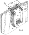
- a plasma chamber 1 shows a section of a plasma chamber 1, which is surrounded by a housing 2.
- a substrate 3 In the lower area of the housing 2 there is a substrate 3 on a turntable 4.
- a magnetron cathode 5 Above the substrate 3, which is to be etched or coated, a magnetron cathode 5 is provided, which in turn has three permanent magnets 6, 7, 8, a yoke 9 and a cathode tub 10 has.
- the cathode tub 10 rests on insulators 11, 12 which are provided with seals 13, 14. These insulators 11, 12 are embedded in the top of the housing 2.
- the negative pole of a direct current supply 15, the positive pole of which is connected to the housing mass of the recipient 2 lies on the electrode trough 10.
- a high-frequency supply 16 can also be provided.
- Beneath the cathode trough 10 there is a target 17 through which the magnetic field lines 18, 19 of the permanent magnets 6 to 8 pass.
- An L-shaped shield 20, 21
- the coil 24 is a coil for generating an additional magnetic field in the plasma space. It is preferably operated with direct current.
- An insulator 26, 27 is provided in front of the vertical part 22, 23 and has grooves in which there is a further coil 28 which is connected to a high-frequency source 29.
- the insulator 26, 27 is closed on its underside by a horizontal part 30, 31 behind the shield 20, 21.
- This part of the shield 20, 21 is electrically insulated and can either be grounded or connected to any electrical potential. It represents the effective anode of the device and can also be used as a distribution screen.
- a cover plate 32, 33 made of an insulating material, for.
- the high-frequency source 29 uses the antenna coil 28 to generate electromagnetic waves in the plasma space, which become Whistler waves can train. The interaction of the electromagnetic waves of the coil 28 with the field of the coil 24 leads to the excitation of helicon modes in the plasma.
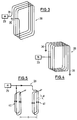
- Fig. 2 shows the magnetron cathode 5 with the shield 20, 21 and the two coils 24 and 28. It can be seen clearly that the coils 24, 28 are embedded in the shield 20, 21 or wrap them around such that the Magnetic fields arising when current flows through are perpendicular to the target 17.
- the substrate 3 and the turntable 4 are omitted in FIG. 2.
- the supply sources 25 and 29 are shown inside the housing 2, although they are actually outside this housing 2, as shown in FIG. 1.
- FIG. 3 to 5 show a more detailed illustration of the high-frequency coil 28.
- the coil 28 is wound clockwise and has one end connected to ground or earth, while its other end 36 is connected to the high-frequency source 29.
- both ends 35, 36 of the coil 28 are connected to earth or ground, while the high-frequency source 29 is connected to the center of the coil 28.
- the coil 28 is divided into two halves 40, 41, the winding direction of these two halves 40, 41 being opposite. Both halves are embedded in the grooves of an insulator at a certain distance from one another. One of these halves 40 is embedded in the insulator part 26, while the other half 41 lies in the grooves of the insulator part 27.
- the winding direction of the coil halves 40, 41 is such that their magnetic fields run parallel to the surface of the target 17.
- D is the slot width, while a is the distance between the coil sections 40, 41.
Landscapes
- Physics & Mathematics (AREA)
- Engineering & Computer Science (AREA)
- Plasma & Fusion (AREA)
- Chemical & Material Sciences (AREA)
- Analytical Chemistry (AREA)
- Physical Vapour Deposition (AREA)
- Electrodes Of Semiconductors (AREA)
- Physical Deposition Of Substances That Are Components Of Semiconductor Devices (AREA)
- Plasma Technology (AREA)
Applications Claiming Priority (2)
| Application Number | Priority Date | Filing Date | Title |
|---|---|---|---|
| DE4235064 | 1992-10-17 | ||
| DE4235064A DE4235064A1 (de) | 1992-10-17 | 1992-10-17 | Vorrichtung zum Erzeugen eines Plasmas mittels Kathodenzerstäubung |
Publications (2)
| Publication Number | Publication Date |
|---|---|
| EP0593924A1 true EP0593924A1 (fr) | 1994-04-27 |
| EP0593924B1 EP0593924B1 (fr) | 1996-02-28 |
Family
ID=6470713
Family Applications (1)
| Application Number | Title | Priority Date | Filing Date |
|---|---|---|---|
| EP93115314A Expired - Lifetime EP0593924B1 (fr) | 1992-10-17 | 1993-09-23 | Dispositif pour la production d'un plasma au moyen d'une pulvérisation cathodique |
Country Status (5)
| Country | Link |
|---|---|
| US (1) | US5417834A (fr) |
| EP (1) | EP0593924B1 (fr) |
| JP (1) | JP3516054B2 (fr) |
| KR (1) | KR100228534B1 (fr) |
| DE (2) | DE4235064A1 (fr) |
Cited By (21)
| Publication number | Priority date | Publication date | Assignee | Title |
|---|---|---|---|---|
| EP0648069A1 (fr) * | 1993-07-30 | 1995-04-12 | Texas Instruments Incorporated | Source de plasma à induction RF pour traitements au plasma |
| WO1996018208A1 (fr) * | 1994-12-06 | 1996-06-13 | Lam Research Corporation | Processeur au plasma pour pieces de grandes dimensions |
| EP0727923A1 (fr) * | 1995-02-15 | 1996-08-21 | Applied Materials, Inc. | Modifications dans, ou qui se rapportent à, des réacteurs à plasma et procédés de fonctionnement correspondants |
| DE19518374A1 (de) * | 1995-05-23 | 1996-11-28 | Forschungszentrum Juelich Gmbh | Verfahren zur hochfrequenzbetriebenen Magnetron-Glimmentladungsionisation, sowie Ionenquelle |
| WO1997042648A1 (fr) * | 1996-05-09 | 1997-11-13 | Applied Materials, Inc. | Bobinage a evidement servant a generer un plasma |
| EP0837490A3 (fr) * | 1996-10-17 | 1998-09-16 | Applied Materials, Inc. | Méthode pour éviter la pulvérisation de l'enroulement dans une source de plasma à couplage inductif (ICP) |
| EP0836219A3 (fr) * | 1996-10-08 | 1998-09-16 | Applied Materials, Inc. | Ecran actif de génération d'un plasma pour la pulvérisation |
| EP0836218A3 (fr) * | 1996-10-08 | 1998-09-16 | Applied Materials, Inc. | Ecran actif de génération d'un plasma pour la pulvérisation |
| WO1998048444A1 (fr) * | 1997-04-21 | 1998-10-29 | Tokyo Electron Arizona, Inc. | Procede et dispositif de pulverisation par bombardement ionique sur un materiau |
| US5948215A (en) * | 1997-04-21 | 1999-09-07 | Tokyo Electron Limited | Method and apparatus for ionized sputtering |
| EP0841683A3 (fr) * | 1996-10-08 | 1999-12-01 | Applied Materials, Inc. | Ecran actif de génération d'un plasma pour la pulvérisation |
| US6080287A (en) * | 1998-05-06 | 2000-06-27 | Tokyo Electron Limited | Method and apparatus for ionized physical vapor deposition |
| US6190513B1 (en) | 1997-05-14 | 2001-02-20 | Applied Materials, Inc. | Darkspace shield for improved RF transmission in inductively coupled plasma sources for sputter deposition |
| US6197165B1 (en) | 1998-05-06 | 2001-03-06 | Tokyo Electron Limited | Method and apparatus for ionized physical vapor deposition |
| US6237526B1 (en) | 1999-03-26 | 2001-05-29 | Tokyo Electron Limited | Process apparatus and method for improving plasma distribution and performance in an inductively coupled plasma |
| US6254746B1 (en) | 1996-05-09 | 2001-07-03 | Applied Materials, Inc. | Recessed coil for generating a plasma |
| US6264812B1 (en) | 1995-11-15 | 2001-07-24 | Applied Materials, Inc. | Method and apparatus for generating a plasma |
| US6287435B1 (en) | 1998-05-06 | 2001-09-11 | Tokyo Electron Limited | Method and apparatus for ionized physical vapor deposition |
| US6474258B2 (en) | 1999-03-26 | 2002-11-05 | Tokyo Electron Limited | Apparatus and method for improving plasma distribution and performance in an inductively coupled plasma |
| US6494998B1 (en) | 2000-08-30 | 2002-12-17 | Tokyo Electron Limited | Process apparatus and method for improving plasma distribution and performance in an inductively coupled plasma using an internal inductive element |
| CN111096082A (zh) * | 2017-10-23 | 2020-05-01 | 株式会社国际电气 | 基板处理装置、半导体装置的制造方法和记录介质 |
Families Citing this family (33)
| Publication number | Priority date | Publication date | Assignee | Title |
|---|---|---|---|---|
| JP3146112B2 (ja) * | 1993-12-24 | 2001-03-12 | シャープ株式会社 | プラズマcvd装置 |
| JP3419899B2 (ja) * | 1994-07-26 | 2003-06-23 | 東京エレクトロン株式会社 | スパッタリング方法及びスパッタリング装置 |
| DE19510736A1 (de) * | 1995-03-24 | 1996-09-26 | Leybold Ag | Vorrichtung zum Verhindern von Überschlägen in Hochfrequenz-Sputteranlagen |
| DE19606375A1 (de) * | 1996-02-21 | 1997-08-28 | Balzers Prozes Systeme Gmbh | Plasmaquelle mit eingekoppelten Whistler- oder Helikonwellen |
| US5716505A (en) * | 1996-02-23 | 1998-02-10 | Balzers Prozess-Systems Gmbh | Apparatus for coating substrates by cathode sputtering with a hollow target |
| US5917286A (en) | 1996-05-08 | 1999-06-29 | Advanced Energy Industries, Inc. | Pulsed direct current power supply configurations for generating plasmas |
| KR100489918B1 (ko) * | 1996-05-09 | 2005-08-04 | 어플라이드 머티어리얼스, 인코포레이티드 | 플라즈마발생및스퍼터링용코일 |
| US6368469B1 (en) * | 1996-05-09 | 2002-04-09 | Applied Materials, Inc. | Coils for generating a plasma and for sputtering |
| US6254747B1 (en) * | 1996-12-25 | 2001-07-03 | Nihon Shinku Gijutsu Kabushiki Kaisha | Magnetron sputtering source enclosed by a mirror-finished metallic cover |
| US6103070A (en) * | 1997-05-14 | 2000-08-15 | Applied Materials, Inc. | Powered shield source for high density plasma |
| US6361661B2 (en) * | 1997-05-16 | 2002-03-26 | Applies Materials, Inc. | Hybrid coil design for ionized deposition |
| US5897753A (en) * | 1997-05-28 | 1999-04-27 | Advanced Energy Industries, Inc. | Continuous deposition of insulating material using multiple anodes alternated between positive and negative voltages |
| US6565717B1 (en) | 1997-09-15 | 2003-05-20 | Applied Materials, Inc. | Apparatus for sputtering ionized material in a medium to high density plasma |
| JPH11135438A (ja) * | 1997-10-28 | 1999-05-21 | Nippon Asm Kk | 半導体プラズマ処理装置 |
| US6132566A (en) * | 1998-07-30 | 2000-10-17 | Applied Materials, Inc. | Apparatus and method for sputtering ionized material in a plasma |
| US6231725B1 (en) * | 1998-08-04 | 2001-05-15 | Applied Materials, Inc. | Apparatus for sputtering material onto a workpiece with the aid of a plasma |
| US6238528B1 (en) | 1998-10-13 | 2001-05-29 | Applied Materials, Inc. | Plasma density modulator for improved plasma density uniformity and thickness uniformity in an ionized metal plasma source |
| US6409890B1 (en) | 1999-07-27 | 2002-06-25 | Applied Materials, Inc. | Method and apparatus for forming a uniform layer on a workpiece during sputtering |
| US6818103B1 (en) | 1999-10-15 | 2004-11-16 | Advanced Energy Industries, Inc. | Method and apparatus for substrate biasing in multiple electrode sputtering systems |
| TW503442B (en) * | 2000-02-29 | 2002-09-21 | Applied Materials Inc | Coil and coil support for generating a plasma |
| GB2377228C (en) * | 2000-07-27 | 2010-01-08 | Trikon Holdings Ltd | Magnetron sputtering |
| JP4871442B2 (ja) * | 2000-09-12 | 2012-02-08 | 株式会社アルバック | 緻密な硬質薄膜の形成装置及び硬質薄膜の形成方法 |
| US6846396B2 (en) * | 2002-08-08 | 2005-01-25 | Applied Materials, Inc. | Active magnetic shielding |
| DE102008022181B4 (de) | 2008-05-05 | 2019-05-02 | Arianegroup Gmbh | Ionentriebwerk |
| DE102008023027B4 (de) * | 2008-05-09 | 2012-06-28 | Von Ardenne Anlagentechnik Gmbh | Elektrodenanordnung für magnetfeldgeführte plasmagestützte Prozesse im Vakuum |
| JP5702143B2 (ja) * | 2008-08-28 | 2015-04-15 | 株式会社イー・エム・ディー | スパッタリング薄膜形成装置 |
| JP5344609B2 (ja) * | 2009-09-04 | 2013-11-20 | サンユー電子株式会社 | イオン化スパッタ真空ポンプ |
| JP5475506B2 (ja) * | 2010-02-26 | 2014-04-16 | 株式会社イー・エム・ディー | スパッタリング薄膜形成装置 |
| KR101151223B1 (ko) * | 2010-06-25 | 2012-06-14 | 한국과학기술원 | 헬리콘 플라즈마 장치 |
| CN103764868B (zh) * | 2011-08-30 | 2017-10-24 | 株式会社Emd | 溅射薄膜形成装置 |
| TWI553138B (zh) * | 2011-08-30 | 2016-10-11 | Emd Corp | Sputtering film forming device |
| DE102015121518A1 (de) * | 2015-12-10 | 2017-06-14 | Technische Universität Clausthal | Verfahren und Anlage zur Herstellung von Beschichtungen auf Substraten sowie ein beschichtetes drahtförmiges Substrat |
| US10867776B2 (en) * | 2018-05-09 | 2020-12-15 | Applied Materials, Inc. | Physical vapor deposition in-chamber electro-magnet |
Citations (5)
| Publication number | Priority date | Publication date | Assignee | Title |
|---|---|---|---|---|
| WO1986006923A1 (fr) * | 1985-05-03 | 1986-11-20 | The Australian National University | Procede et appareil de production de plasmas magnetiques de grand volume |
| EP0271341A2 (fr) * | 1986-12-11 | 1988-06-15 | Dobson, Christopher David | Procédé et dispositif d'attaque par ions |
| EP0403418A2 (fr) * | 1989-06-13 | 1990-12-19 | PLASMA & MATERIALS TECHNOLOGIES, INC. | Dispositif de déposition et gravure à plasma à haute densité |
| WO1992007969A1 (fr) * | 1990-10-31 | 1992-05-14 | International Business Machines Corporation | Appareil servant a deposer un materiau dans des trous dont le rapport d'elancement est eleve |
| DE4042289A1 (de) * | 1990-12-31 | 1992-07-02 | Leybold Ag | Verfahren und vorrichtung zum reaktiven beschichten eines substrats |
Family Cites Families (4)
| Publication number | Priority date | Publication date | Assignee | Title |
|---|---|---|---|---|
| DE3624480A1 (de) * | 1986-07-19 | 1988-01-28 | Leybold Heraeus Gmbh & Co Kg | Zerstaeubungskatode fuer vakuum-beschichtungsanlagen |
| DE4042298A1 (de) * | 1990-12-31 | 1992-07-02 | Schreiber Hans | Verfahren und vorrichtung zum mischen niedrig- bis hochviskoser medien |
| DE4123274C2 (de) * | 1991-07-13 | 1996-12-19 | Leybold Ag | Vorrichtung zum Beschichten von Bauteilen bzw. Formteilen durch Kathodenzerstäubung |
| US5279669A (en) * | 1991-12-13 | 1994-01-18 | International Business Machines Corporation | Plasma reactor for processing substrates comprising means for inducing electron cyclotron resonance (ECR) and ion cyclotron resonance (ICR) conditions |
-
1992
- 1992-10-17 DE DE4235064A patent/DE4235064A1/de not_active Withdrawn
-
1993
- 1993-09-23 DE DE59301719T patent/DE59301719D1/de not_active Expired - Lifetime
- 1993-09-23 EP EP93115314A patent/EP0593924B1/fr not_active Expired - Lifetime
- 1993-09-24 US US08/126,972 patent/US5417834A/en not_active Expired - Lifetime
- 1993-10-14 KR KR1019930021324A patent/KR100228534B1/ko not_active Expired - Fee Related
- 1993-10-18 JP JP26019793A patent/JP3516054B2/ja not_active Expired - Fee Related
Patent Citations (5)
| Publication number | Priority date | Publication date | Assignee | Title |
|---|---|---|---|---|
| WO1986006923A1 (fr) * | 1985-05-03 | 1986-11-20 | The Australian National University | Procede et appareil de production de plasmas magnetiques de grand volume |
| EP0271341A2 (fr) * | 1986-12-11 | 1988-06-15 | Dobson, Christopher David | Procédé et dispositif d'attaque par ions |
| EP0403418A2 (fr) * | 1989-06-13 | 1990-12-19 | PLASMA & MATERIALS TECHNOLOGIES, INC. | Dispositif de déposition et gravure à plasma à haute densité |
| WO1992007969A1 (fr) * | 1990-10-31 | 1992-05-14 | International Business Machines Corporation | Appareil servant a deposer un materiau dans des trous dont le rapport d'elancement est eleve |
| DE4042289A1 (de) * | 1990-12-31 | 1992-07-02 | Leybold Ag | Verfahren und vorrichtung zum reaktiven beschichten eines substrats |
Cited By (30)
| Publication number | Priority date | Publication date | Assignee | Title |
|---|---|---|---|---|
| EP0648069A1 (fr) * | 1993-07-30 | 1995-04-12 | Texas Instruments Incorporated | Source de plasma à induction RF pour traitements au plasma |
| US5430355A (en) * | 1993-07-30 | 1995-07-04 | Texas Instruments Incorporated | RF induction plasma source for plasma processing |
| WO1996018208A1 (fr) * | 1994-12-06 | 1996-06-13 | Lam Research Corporation | Processeur au plasma pour pieces de grandes dimensions |
| US5589737A (en) * | 1994-12-06 | 1996-12-31 | Lam Research Corporation | Plasma processor for large workpieces |
| EP0929093A3 (fr) * | 1994-12-06 | 2003-05-14 | Lam Research Corporation | Processeur au plasma pour pièces de grandes dimensions |
| EP0727923A1 (fr) * | 1995-02-15 | 1996-08-21 | Applied Materials, Inc. | Modifications dans, ou qui se rapportent à, des réacteurs à plasma et procédés de fonctionnement correspondants |
| US5688357A (en) * | 1995-02-15 | 1997-11-18 | Applied Materials, Inc. | Automatic frequency tuning of an RF power source of an inductively coupled plasma reactor |
| DE19518374A1 (de) * | 1995-05-23 | 1996-11-28 | Forschungszentrum Juelich Gmbh | Verfahren zur hochfrequenzbetriebenen Magnetron-Glimmentladungsionisation, sowie Ionenquelle |
| US6264812B1 (en) | 1995-11-15 | 2001-07-24 | Applied Materials, Inc. | Method and apparatus for generating a plasma |
| US6297595B1 (en) | 1995-11-15 | 2001-10-02 | Applied Materials, Inc. | Method and apparatus for generating a plasma |
| WO1997042648A1 (fr) * | 1996-05-09 | 1997-11-13 | Applied Materials, Inc. | Bobinage a evidement servant a generer un plasma |
| US6254746B1 (en) | 1996-05-09 | 2001-07-03 | Applied Materials, Inc. | Recessed coil for generating a plasma |
| EP0836218A3 (fr) * | 1996-10-08 | 1998-09-16 | Applied Materials, Inc. | Ecran actif de génération d'un plasma pour la pulvérisation |
| EP0841683A3 (fr) * | 1996-10-08 | 1999-12-01 | Applied Materials, Inc. | Ecran actif de génération d'un plasma pour la pulvérisation |
| EP0836219A3 (fr) * | 1996-10-08 | 1998-09-16 | Applied Materials, Inc. | Ecran actif de génération d'un plasma pour la pulvérisation |
| US6254737B1 (en) | 1996-10-08 | 2001-07-03 | Applied Materials, Inc. | Active shield for generating a plasma for sputtering |
| US6514390B1 (en) | 1996-10-17 | 2003-02-04 | Applied Materials, Inc. | Method to eliminate coil sputtering in an ICP source |
| EP0837490A3 (fr) * | 1996-10-17 | 1998-09-16 | Applied Materials, Inc. | Méthode pour éviter la pulvérisation de l'enroulement dans une source de plasma à couplage inductif (ICP) |
| US5948215A (en) * | 1997-04-21 | 1999-09-07 | Tokyo Electron Limited | Method and apparatus for ionized sputtering |
| WO1998048444A1 (fr) * | 1997-04-21 | 1998-10-29 | Tokyo Electron Arizona, Inc. | Procede et dispositif de pulverisation par bombardement ionique sur un materiau |
| US6190513B1 (en) | 1997-05-14 | 2001-02-20 | Applied Materials, Inc. | Darkspace shield for improved RF transmission in inductively coupled plasma sources for sputter deposition |
| US6080287A (en) * | 1998-05-06 | 2000-06-27 | Tokyo Electron Limited | Method and apparatus for ionized physical vapor deposition |
| US6287435B1 (en) | 1998-05-06 | 2001-09-11 | Tokyo Electron Limited | Method and apparatus for ionized physical vapor deposition |
| US6197165B1 (en) | 1998-05-06 | 2001-03-06 | Tokyo Electron Limited | Method and apparatus for ionized physical vapor deposition |
| US6474258B2 (en) | 1999-03-26 | 2002-11-05 | Tokyo Electron Limited | Apparatus and method for improving plasma distribution and performance in an inductively coupled plasma |
| US6237526B1 (en) | 1999-03-26 | 2001-05-29 | Tokyo Electron Limited | Process apparatus and method for improving plasma distribution and performance in an inductively coupled plasma |
| US6719886B2 (en) | 1999-11-18 | 2004-04-13 | Tokyo Electron Limited | Method and apparatus for ionized physical vapor deposition |
| US6494998B1 (en) | 2000-08-30 | 2002-12-17 | Tokyo Electron Limited | Process apparatus and method for improving plasma distribution and performance in an inductively coupled plasma using an internal inductive element |
| CN111096082A (zh) * | 2017-10-23 | 2020-05-01 | 株式会社国际电气 | 基板处理装置、半导体装置的制造方法和记录介质 |
| CN111096082B (zh) * | 2017-10-23 | 2022-11-18 | 株式会社国际电气 | 基板处理装置、半导体装置的制造方法和记录介质 |
Also Published As
| Publication number | Publication date |
|---|---|
| EP0593924B1 (fr) | 1996-02-28 |
| JP3516054B2 (ja) | 2004-04-05 |
| KR940010868A (ko) | 1994-05-26 |
| KR100228534B1 (ko) | 1999-11-01 |
| JPH06240452A (ja) | 1994-08-30 |
| DE4235064A1 (de) | 1994-04-21 |
| US5417834A (en) | 1995-05-23 |
| DE59301719D1 (de) | 1996-04-04 |
Similar Documents
| Publication | Publication Date | Title |
|---|---|---|
| EP0593924B1 (fr) | Dispositif pour la production d'un plasma au moyen d'une pulvérisation cathodique | |
| DE2556607C2 (de) | Verfahren und Vorrichtung zur Kathodenzerstäubung | |
| DE69504254T2 (de) | Vorrichtung und Verfahren zur Halbleitersbearbeitung | |
| DE69128195T2 (de) | Ionenplattierung mittels magnetronsputtern | |
| DE69019741T2 (de) | Ionenstrahlkanone. | |
| DE69421033T2 (de) | RF induktive Plasmaquelle zur Plasmabehandlung | |
| DE69320151T2 (de) | Flachen magnetronzerstäubungsanlage | |
| EP2050120B1 (fr) | Source de plasma ecr | |
| DE69732364T2 (de) | Ionenquelle | |
| DE69207212T2 (de) | Hochfrequenz-ionenquelle | |
| DE69123528T2 (de) | Gerät und Verfahren unter Verwendung eines durch Mikrowellen erzeugten Plasmas | |
| DE4102102A1 (de) | Magnetanordnung mit dauermagneten | |
| DE112009001457T5 (de) | Sputter-Vorrichtung | |
| EP0772223B1 (fr) | Dispositif pour revêtir un substrat à partir de cibles conductrices d'électricité | |
| EP1290926B1 (fr) | Source de plasma haute frequence | |
| DE4230291C2 (de) | Mikrowellenunterstützte Zerstäubungsanordnung | |
| DE19939040A1 (de) | Magnetronsputtergerät | |
| DE2837594A1 (de) | Vorrichtung zur mikro-bearbeitung mittels ionenerosion | |
| DE4230290A1 (de) | Vorrichtung zum Erzeugen eines Plasmas mittels Kathodenzerstäubung und Mikrowelleneinstrahlung | |
| DE60021167T2 (de) | Vorrichtung zur Erzeugung von Plasma mit hoher Dichte | |
| DE68909262T2 (de) | Vorrichtung für RF-Plasma-Verarbeitung. | |
| DE10358505B4 (de) | Plasmaquelle zur Erzeugung eines induktiv gekoppelten Plasmas | |
| EP0563609B1 (fr) | Dispositif pour la production d'un plasma au moyen d'une pulvérisation cathodique et d'un rayonnement microondes | |
| DE3837487A1 (de) | Verfahren und vorrichtung zum aetzen von substraten mit einer magnetfeldunterstuetzten niederdruck-entladung | |
| DE3411536A1 (de) | Magnetronkatode fuer katodenzerstaeubungsanlagen |
Legal Events
| Date | Code | Title | Description |
|---|---|---|---|
| PUAI | Public reference made under article 153(3) epc to a published international application that has entered the european phase |
Free format text: ORIGINAL CODE: 0009012 |
|
| AK | Designated contracting states |
Kind code of ref document: A1 Designated state(s): CH DE FR GB LI NL |
|
| 17P | Request for examination filed |
Effective date: 19941012 |
|
| 17Q | First examination report despatched |
Effective date: 19950724 |
|
| GRAA | (expected) grant |
Free format text: ORIGINAL CODE: 0009210 |
|
| AK | Designated contracting states |
Kind code of ref document: B1 Designated state(s): CH DE FR GB LI NL |
|
| REG | Reference to a national code |
Ref country code: CH Ref legal event code: NV Representative=s name: PATENTANWALTSBUERO FELDMANN AG |
|
| REF | Corresponds to: |
Ref document number: 59301719 Country of ref document: DE Date of ref document: 19960404 |
|
| ET | Fr: translation filed | ||
| GBT | Gb: translation of ep patent filed (gb section 77(6)(a)/1977) |
Effective date: 19960325 |
|
| RAP2 | Party data changed (patent owner data changed or rights of a patent transferred) |
Owner name: BALZERS UND LEYBOLD DEUTSCHLAND HOLDING AKTIENGESE |
|
| NLT2 | Nl: modifications (of names), taken from the european patent patent bulletin |
Owner name: BALZERS UND LEYBOLD DEUTSCHLAND HOLDING AKTIENGESE |
|
| PLBE | No opposition filed within time limit |
Free format text: ORIGINAL CODE: 0009261 |
|
| 26N | No opposition filed | ||
| REG | Reference to a national code |
Ref country code: GB Ref legal event code: IF02 |
|
| REG | Reference to a national code |
Ref country code: CH Ref legal event code: PFA Owner name: LEYBOLD AKTIENGESELLSCHAFT Free format text: LEYBOLD AKTIENGESELLSCHAFT#WILHELM-ROHN-STRASSE 25, POSTFACH 1555#D-63450 HANAU (DE) -TRANSFER TO- LEYBOLD AKTIENGESELLSCHAFT#WILHELM-ROHN-STRASSE 25, POSTFACH 1555#D-63450 HANAU (DE) |
|
| PGFP | Annual fee paid to national office [announced via postgrant information from national office to epo] |
Ref country code: CH Payment date: 20100923 Year of fee payment: 18 |
|
| PGFP | Annual fee paid to national office [announced via postgrant information from national office to epo] |
Ref country code: FR Payment date: 20101005 Year of fee payment: 18 |
|
| PGFP | Annual fee paid to national office [announced via postgrant information from national office to epo] |
Ref country code: GB Payment date: 20100921 Year of fee payment: 18 |
|
| PGFP | Annual fee paid to national office [announced via postgrant information from national office to epo] |
Ref country code: NL Payment date: 20100916 Year of fee payment: 18 |
|
| PGFP | Annual fee paid to national office [announced via postgrant information from national office to epo] |
Ref country code: DE Payment date: 20100922 Year of fee payment: 18 |
|
| REG | Reference to a national code |
Ref country code: NL Ref legal event code: V1 Effective date: 20120401 |
|
| REG | Reference to a national code |
Ref country code: CH Ref legal event code: PL |
|
| GBPC | Gb: european patent ceased through non-payment of renewal fee |
Effective date: 20110923 |
|
| REG | Reference to a national code |
Ref country code: FR Ref legal event code: ST Effective date: 20120531 |
|
| REG | Reference to a national code |
Ref country code: DE Ref legal event code: R119 Ref document number: 59301719 Country of ref document: DE Effective date: 20120403 |
|
| PG25 | Lapsed in a contracting state [announced via postgrant information from national office to epo] |
Ref country code: CH Free format text: LAPSE BECAUSE OF NON-PAYMENT OF DUE FEES Effective date: 20110930 Ref country code: NL Free format text: LAPSE BECAUSE OF NON-PAYMENT OF DUE FEES Effective date: 20120401 Ref country code: LI Free format text: LAPSE BECAUSE OF NON-PAYMENT OF DUE FEES Effective date: 20110930 Ref country code: DE Free format text: LAPSE BECAUSE OF NON-PAYMENT OF DUE FEES Effective date: 20120403 |
|
| PG25 | Lapsed in a contracting state [announced via postgrant information from national office to epo] |
Ref country code: FR Free format text: LAPSE BECAUSE OF NON-PAYMENT OF DUE FEES Effective date: 20110930 Ref country code: GB Free format text: LAPSE BECAUSE OF NON-PAYMENT OF DUE FEES Effective date: 20110923 |