EP0594345A2 - Lese/Schreibe-Speicher - Google Patents
Lese/Schreibe-Speicher Download PDFInfo
- Publication number
- EP0594345A2 EP0594345A2 EP93308140A EP93308140A EP0594345A2 EP 0594345 A2 EP0594345 A2 EP 0594345A2 EP 93308140 A EP93308140 A EP 93308140A EP 93308140 A EP93308140 A EP 93308140A EP 0594345 A2 EP0594345 A2 EP 0594345A2
- Authority
- EP
- European Patent Office
- Prior art keywords
- memory
- value
- memory cell
- read
- bit
- Prior art date
- Legal status (The legal status is an assumption and is not a legal conclusion. Google has not performed a legal analysis and makes no representation as to the accuracy of the status listed.)
- Withdrawn
Links
Images

Classifications
-
- G—PHYSICS
- G11—INFORMATION STORAGE
- G11C—STATIC STORES
- G11C7/00—Arrangements for writing information into, or reading information out from, a digital store
- G11C7/10—Input/output [I/O] data interface arrangements, e.g. I/O data control circuits, I/O data buffers
- G11C7/1078—Data input circuits, e.g. write amplifiers, data input buffers, data input registers, data input level conversion circuits
-
- G—PHYSICS
- G11—INFORMATION STORAGE
- G11C—STATIC STORES
- G11C11/00—Digital stores characterised by the use of particular electric or magnetic storage elements; Storage elements therefor
- G11C11/21—Digital stores characterised by the use of particular electric or magnetic storage elements; Storage elements therefor using electric elements
- G11C11/34—Digital stores characterised by the use of particular electric or magnetic storage elements; Storage elements therefor using electric elements using semiconductor devices
- G11C11/40—Digital stores characterised by the use of particular electric or magnetic storage elements; Storage elements therefor using electric elements using semiconductor devices using transistors
- G11C11/41—Digital stores characterised by the use of particular electric or magnetic storage elements; Storage elements therefor using electric elements using semiconductor devices using transistors forming static cells with positive feedback, i.e. cells not needing refreshing or charge regeneration, e.g. bistable multivibrator or Schmitt trigger
- G11C11/413—Auxiliary circuits, e.g. for addressing, decoding, driving, writing, sensing, timing or power reduction
- G11C11/417—Auxiliary circuits, e.g. for addressing, decoding, driving, writing, sensing, timing or power reduction for memory cells of the field-effect type
- G11C11/419—Read-write [R-W] circuits
-
- G—PHYSICS
- G11—INFORMATION STORAGE
- G11C—STATIC STORES
- G11C7/00—Arrangements for writing information into, or reading information out from, a digital store
- G11C7/10—Input/output [I/O] data interface arrangements, e.g. I/O data control circuits, I/O data buffers
- G11C7/1051—Data output circuits, e.g. read-out amplifiers, data output buffers, data output registers, data output level conversion circuits
Definitions
- This invention relates to memory circuits and, more particularly, to static random access memory circuits.
- new data to be written to the cells of a memory array are available before existing data is read from those cells. For example, when buffering packets of data during asynchronous transfer mode (ATM) switching, new data packets are presented to memory at the same time as existing packets can be read from memory. In such applications, it would be desirable to read the existing data and write the new data to the memory cells within a single memory cycle, so as to achieve maximum performance for a selected clock speed. It also would be desirable to minimize power consumption during memory operations.
- ATM asynchronous transfer mode
- a static random access memory sometimes referred to herein as a "read/write" memory, by performing both read and write operations within a single memory cycle.
- incoming data are stored immediately in those cells.
- Reduced power consumption is achieved in such memories by preventing the occurrance of a write operation if the value of a bit to be written to a memory cell is the same as the value of the bit currently stared in that memory cell. More particularly, the result of a read operation on a particular memory cell is compared with the data value to be written to that cell to determine whether a subsequent write operation is required. If the value in the cell equals the value to be written, the write operation is not performed.
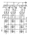
- FIG. 1 shows an array of memory cells arranged in a conventional manner.
- the array of memory cells is arranged in a matrix having n horizontal rows and n vertical columns.
- the memory cells 10 in a given column are coupled by a word select line.
- a single word select line is energized to specify the group of memory cells active during that memory cycle.
- the memory cells within each row are coupled to each other by two bit lines, BIT and BIT.
- Each memory cell 10 has two nodes. One of the two nodes stores an actual data value and is coupled to the bit line "BIT.” The other of the two nodes stores the complement of the data value stored by the first node. This second node is coupled to the bit line "BIT.”
- Each row of memory cells is coupled via its respective bit lines to a control circuit 12.
- Control circuit 12 reads data from and writes data to a selected memory cell, as specified by the word select line (e.g., lines 24 and 26), within the row.
- Control circuit 12 outputs data read from the memory cells to a read bus 14 and receives data to be written to the memory cells from a write bus 16.
- a "select" control line 18 is provided to control circuit 12 to enable read and write operations to be performed on groups or subsets of the memory cells that are coupled to the energized word select line.
- Control circuit 12 Power for control circuit 12 is provided from V dd .
- Control circuit 12 powers the memory cells via the bit lines.
- the memory array operates synchronously, in response to system clock signals input to control circuit 12 via line 22.
- the memory of the invention is utilized within a telecommunications packet switch, such as an ATM switch.
- the memory of the present invention is used to read and write, within a single memory cycle, entire packets of data to selected groups of memory cells.
- the telecommunications switch generates an address that is decoded by a decoder (not shown), using conventional memory addressing techniques, to uniquely identify a group of memory cells 10 that will store a packet of data, with each bit of the data packet being stored in a different one of the memory cells.
- a decoded address typically will correspond to several memory cells that are coupled by a common word select line, such as line 24.
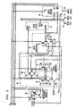
- FIG. 2 shows control circuit 12 in greater detail.
- Control circuit 12 includes a precharge circuit 28, a sense amplifier 30, a latch generator circuit 32, a read latch circuit 34, and a write circuit 36, each of which is described in greater detail below.
- Precharge circuit 28 precharges the bit lines to V dd in the first half of the memory cycle
- sense amplifier 30 detects changes in the voltages on the bit lines, so as to read the data value from the memory cell.
- latch generator circuit 32 When the read is complete, latch generator circuit 32 generates a latch signal and outputs the latch signal simultaneously to read latch circuit 34 to latch the data and to write circuit 36 to initiate a write operation.
- sense amplifier 30 is coupled to the bit lines to detect changes in the voltages on those bit lines. In response to changes in the bit line voltages, sense amplifier 30 determines which of the bit lines is coupled to a logic one and which is coupled to a logic zero. Upon reaching a decision, sense amplifier 30 outputs the data simultaneously to latch generator 32 and read latch 34.
- Latch generator 32 generates a latch signal in response to the output signal from amplifier 30 upon receipt of a system clock signal.
- the latch signal from latch generator 32 is provided simultaneously to read latch 34 and to write circuit 36.
- Read latch 34 latches the signal from sense amplifier 30 upon receiving a latch signal from latch generator 32. Read latch 34 outputs the latched data to read bus 14.
- Write circuit 36 receives incoming data to be written to a memory cell from write bus 16.
- Write circuit 36 initiates the write operation upon receiving the latch signal from latch generator 32 if the write enable line is energized. As will be described below, it is the provision of a common latch signal to read latch 34 and write circuit 36 that enables control circuit 12 to perform both a read and write operation on a memory cell within a single clock cycle.
- Precharge circuit 28 includes enhancement-type P-channel transistors 38, 40, and 42.
- the gate terminal of transistors 38, 40, and 42 are connected to the clock signal.
- the drain of transistors 38 and 42 are connected to V dd .
- the source of transistors 38 and 42 are coupled together through transistor 40.
- the source terminal of transistor 38 is coupled to one bit line (e.g. BIT) and the source terminal of transistor42 is coupled to the other bit line (e.g. BIT).
- precharge circuit 28 could be any circuit which quickly charges the bit lines to V dd upon receipt of a clock signal.
- sense amplifier 30 detects relative changes in the voltages on the bit lines to determine which of the bit lines is connected to a logic one and which is connected to a logic zero, so as to read data from a memory cell 10.
- sense amplifier 30, shown in simplified form in FIG. 3 includes two inverters 45 and 47 that are regeneratively cross-coupled through a balance circuit 52 (shown in greater detail in FIG. 2). As discussed further below, when balance circuit 52 is closed, inverters 45 and 47 remain in an unstable state. Once balance circuit 52 opens, the inverters drive to a stable state in a direction that is determined by the relative voltages on the bit lines. The direction of current flow between the inverters, as determined by the relative voltages on the bit lines, establishes the value of the data to be latched by read latch 34.
- Inverters 45 and 47 are formed by complimentary-symmetry MOS (CMOS) transistors 44 and 46, and transistors 48 and 50, respectively.
- CMOS complimentary-symmetry MOS
- the gates of transistors 44 and 46 are regeneratively coupled to the gates of transistors 48 and 50 through balance circuit 52, comprising transistors 54 and 56.
- the gate terminals of transistors 54 and 56 are controlled by the system clock signal.
- Balance circuit 52 appears to inverters 45 and 47 as a short circuit when the clock signal is low. Conversely, balance circuit 52 appears to inverters 45 and 47 as a open circuit when the clock signal is high.
- Inverters 45 and 47 draw power for circuit operation from the bit lines. This provides an advantage over conventional sense amplifiers, which drew current from supply lines (e.g., V dd ), because the sense amplifierdraws negligible current once it has read the contents of a memory cell.
- supply lines e.g., V dd
- sense amplifier 30 offers several other advantages over conventional sense amplifier designs. For example, sense amplifier 30 discharges the bit lines only slightly during a read operation, leaving the bit lines at a voltage near V dd . This facilitates fast precharging of the bit lines after the sensing operation is completed. Also, sense amplifier 30 is most sensitive around V dd . This simplifies precharging of the bit lines, because V dd is readily available. In contrast, conventional sense amplifier circuits are most sensitive to voltages around V dd /2. Thus, conventional sense amplifiers required additional circuitry, and thus a more complex circuit design, to generate V dd /2. Furthermore, the sense amplifier is comprised of only a single stage, the output of which is a true CMOS voltage. Conventional sense amplifier designs require one or more additional stages, following the sensing stage, to restore output voltages to true CMOS voltages. These additional stages increase manufacturing costs, reduce operating speed, and require additional wafer space.
- Sense amplifier 30 operates as follows. The amplifier is first selected by applying an appropriate voltage to select line 18 to establish a current path between inverters 45 and 47 and V ss through transistor 58. The voltage on the bit linescauses cross-coupled inverters 45 and 47 to remain in an unstable state as long as the cross-connect formed by balance circuit 52 remains in a short circuit state. Upon receipt of a clock signal, balance circuit 52 appears to inverters 45 and 47 as an open circuit, causing the inverters to drive to a stable state in response to the difference in voltage between the bit lines.
- inverters 45 and 47 When the voltage on line BIT is higher than the voltage on line BIT, inverters 45 and 47 will drive the output of inverter 45 high, causing a logic one to be output to the "Data In" terminal of read latch 34. However, when the voltage on BIT is higher than the voltage on BIT, inverters 45 and 47 will drive the output of inverter 45 low, causing a logic zero to be output to the Data In terminal of read latch 34.
- Latch generator circuit 32 causes the control circuit to operate in a synchronous mode by generating a clocked latch signal from the system clock.
- Latch generator circuit 32 includes transistors 60, 62, 64, and 66.
- Latch generator circuit 32 receives the data signals output from sense amplifier 30, together with a system clock signal, and uses these three signals to generate a latch signal.
- the output of sense amplifier 30, comprising the signal read from the memory cell and its inverse, are input to transistors 64 and 66.
- the drain terminals of 64 and 66 are coupled to V dd through the source terminal of transistor 60.
- the source terminals of transistors 64 and 66 are connected to V ss through transistor 62.
- Transistors 60 and 62 are controlled by the clock signal.
- transistors 60 and 62 Upon receipt of a clock signal, transistors 60 and 62 cause current to flow from V dd to V ss when data are presented to latch generator circuit 32, from sense amplifier 30, on transistors 64 and 66. This generates a latch signal at the source terminal of transistor 60. The latch signal is simultaneously provided to read latch 34 and write circuit 36.
- Read latch 34 receives at its Data In terminal the value of the existing contents of the memory cell (i.e., the value on the line BIT). This value is latched upon receipt by the read latch of the latch signal from latch generator circuit 32. Read latch 34 outputs the latched value to read bus 14.
- Read latch 34 can be any suitable circuit, such as a D-type flip-flop.
- Write circuit 36 receives new data to be written to the memory cell via write bus 16. The data on write bus 16 is presented to write circuit 36 prior to the write circuit receiving the latch signal from latch generator 32. Upon receipt of the latch signal, write circuit 36 causes one of the bit lines to be drawn to ground, so as to write the new data to the memory cell. Write circuit 36 operates only when write enable line 20 is energized. It will be apparent to one skilled in the art in view of this disclosure that write circuit 36 can be constructed using any suitable circuitry.
- FIG. 4 shows an exemplary embodiment of a circuit 67 within write circuit 36 for writing to one of the pair of bit lines (i.e., BIT or BIT).
- a corresponding duplicate circuit is provided within write circuit 36 for the other bit line (the signal on the data line is inverted).
- Circuit 67 includes transistors 68, 70, 72, 74, and 76.
- Transistors 68, 70, 72, and 74 provide a current path between V dd and V ss .
- Transistors 68 and 74 are controlled by the latch signal from latch generator 32, while transistors 70 and 72 are controlled by write enable line 20 and data received from write bus 16, respectively.
- Transistor 76 is turned on, driving the bit line to V ss , when the data on write bus 16 is set high and a write is selected simultaneously on write enable line 20. Under these circumstances, the latch signal clocks circuit 67, and a write is performed.
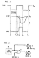
- FIG. 5 illustrates the timing of various signals within the read/write memory.
- the clock signal goes low.
- the low clock signal actuates precharge circuit 28 and closes balance switch 52 by turning on transistors 54 and 56 of sense amplifier 30.
- Precharge circuit 28 charges the bit lines to a voltage of V dd , providing power to sense amplifier circuit 30. (For simplicity, the bit lines are depicted in interval to-t l as already being in their precharged state.)
- the latch signal is low.
- Select line 18 is driven high to select the control circuits 12 required for this memory cycle.
- the clock signal goes high, terminating the precharge of the bit lines.
- a word select line (shown in FIG. 1) is driven high, causing one memory cell from each row of the array to be connected to a different one of control circuits 12 by a respective pair of bit lines. Because the bit lines provide power to sense amplifier 30, the voltage of both bit lines will drop slightly from V dd . However, the memory cell will cause the voltage of one of the bit lines to drop faster than the other. This occurs because one node of the memory cell stores a zero, and thus is connected to ground.
- balance switch 52 is opened, causing inverters 45 and 47 of sense amplifier 30 to drive to a stable state.
- a short delay is provided prior to opening balance switch 52 so as to permit the voltages on the bit lines to sufficiently separate from each other (during interval t l -t 2 ) to facilitate the sensing operation.
- the sensing operation is completed and the latch signal is generated.
- the data value output by sense amplifier 30 is latched in read latch 34 and the write operation is initiated.
- one of the bit lines is pulled to ground, causing a zero to be written to the memory cell node associated with that bit line.
- the other bit line remains charged to a voltage near V dd , causing a one to be written to the memory cell node associated with the second bit line.
- the write operation is complete at t 4 .
- the power consumed by a read/write memory can be greatly reduced by preventing the occurrance of a write operation when the value of a bit to be written to a memory cell is the same as the value of the bit currently stored in that memory cell.
- the content of a selected cell is read immediately prior to writing new data to the cell.
- the result of a read operation on a particular memory cell can be compared with the data to be written to that cell to determine whether a subsequent write operation is required. If the value in the cell equals the value to be written, the write operation is blocked.
- FIG. 6 shows exemplary circuitry for implementing a comparison of the contents of a memory cell following a read operation and data to be written to the cell.
- the circuit includes an exclusive-OR gate 78, one input terminal of which is coupled to the "data" output of sense amplifier 30.
- the other input terminal of exclusive-OR gate 78 is coupled to write bus 16.
- the output terminal of exclusive-OR gate 78 drives write enable 20 of write circuit 36 to enable or disable the write circuit.
- exclusive-OR gate 78 outputs a logic zero to write circuit 36 and thus prevents a write operation.
- exclusive-OR gate 78 outputs a logic one to write circuit 36 and thus enables a write operation.
Landscapes
- Engineering & Computer Science (AREA)
- Microelectronics & Electronic Packaging (AREA)
- Computer Hardware Design (AREA)
- Static Random-Access Memory (AREA)
Applications Claiming Priority (2)
| Application Number | Priority Date | Filing Date | Title |
|---|---|---|---|
| US07/965,138 US5394361A (en) | 1992-10-22 | 1992-10-22 | Read/write memory |
| US965138 | 1992-10-22 |
Publications (2)
| Publication Number | Publication Date |
|---|---|
| EP0594345A2 true EP0594345A2 (de) | 1994-04-27 |
| EP0594345A3 EP0594345A3 (en) | 1994-08-24 |
Family
ID=25509508
Family Applications (1)
| Application Number | Title | Priority Date | Filing Date |
|---|---|---|---|
| EP9393308140A Withdrawn EP0594345A3 (en) | 1992-10-22 | 1993-10-13 | Read/write memory |
Country Status (4)
| Country | Link |
|---|---|
| US (1) | US5394361A (de) |
| EP (1) | EP0594345A3 (de) |
| JP (1) | JPH06203571A (de) |
| KR (1) | KR960004000B1 (de) |
Cited By (1)
| Publication number | Priority date | Publication date | Assignee | Title |
|---|---|---|---|---|
| DE10125393A1 (de) * | 2001-05-23 | 2002-12-12 | Siemens Ag | Verfahren und Anordnung zum energiesparenden Senden von Daten durch einen eine integrierte Schaltung aufnehmenden Baustein über einen daran angeschlossenen Datenbus |
Families Citing this family (13)
| Publication number | Priority date | Publication date | Assignee | Title |
|---|---|---|---|---|
| US5646948A (en) * | 1993-09-03 | 1997-07-08 | Advantest Corporation | Apparatus for concurrently testing a plurality of semiconductor memories in parallel |
| JPH0863975A (ja) * | 1994-08-25 | 1996-03-08 | Fujitsu Ltd | スタティックramおよびこのスタティックramを有する処理装置 |
| US5541918A (en) * | 1995-01-31 | 1996-07-30 | Fore Systems, Inc. | Method and apparatus for manipulating an ATM cell |
| US6262937B1 (en) | 1998-03-13 | 2001-07-17 | Cypress Semiconductor Corp. | Synchronous random access memory having a read/write address bus and process for writing to and reading from the same |
| US6262936B1 (en) | 1998-03-13 | 2001-07-17 | Cypress Semiconductor Corp. | Random access memory having independent read port and write port and process for writing to and reading from the same |
| US6069839A (en) | 1998-03-20 | 2000-05-30 | Cypress Semiconductor Corp. | Circuit and method for implementing single-cycle read/write operation(s), and random access memory including the circuit and/or practicing the method |
| US6087858A (en) * | 1998-06-24 | 2000-07-11 | Cypress Semiconductor Corp. | Self-timed sense amplifier evaluation scheme |
| US5978280A (en) * | 1998-06-25 | 1999-11-02 | Cypress Semiconductor Corp. | Method, architecture and circuit for reducing and/or eliminating small signal voltage swing sensitivity |
| US6122203A (en) * | 1998-06-29 | 2000-09-19 | Cypress Semiconductor Corp. | Method, architecture and circuit for writing to and reading from a memory during a single cycle |
| US5986970A (en) * | 1998-06-29 | 1999-11-16 | Cypress Semiconductor Corp. | Method, architecture and circuit for writing to a memory |
| US5946255A (en) * | 1998-07-31 | 1999-08-31 | Cypress Semiconductor Corp. | Wordline synchronized reference voltage generator |
| US20020174290A1 (en) * | 2001-05-15 | 2002-11-21 | Wu Kun Ho | Memory accelerator, acceleration method and associated interface card and motherboard |
| CN113867287B (zh) * | 2021-09-28 | 2023-12-05 | 浙江华章科技有限公司 | 一种工业数据采集方法及系统 |
Family Cites Families (7)
| Publication number | Priority date | Publication date | Assignee | Title |
|---|---|---|---|---|
| JPS5613573A (en) * | 1979-07-11 | 1981-02-09 | Toshiba Corp | Memory control system |
| US4599708A (en) * | 1983-12-30 | 1986-07-08 | International Business Machines Corporation | Method and structure for machine data storage with simultaneous write and read |
| US4763305A (en) * | 1985-11-27 | 1988-08-09 | Motorola, Inc. | Intelligent write in an EEPROM with data and erase check |
| JPS6379292A (ja) * | 1986-09-24 | 1988-04-09 | Nec Corp | スタテイツク型メモリ |
| US5023838A (en) * | 1988-12-02 | 1991-06-11 | Ncr Corporation | Random access memory device with integral logic capability |
| DE4014151A1 (de) * | 1990-05-02 | 1991-11-07 | Detecon Gmbh | Verfahren zur verlaengerung der benutzungsdauer von informationstraegern mit eeprom |
| US5309395A (en) * | 1992-10-22 | 1994-05-03 | At&T Bell Laboratories | Synchronous static random access memory |
-
1992
- 1992-10-22 US US07/965,138 patent/US5394361A/en not_active Expired - Lifetime
-
1993
- 1993-10-11 KR KR1019930020992A patent/KR960004000B1/ko not_active Expired - Fee Related
- 1993-10-13 EP EP9393308140A patent/EP0594345A3/en not_active Withdrawn
- 1993-10-21 JP JP5285585A patent/JPH06203571A/ja active Pending
Cited By (1)
| Publication number | Priority date | Publication date | Assignee | Title |
|---|---|---|---|---|
| DE10125393A1 (de) * | 2001-05-23 | 2002-12-12 | Siemens Ag | Verfahren und Anordnung zum energiesparenden Senden von Daten durch einen eine integrierte Schaltung aufnehmenden Baustein über einen daran angeschlossenen Datenbus |
Also Published As
| Publication number | Publication date |
|---|---|
| JPH06203571A (ja) | 1994-07-22 |
| KR940010107A (ko) | 1994-05-24 |
| KR960004000B1 (ko) | 1996-03-25 |
| EP0594345A3 (en) | 1994-08-24 |
| US5394361A (en) | 1995-02-28 |
Similar Documents
| Publication | Publication Date | Title |
|---|---|---|
| US5309395A (en) | Synchronous static random access memory | |
| US4417328A (en) | Random access semiconductor memory device using MOS transistors | |
| US4612631A (en) | Static type semiconductor memory circuit | |
| KR100848058B1 (ko) | 셀프 타이밍 회로를 구비하는 정적 기억 장치 | |
| KR100228621B1 (ko) | 기록 주기동안 데이터의 변화에 따라 등화하는 열을 가지는 반도체 메모리 | |
| US7345936B2 (en) | Data storage circuit | |
| US5394361A (en) | Read/write memory | |
| US5850359A (en) | Asynchronous high speed zero DC-current SRAM system | |
| JP2000195271A (ja) | 半導体メモリ装置 | |
| JPS631677B2 (de) | ||
| EP0759621A2 (de) | Leseverstärker für statischen Direktzugriffspeicher | |
| EP0145488A2 (de) | Halbleiterspeicheranordnung | |
| US3938109A (en) | High speed ECL compatible MOS-Ram | |
| US6097618A (en) | Apparatus and method for correcting data in a non-volatile random access memory | |
| EP0547889B1 (de) | Tristate-Treiberschaltung für interne Datenbusleitungen | |
| US6292418B1 (en) | Semiconductor memory device | |
| US5384504A (en) | Sense amplifier powered from bit lines and having regeneratively cross-coupling means | |
| EP0547890A2 (de) | Lese-/Schreibe-Speicher mit verriegelter Schreibsteuerung | |
| US5295104A (en) | Integrated circuit with precharged internal data bus | |
| KR0155986B1 (ko) | 반도체 기억장치 | |
| US5051955A (en) | Semiconductor memory having improved data readout scheme | |
| US5257226A (en) | Integrated circuit with self-biased differential data lines | |
| EP0547892B1 (de) | Integrierte Schaltung mit gegenseitig gesteuerten differenzialen Datenleitungen | |
| EP0199458B1 (de) | Speicherschaltung mit Schreibschema | |
| JP2580086B2 (ja) | スタテイック型半導体記憶装置 |
Legal Events
| Date | Code | Title | Description |
|---|---|---|---|
| PUAI | Public reference made under article 153(3) epc to a published international application that has entered the european phase |
Free format text: ORIGINAL CODE: 0009012 |
|
| AK | Designated contracting states |
Kind code of ref document: A2 Designated state(s): DE FR GB IT |
|
| RAP3 | Party data changed (applicant data changed or rights of an application transferred) |
Owner name: AT&T CORP. |
|
| PUAL | Search report despatched |
Free format text: ORIGINAL CODE: 0009013 |
|
| AK | Designated contracting states |
Kind code of ref document: A3 Designated state(s): DE FR GB IT |
|
| 17P | Request for examination filed |
Effective date: 19950209 |
|
| 17Q | First examination report despatched |
Effective date: 19970403 |
|
| 18W | Application withdrawn |
Withdrawal date: 19970530 |