EP0594852A1 - Circuit a balayage a surete intrinseque et capteur du type a faisceaux a axes optique multiples - Google Patents
Circuit a balayage a surete intrinseque et capteur du type a faisceaux a axes optique multiples Download PDFInfo
- Publication number
- EP0594852A1 EP0594852A1 EP92909797A EP92909797A EP0594852A1 EP 0594852 A1 EP0594852 A1 EP 0594852A1 EP 92909797 A EP92909797 A EP 92909797A EP 92909797 A EP92909797 A EP 92909797A EP 0594852 A1 EP0594852 A1 EP 0594852A1
- Authority
- EP
- European Patent Office
- Prior art keywords
- circuit
- output
- scanning
- fail
- safe
- Prior art date
- Legal status (The legal status is an assumption and is not a legal conclusion. Google has not performed a legal analysis and makes no representation as to the accuracy of the status listed.)
- Granted
Links
Images


Classifications
-
- H—ELECTRICITY
- H03—ELECTRONIC CIRCUITRY
- H03K—PULSE TECHNIQUE
- H03K5/00—Manipulating of pulses not covered by one of the other main groups of this subclass
- H03K5/15—Arrangements in which pulses are delivered at different times at several outputs, i.e. pulse distributors
- H03K5/15013—Arrangements in which pulses are delivered at different times at several outputs, i.e. pulse distributors with more than two outputs
- H03K5/1506—Arrangements in which pulses are delivered at different times at several outputs, i.e. pulse distributors with more than two outputs with parallel driven output stages; with synchronously driven series connected output stages
- H03K5/15066—Arrangements in which pulses are delivered at different times at several outputs, i.e. pulse distributors with more than two outputs with parallel driven output stages; with synchronously driven series connected output stages using bistable devices
-
- H—ELECTRICITY
- H03—ELECTRONIC CIRCUITRY
- H03K—PULSE TECHNIQUE
- H03K17/00—Electronic switching or gating, i.e. not by contact-making and –breaking
- H03K17/94—Electronic switching or gating, i.e. not by contact-making and –breaking characterised by the way in which the control signals are generated
- H03K17/965—Switches controlled by moving an element forming part of the switch
- H03K17/968—Switches controlled by moving an element forming part of the switch using opto-electronic devices
- H03K17/969—Switches controlled by moving an element forming part of the switch using opto-electronic devices having a plurality of control members, e.g. keyboard
-
- H—ELECTRICITY
- H03—ELECTRONIC CIRCUITRY
- H03K—PULSE TECHNIQUE
- H03K2217/00—Indexing scheme related to electronic switching or gating, i.e. not by contact-making or -breaking covered by H03K17/00
- H03K2217/94—Indexing scheme related to electronic switching or gating, i.e. not by contact-making or -breaking covered by H03K17/00 characterised by the way in which the control signal is generated
- H03K2217/941—Indexing scheme related to electronic switching or gating, i.e. not by contact-making or -breaking covered by H03K17/00 characterised by the way in which the control signal is generated using an optical detector
- H03K2217/94114—Optical multi axis
Definitions
- the present invention relates to a fail-safe scanning circuit which can detect an abnormal condition in a drive output for a plurality of driven objects, when the drive output is generated with successive switching to periodically scan drive the driven objects, and also relates to a fail-safe multi-axis light beam-type sensor using in such a fail-safe scanning circuit.
- Multi-axis light beam-type sensors such as disclosed in US Patent No. 4,309,696, have been adopted as a method of ensuring the safety of an operator in situations such as where the operation of a press machine is carried out manually by the operator.
- a multi-axis light beam-type sensor there is a region where it is dangerous for an operator to be present when the press machine is operating, and a security region where it is safe to be present.
- a plurality of light emitting elements and light receiving elements are arranged facing each other so that light beams from the light emitting elements are emitted towards the light receiving elements.
- the spacing of the light emitting elements and the light receiving elements aligned vertically is set narrow (of the order of 2cm), and the light beams from the light emitting elements are spread to a certain degree, they are incident on not only the corresponding light receiving elements but also on other neighboring light receiving elements.
- the frequency of the light beams for each light emitting element is made different, and a filter which extracts only the light beam frequency of the corresponding light emitting elements is provided on the respective light receiving element side.
- a scanning drive system which scan drives the corresponding light emitting elements and light receiving elements with successive switching, so that the respective light emitting elements emit light in continuous succession at different times, with the process being repeated in cycles.
- the scanning circuit for driving a plurality of driven objects with continuous switching, and repeatedly scanning the objects in cycles, comprises; a counting circuit for periodically counting a number of input clock signals equal to the number of driven objects, a scanning output generating circuit for generating a number of scanning output signals equal to the number of driven objects, successively and at different times along a time axis, on the basis of the output signal from the counting circuit, and a fail-safe fault detection circuit for generating, an output of a logic value of "1" corresponding to the high energy condition when the output of the plurality of scanning outputs from the scanning output generating circuit is normal, and outputting a logic value of "0" corresponding to the low energy condition when at least one of abnormal conditions of, the output of the plurality of scanning output signals are overlapped on the time axis, and at least one scanning output signal is not generated in one scanning cycle.
- the fault detection circuit detects this and the output from the fault detection circuit becomes a logic value of "0", indicating the scanning circuit abnormality.
- the scanning output generating circuit may comprise; a first AND gate group made up of a number of AND gates equal to the number of driven objects, for outputting a succession of rectangular wave signals at different times on the time axis, based on the output signals from the counting circuit, a high frequency generating circuit for always outputting a high frequency signal, and a second AND gate group, made up of a number of AND gates equal to the number of driven objects, for taking the output rectangular wave signals from the respective AND gates of the first AND gate group, and the output from the high frequency generating circuit, and outputting high frequency signals from the high frequency generating circuit as scanning output signals, when the rectangular wave signals from the respective AND gates of the first AND gate group have a logic value of "1".
- the fault detection circuit may comprise; a first detection part which detects if the plurality of scanning output signals from the scanning output generating circuit are overlapped on the time axis, and when overlapped, judges the abnormality and gives an output of logic value "0" a second detection part which detects if all of the plurality of scanning output signals from the scanning output generating circuit are generated within one scanning period, and if at least one scanning output signal is not generated, judges the abnormality and gives an output of logic value "0", a logical product operation circuit for carrying out a logical product operation on the output from the first detection part and the second detection part, and an on-delay circuit having a delay period at least greater than the time for one scanning period of the scanning output signal, for generating an output of a logical value of "1" indicating a normal scanning output signal condition, when a logical value of "1" is input from the logical product operation circuit.
- the first detection part comprises; a first adding circuit wherein the respective scanning output signals are voltage doubler rectified and added, and the change and discharge time coefficient for the voltage doubler rectifier is set to correspond to the generating period for one scanning output signal, a first window comparator which generates an output of logic value "1" when the output level of the first adding circuit is approximately equal to the voltage doubler rectified level of one scanning output signal, and a first rectifying circuit for rectifying the output from the first window comparator and outputting to the logical product operation circuit.
- the second detection part comprises; a second adding circuit wherein the respective scanning output signals are voltage doubler rectified and added, and the change and discharge time coefficient for the voltage doubler rectifier is set to correspond to one scanning period of all the scanning output signals, a second window comparator which generates an output of logic value "1" when the output level of the second adding circuit is approximately equal to the added value of all the voltage doubler rectified levels of the scanning output signals, and a second rectifying circuit for rectifying the output from the second window comparator and outputting to the logical product operation circuit.
- the multi-axis light beam-type sensor comprises; first and second fail-safe scanning circuits, driven by mutually common clock signals, each of which consists of the fail-safe scanning circuit as claimed in claim 1, a plurality of light emitting elements for generating light beams, the light emitting elements being scan driven with successive switching by a plurality of high frequency scanning output signals successively output from the first fail-safe scanning circuit, at different timing along a time axis, a plurality of light receiving elements disposed to confront the respective light emitting elements, which generate a light received output of logic value "1" on receipt of a light beam from a respective light emitting element, a plurality of amplifiers which amplify the light received output from the light receiving elements provided to each correspond to a respective light receiving element, and which take as a power source the rectangular wave signal from the second fail-safe scanning circuit, which is generated successively at different times along the time axis and which is synchronized with the scanning output signal from the first fail-safe scanning circuit, a first logical product
- the output of the on-delay circuit becomes a logic value of "0", and remains in that condition. Also, with a fault on the scanning circuit side, the output of the first logical product operation circuit becomes a logic value of "0", and the output from the on-delay circuit is also set to a logic value of "0".
- the frequency of the scanning output signals from the first fail-safe scanning circuit, which are applied to the respective light emitting elements is made so that the frequency for the last scanned light emitting element in the scanning period is different to that for the other light emitting elements, then the synchronizing of the last light emitting element with the last light receiving element can be verified for each scanning cycle.
- a fail-safe circuit can be constructed to incorporate the following; a third logical product operation circuit for carrying out a logical product operation on the output from the failure detection circuit in the first fail-safe scanning circuit, and the last scanning output signal in the scanning period, a fourth logical product operation circuit for carrying out a logical product operation on the logical sum of the amplified received light outputs from the plurality of amplifiers corresponding to the light receiving elements, and the last rectangular wave signal in the scanning period of the second fail safe scanning circuit, a fifth logical product operation circuit for carrying out a logical product operation on the output from the third logical product operation circuit, and the output from the fourth logical product operation circuit, and an off-delay circuit which has a time delay which is at least greater than the time for one period of the scanning output signals, and wherein an output of logic value "1" is stopped when an output of logic value of "1" from the fifth logical product operation circuit is stopped.
- FIG. 1 is a overall block diagram of a first embodiment of a fail-safe scanning circuit, according to the present invention.
- FIG. 2 is a block diagram showing an example of a counting circuit structure for the embodiment of FIG. 1.
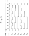
- FIG. 3 is a time chart for the counting circuit output.
- FIG. 4 is a block diagram of a scanning output generating circuit for the embodiment of FIG. 1.
- FIG. 5 is time chart for the rectangular wave signal and scanning output signal from the scanning output generating circuit.
- FIG. 6 is a block diagram of a fault detection circuit of the embodiment of FIG. 1.
- FIG. 7 is a block diagram of a scanning output generating circuit for a first embodiment of a multi-axis light beam-type sensor, according to the present invention.
- FIG. 8 is a block diagram of the sensor circuit of the first embodiment of FIG. 7.
- FIG. 9 is a block diagram of a sensor circuit for a second embodiment of a multi-axis light beam-type sensor.
- FIG. 10 is a schematic diagram showing an example of a structure of an off-delay circuit used in the sensor circuit of the second embodiment of FIG 9.
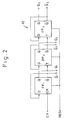
- FIG. 2 shows details of the before-mentioned counting circuit 10.
- the counting circuit 10 of the present embodiment comprises three flip flops FF1, FF2 and FF3 making up a binary counter.
- the counting circuit 10 periodically counts the clock signals CK with eight clock signals CK for one period, and gives a count result expressed in binary numbers of "0","1" as combinations of the outputs from the positive terminals Q1, Q2, Q3 and the inversion terminals Q1, Q2, Q3 of the flip flops FF1, FF2, FF3.
- the timing for operation of the flip flops FF1, FF2, FF3 is shown in FIG. 3.
- FIG. 4 illustrates a construction of the scanning output generating circuit 20.
- a first AND gate group 21 made up of a plurality of 3-input AND gates GA i
- the operation of the scanning output generating circuit 20 is as follows.
- the six outputs from the counting circuit 10 are made into combinations of three outputs to give eight signals, which are input respectively to the AND gates GA i of the first AND gate group 21.
- the initial clock signal CK input to the counting circuit 10 initially gives a high logic level (logical value of "1") output from the AND gate GA1.
- the output from the AND gate GA1 becomes a low logic level (logical value of "0")
- the output from the AND gate GA2 becomes a logical value of "1".
- the operation is executed for each of the clock signal CK inputs, with the outputs of AND gate GA3 through AND gate GA8, changing successively to a logical value of "1", giving an output for the first AND gate group 21 as a series of rectangular wave signals t1 through t8 along the time axis as shown in FIG. 5.
- the ninth clock signal CK then returns the AND gate GA1 to the initial condition, to once more generate an output of logical value of "1". Accordingly, the eight clock signals CK generate a periodic succession of rectangular wave signals t i over one period.
- the respective AND gates GB i of the second AND gate group 23 take the rectangular wave signal t i , and when this has a logical value "1" condition, change it into a high-frequency signal of the frequency f1 output from high-frequency generating circuit 22, and then output this. Accordingly, a succession of high-frequency scanning output signals P i along the time axis as shown in FIG. 5 are generated continuously and repeatedly from the second AND gate group 23.
- FIG. 6 shows the construction of the fault detection circuit 30.
- the fault detection circuit 30 shown in FIG. 6 comprises the following components.
- Fail-safe first and second window comparators WC1, WC2 see for example US Patent No. 4,661,880).
- First and second rectifying circuits 33, 34 which rectify the outputs from the first and second window comparators WC1, WC2.
- An AND gate 35 as a fail-safe logical product operation circuit (see for example US Patent No. 4,757,417), which takes the respective rectified outputs from the first and second rectifying circuits 33, 34.
- a fail-safe on-delay circuit 37 which takes the rectified output via the rectifying circuit 36 of the AND gate 35 and judges whether or not a fault exists and generates an output signal "k".
- a rectifying circuit 38 which rectifies the output from the on-delay circuit 37.
- the on-delay circuit 37 has a fail-safe function of giving a predetermined time delay output after the input of a signal, and of either extending this delay period or of not giving an output in the case of a malfunction.
- the input scanning output signals Pi pass through series inserted capacitors CAi, Cci and are clamped by the diodes D Ai , D Ci at the power source voltage Vcc, and the input level stored in the respective capacitors C Bi , C Di .
- the scanning output signal P i is input independently as a single input, the input level of the scanning output signal P i is overlapped with power source voltage Vcc and input to the window comparators WC1, WC2.
- the scanning output signals P i are overlapped with the power source voltage Vcc, and stored in the respective capacitors C Bi , C Di .
- This overlapped signal (ADD signal) is input to the window comparators WC1, WC2.
- the discharge time constant set by the capacitors CAi, CBi in the first adding circuit 31 is set for the frequency f1 of the scanning output signal Pi. That is to say, the electrostatic capacity of the capacitor CAi, CBi is determined so that a period signal of 1/f1 the generating period for a single scanning output signal Pi can be sample held. Consequently, with the first adding circuit 31, when a signal scanning output signal P i is input, there is an immediate output rise from the capacitor CBi which is for storing the input, while when the input of a single scanning output signal P i is lost, the output immediately disappears.
- the input level of the window comparator WC1 becomes the sum of the power source voltage Vcc, and the input level of one successively input scanning output signal P i .
- the time constant determined by the capacitor C Ci , C Di in the second adding circuit 32 is determined for one round of scanning output signals P i .
- the electrostatic capacity of the capacitor CCi, CDi is determined so that the sum of the input levels of the scanning output signals P i through P8 can be sample held.
- the input level of the scanning output signal Pi are stored in the capacitor CDi for storing these inputs (for sample holding) during the time for one round of successive inputs of the scanning output signal Pi.
- the input level to the window comparator WC2 becomes the sum of the power source voltage Vcc, and the added values of all of the input levels of the scanning output signals Pi over the time for one round of scanning output signal Pi. That is to say, if the input level of the output scanning signal P i is taken as e i , then Vcc + e i is input to the window comparator WC1, and Vcc + 8 x ei is input to the window comparator WC2.
- the fail-safe AND gate 35 has a characteristic of generating an alternating current output signal only when input signals of predetermined levels (with the present embodiment, levels higher than the power source voltage Vcc) are input to the two input terminals.
- the window comparators WC1, WC2 are constructed with the two input terminals to the AND gate common, then in this case, the AND gate has the characteristic of generating an alternating current output signal only when the input levels for the common input terminals are at a predetermined range.
- the predetermined range for the window comparator WC1 is made Vcc + ei ⁇ ⁇ e (ei > ⁇ e), while the predetermined range for the window comparator WC2 is made Vcc + 8 ei ⁇ ⁇ e .
- a first detection portion which detects whether or not the plurality of scanning output signals Pi are overlapped on the time axis comprises the first adding circuit 31, the window comparator WC1, and the first rectifying circuit 33.
- a second detection portion which detects whether or not all of the scanning output signals Pi are generated within the one scanning period, comprises the second adding circuit 32, the window comparator WC2, and the second rectifying circuit 34.
- the on-delay circuit 37 is designed to have a time delay which is at least greater than the time for one period of the scanning output signals Pi.
- the counting circuit 10 is set to the initial condition by means of a reset signal RES. Subsequently, for each input of the clock signal CK, rectangular wave signals t1, t2, through t8 are output successively at different times along the time axis as shown in FIG. 5, from the respective AND gates GA1, GA2 through GA8 of the first AND gate group 21 of the scanning output generating circuit 20. At the same time, synchronized high frequency scanning output signals P1, P2 through P8 as shown in FIG. 5, having a frequency of f1, are generated successively from the respective AND gates GB1, GB2, through GB8 of the second AND gate group 23. This operation is carried out continuously in cycles of eight clock signals.
- the before-mentioned scanning output signals Pi are input to the first and second adding circuits 31 and 32 of the fault detection circuit 30. If the scanning output signals Pi are normally generated successively at different times, then at the point in time when the scanning output signal P1 is generated, the output level of the first adding circuit 31 falls within the range of V cc + ei ⁇ ⁇ e , so that the first window comparator WC1 generates an output of logic value "1", and the rectified output of the rectifying circuit 33 is input to the AND gate 35.
- the output level falls within the range of V CC + 8ei ⁇ ⁇ e , so that the second window comparator WC2 generates an output of logic value "1", and the rectified output of the rectifying circuit 34 is input to the AND gate 35.
- the AND gate 35 generates an output of logic value "1”
- the rectified output of the rectifying circuit 37 is input to the on-delay circuit 38.
- the on-delay circuit 37 after input of the rectified output from the rectifying circuit 36, the output is delayed until the scanning output signal Pi has made one round.
- an output from the on-delay circuit 37 is generated to produce a rectified output "k” from the rectifying circuit 38.
- the rectified output "k” becomes a logic value "1" output corresponding to a high energy condition, only when the scanning circuit is normal.
- a failure mode is considered wherein, when such a fault occurs in one or a plurality of the respective AND gates GAi, GBi etc., a plurality of scanning output signals Pi, Pj (i ⁇ j) occurs at the same time, and the plurality of scanning output signals Pi, Pj (i ⁇ j) are overlapped at one part. Moreover, another failure mode is considered wherein the failure mode mentioned before overlaps with a failure of one of the scanning output signals Pi not occurring.
- the fault detection circuit 31 operates in relation to these fault modes in the following manner.
- the input level to the window comparator WC2 from the second adding circuit 32 becomes less than V cc + 7ei so that the output from the window comparator WC2 is stopped.
- the voltage doubler rectifying circuit comprising the capacitors CA8, CB8 and diodes DA8, DB8 of the first adding circuit 31
- the source voltage V cc and the input side of the scanning output signal Pi become a short circuit condition through the diode DA8, so that the output from the capacitor CA8 becomes zero.
- the output becomes zero.
- the discharge path of the capacitor CA8 is broken so that no output occurs.
- the voltage doubler rectifying circuit is a circuit which, when there is no alternating current input signal, it does not give an output of a higher level than the power source voltage Vcc, even with a fault.
- the first and second adding circuits 31, 32 comprising such a voltage doubler rectifying circuit
- these adding circuits do not give an output, even with a fault.
- the rectifying circuits 33, 34, 36 provided on the output sides of both window comparators WC1, WC2 and the AND gate 35.
- both window comparators WC1, WC2, the AND gate 35 and the on-delay circuit 37 also have the characteristic of not producing an output with a fault.
- the scanning circuit of the present embodiment constructed with these circuits has a fail safe construction.
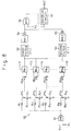
- the sensor of the present embodiment comprises a scanning output generating circuit as shown in FIG 7, incorporating a fail-safe scanning circuit, and a sensor circuit as shown in FIG 8 for detecting the passing of an object.
- the scanning output generating circuit 40 of FIG. 7 comprises first and second fail safe scanning circuits 41, 42 similar to those described in FIG. 1 through FIG. 6, a clock signal generating circuit 43 for supplying a clock signal CK to the scanning circuits 41, 42, a reset signal generating circuit 44 for supplying a reset signal RES to the same scanning circuits 41, 42, and a high frequency generating circuit 45 for supplying a high frequency signal of a frequency f2 to the first fail safe scanning circuit 41.
- a high frequency signal of frequency f1 is only given to the transistors Tr1 through Tr7, while a high frequency signal of frequency f2 is given to the final transistor Tr8 by connecting the output of the high frequency generating circuit 45, in place of the output of the high frequency generating circuit 22, to the input of the AND gate GB8 in the final stage of the second AND gate group 23 of FIG 4.
- the outputs k1, k2 of the fail safe scanning circuits 41, 42 correspond to the output "k" for fault detection in FIG. 6.
- the sensor circuit 50 of FIG. 8 comprises light emitting elements PT1 through PT8, light receiving elements PD1 through PD8, a first filter circuit 52, a second filter circuit 53, main amps MA1, MA2, rectifying circuits 54, 55, an AND gate 56 and an on-delay circuit 57.
- the light emitting elements PT1 through PT8 act as driven objects which are scan driven by the scanning output signals Pi from the before-mentioned first fail-safe scanning circuit 41 via transistors TR1 through TR8.
- the light receiving elements PD1 through PD8 are located opposite the light emitting elements PT1 through PT8, and are connected respectively to the pre-amps PA1 through PA8 driven by application of rectangular wave signals T1 through T8 from the second fail-safe scanning circuit 42, and further sequentially scanned by the pre-amps PA 1 through PA8. They act as driven objects which give an output on receipt of light beams from the light emitting elements PTi.
- the AND gate 51 acts as a fail-safe second logical product operation circuit wherein the output is lost at the time of a failure in a similar manner to that mentioned before, for carrying out the logical product operation on the output k1 from the first fail safe scanning circuit 41 and the power source Vcc.
- the first filter circuit 52 extracts a signal of frequency f1 from the wired OR connected outputs of the output signals from the pre-amps PA1 through PA7.
- the second filter circuit 53 extracts a signal of frequency f2 from the output signal from the final pre-amp PA8.
- the main amps MA1, MA2 amplify the respective outputs from the first filter circuit 52 and second filter circuit 53.
- the rectifying circuits 54, 55 rectify the outputs from the respective main amps MA1, MA2.
- the AND gate 56 acts as a fail safe first logical product operation circuit which carries out, in a similar manner to that mentioned before, a logical product operation on the wired OR output from the rectifying circuits 54, 55, and the output k2 from the second fail-safe scanning circuit 42.
- the on-delay circuit 57 has a construction similar to the on-delay circuit 37 included in the before-mentioned scanning circuit 30, which delays the output for a fixed time to the input from the AND gate 56.
- the first and second fail safe scanning circuits 41, 42 generate periodic synchronous scanning output signals Pi, and rectangular wave signals ti, based on the clock signal CK from the clock signal generating circuit 43, and the reset signal RES from the reset signal generating circuit 44. If the respective scanning circuits 41, 42 are normal, the outputs k1, k2 are input to the respective AND gate 51 and AND gate 56. Consequently, only when the first fail-safe scanning circuit 41 is normal, is a power source voltage Vcc supplied to the light emitting elements PTi.
- the light emitting elements PT1 through PT8 are synchronized with the output of scanning output signals P1 through P7 of frequency f1, and P8 of frequency f2 from the first fail-safe scanning circuit 41, and scanned in a continuous succession along the time axis and emitting light.
- the power supply is input to the pre-amps PA1 through PA8 on the side of the light receiving elements PD in continuous succession along the time axis, on the basis of the rectangular wave signal t1 through t8 from the second fail safe scanning circuit 42.
- the scanning output signals Pi from the first and second fail-safe scanning circuits 41, 42, and the rectangular wave signals ti are normally synchronized, the light beam from the light emitting elements PT1 through PT7 is received by the corresponding light receiving elements PD1 through PD7. It then passes via the corresponding pre-amp PAi, to the first filter 52 where the signal of frequency f1 is filtered. The signal is then amplified by the main amp MA1, and rectified by the rectifying circuit 54. Moreover, the light beam from the light emitting element PT8 is received by the corresponding light receiving element PD8. It then passes via the corresponding pre-amp PA8, to the second filter 52 where the signal of frequency f2 is filtered. The signal is then amplified by the main amp MA2, and rectified by the rectifying circuit 55. Then the wired OR outputs of the rectifying circuits 54, 55, are input to the AND gate 56.
- the delay period of the on-delay circuit 57 is set to be longer than one scanning period, then when the related fault is produced, the output of the on-delay circuit 57 is maintained in the STOP condition (logic value "0"). Furthermore, the circuit can be made so that when the output of the on-delay circuit 57 stops, then switch operation or the like has to be made again to drive the mechanical moving portion of a press etc..
- the frequency of the light for the last light emitting element PT8 is made different to that of the other light emitting elements PT1 through PT7, then when the light emitting element PT8 and the light receiving element PD8 are not synchronized, an output from the main amp MA2 is not generated. It is thus possible to judge whether or not the last light emitting element PT8 is synchronized with the light receiving element PD8 in the one scanning period. Furthermore, with the light beam sensor of the present embodiment, when comprised of a plurality of units connected together as a single unit, the generation of a light received output from the last light receiving element PD8, due to a light beam from a neighboring unit can be prevented.
- FIG. 9 A second embodiment of the multi-axis light beam-type sensor is shown in FIG. 9.
- the light emitting elements PT1 up to PT8 emit light at the same frequency f1.
- the sensor circuit 60 of the second embodiment shown in FIG. 9, has a power source voltage Vcc supplied directly to the light emitting elements PTi. Also the output from the light receiving element PD8, is wired OR connected to the other light receiving elements PD1 through PD7, and input to the f1 filtering filter 57.
- the sensor circuit 60 incorporates the following components.
- An AND gate 62 which acts as a third logical product operation circuit, for carrying out a logical product operation on the rectified output of the scanning output signal P8 from the first fail-safe scanning circuit 41 rectified in the rectifying circuit 61, and the output k1 of the first fail-safe scanning circuit 41.
- a rectifying circuit 63 which rectifies the output from the AND gate 62.
- a capacitor Ca for inputting the rectangular wave signal t8 of the second fail-safe scanning circuit 42 as alternating current.
- An AND gate 64 which acts as a fourth logical product operation circuit for carrying out a logical product operation on the output from the capacitor Ca, and the rectified output from the main amp MA1.
- a rectifying circuit 65 for rectifying the output of the AND gate 64.
- An AND gate 66 which acts as a fifth logical product operation circuit for carrying out a logical product operation on both rectified outputs from the respective rectifying circuits 63 and 65.
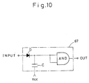
- An off-delay circuit 67 The output from the off-delay circuit 67 is input to the AND gate 56.
- the respective AND gates 62, 64, and 66 have a fail-safe construction such that at the time of a fault, an output is not produced.
- the off-delay circuit 67 is constructed so that at normal times, the output from the AND gate 66 which is generated periodically, is maintained for at least one scanning period. Such an off-delay circuit 67 can be realised if a diode D and capacitor C are inserted on the input side of the fail-safe AND gate as shown in FIG. 10.
- the output from the off-delay circuit 67 becomes a logical value of "1" only when the light emitting element PT8 and the light receiving element PD8 are synchronized. If all is normal, an output is generated from the AND gate 56, generating an output from the on-delay circuit 57 which indicates that the sensor circuit 60 is normal.
- the present invention used in a system operating in a work space common to both a machine and an operator, the safety of the operator working in the common work space can be considerably improved. Hence operator injury from the machine can be prevented, greatly improving industrial utility.
Landscapes
- Physics & Mathematics (AREA)
- Nonlinear Science (AREA)
- Photometry And Measurement Of Optical Pulse Characteristics (AREA)
- Length Measuring Devices By Optical Means (AREA)
- Electronic Switches (AREA)
Abstract
Applications Claiming Priority (1)
| Application Number | Priority Date | Filing Date | Title |
|---|---|---|---|
| PCT/JP1992/000631 WO1993023772A1 (fr) | 1992-05-15 | 1992-05-15 | Circuit a balayage a surete intrinseque et capteur du type a faisceaux a axes optique multiples |
Publications (3)
| Publication Number | Publication Date |
|---|---|
| EP0594852A1 true EP0594852A1 (fr) | 1994-05-04 |
| EP0594852A4 EP0594852A4 (en) | 1995-12-27 |
| EP0594852B1 EP0594852B1 (fr) | 1998-08-05 |
Family
ID=14042344
Family Applications (1)
| Application Number | Title | Priority Date | Filing Date |
|---|---|---|---|
| EP92909797A Expired - Lifetime EP0594852B1 (fr) | 1992-05-15 | 1992-05-15 | Circuit a balayage a surete intrinseque et capteur du type a faisceaux a axes optique multiples |
Country Status (4)
| Country | Link |
|---|---|
| US (1) | US5432337A (fr) |
| EP (1) | EP0594852B1 (fr) |
| DE (1) | DE69226529T2 (fr) |
| WO (1) | WO1993023772A1 (fr) |
Families Citing this family (8)
| Publication number | Priority date | Publication date | Assignee | Title |
|---|---|---|---|---|
| US5442303A (en) * | 1992-07-16 | 1995-08-15 | The Nippon Signal Co., Ltd. | Electromagnetically coupled fail-safe logic circuit |
| EP0825458B1 (fr) | 1996-03-08 | 2002-10-30 | Nihon Shingo Kabushiki Kaisha | Barriere optique |
| EP0867274A1 (fr) * | 1996-09-03 | 1998-09-30 | The Nippon Signal Co. Ltd. | Appareil permettant d'agir automatiquement sur le fonctionnement du coulisseau d'une presse a securite integree |
| JPH1190696A (ja) | 1997-09-19 | 1999-04-06 | Nippon Signal Co Ltd:The | プレス機械の運転装置 |
| JP4141039B2 (ja) | 1998-06-10 | 2008-08-27 | 日本信号株式会社 | 閾値演算回路及びこれを用いたandゲート回路、自己保持回路及び起動信号発生回路 |
| JP4442272B2 (ja) * | 2004-03-22 | 2010-03-31 | 富士ゼロックス株式会社 | 画像読み取り装置、基準部材の異物検知方法 |
| US7748815B2 (en) | 2007-08-06 | 2010-07-06 | Hewlett-Packard Development Company, L.P. | Disabling a nozzle |
| US7810697B2 (en) * | 2008-08-22 | 2010-10-12 | Honda Motor Co., Ltd. | Turntable welding system with light curtain protection |
Family Cites Families (11)
| Publication number | Priority date | Publication date | Assignee | Title |
|---|---|---|---|---|
| US3805061A (en) * | 1973-04-23 | 1974-04-16 | Tyco Laboratories Inc | Object detecting apparatus |
| US4309696A (en) * | 1978-06-26 | 1982-01-05 | Kabushiki Kaisha Komatsu Seisakusho | Trouble detecting unit in an optical security device |
| US4266124A (en) * | 1979-08-10 | 1981-05-05 | Data Instruments, Inc. | Photoelectric object detector system |
| US4520262A (en) * | 1979-09-10 | 1985-05-28 | Kenneth Ambler | Photoelectric safety screen with stray source detection |
| JPS5698667A (en) * | 1980-01-10 | 1981-08-08 | Fuji Electric Co Ltd | Object detector |
| JPS57142578A (en) * | 1981-02-28 | 1982-09-03 | Riken Lens Kogyo Kk | Automatic check device for light beam type safety device |
| JPH0669274B2 (ja) * | 1984-04-19 | 1994-08-31 | 日本信号株式会社 | 負荷駆動用スイッチ回路の監視装置 |
| JPS60227326A (ja) * | 1984-04-25 | 1985-11-12 | 日本信号株式会社 | 負荷駆動用スイツチ回路の監視装置 |
| DE3601516A1 (de) * | 1986-01-20 | 1987-07-23 | Agie Ag Ind Elektronik | Lichtschranke |
| US5015840B1 (en) * | 1990-01-09 | 1995-04-11 | Scient Technologies Inc | Self-checking light curtain system and method of operation. |
| US5218196A (en) * | 1991-09-05 | 1993-06-08 | Frost Controls, Inc. | Light curtain system with system and watchdog microcontrollers |
-
1992
- 1992-05-15 US US08/175,398 patent/US5432337A/en not_active Expired - Fee Related
- 1992-05-15 WO PCT/JP1992/000631 patent/WO1993023772A1/fr not_active Ceased
- 1992-05-15 DE DE69226529T patent/DE69226529T2/de not_active Expired - Fee Related
- 1992-05-15 EP EP92909797A patent/EP0594852B1/fr not_active Expired - Lifetime
Also Published As
| Publication number | Publication date |
|---|---|
| US5432337A (en) | 1995-07-11 |
| WO1993023772A1 (fr) | 1993-11-25 |
| EP0594852B1 (fr) | 1998-08-05 |
| EP0594852A4 (en) | 1995-12-27 |
| DE69226529T2 (de) | 1999-01-21 |
| DE69226529D1 (de) | 1998-09-10 |
Similar Documents
| Publication | Publication Date | Title |
|---|---|---|
| US4266124A (en) | Photoelectric object detector system | |
| EP0594852B1 (fr) | Circuit a balayage a surete intrinseque et capteur du type a faisceaux a axes optique multiples | |
| US4309696A (en) | Trouble detecting unit in an optical security device | |
| US20220100163A1 (en) | Configurable safety module for detecting digital or analog input or output signals | |
| US4215340A (en) | Process for the automatic signalling of faults of a static automatic module and a module for realizing the process | |
| US5495228A (en) | Fail-safe scan circuit and a multibeam sensor | |
| US9083946B2 (en) | System to detect failed pixels in a sensor array | |
| US6922904B2 (en) | Method and system for analyzing transmitted signals from a probe system | |
| US5640006A (en) | Control circuit for a fail-safe multi-axis light beam type sensor | |
| JPWO1995010789A1 (ja) | フェールセーフ多光軸光線式センサ | |
| US9768212B2 (en) | Method and apparatus for enabling sensors in a dual matrix sensor array | |
| US20190180957A1 (en) | Switch device including dual on/off signal generation units, and numerical control system | |
| JPWO1993023772A1 (ja) | フェールセーフ走査回路及び多光軸光線式センサ | |
| US6163164A (en) | Noise detection circuit | |
| US4574343A (en) | Contactless press control device | |
| KR102352129B1 (ko) | 이상 신호 방지 장치 | |
| SE416754B (sv) | Sekerhetsanordning for en press | |
| JPH11259101A (ja) | フェールセーフ出力装置 | |
| JPS6235930A (ja) | クロツク診断方式 | |
| SU834616A1 (ru) | Устройство дл контрол релейнойКОММуТАциОННОй элЕКТРОАппАРАТуРы | |
| SU779141A1 (ru) | Система контрол состо ни путевых устройств электрической централизации и автоблокировки | |
| SU520286A1 (ru) | Устройство электрической централизации стрелок и сигналов | |
| SU1231479A1 (ru) | Способ контрол логических микросхем | |
| SU736256A1 (ru) | Реле сопротивлени | |
| CN119764205A (zh) | 一种硅片的破片检测装置及方法 |
Legal Events
| Date | Code | Title | Description |
|---|---|---|---|
| PUAI | Public reference made under article 153(3) epc to a published international application that has entered the european phase |
Free format text: ORIGINAL CODE: 0009012 |
|
| 17P | Request for examination filed |
Effective date: 19940112 |
|
| AK | Designated contracting states |
Kind code of ref document: A1 Designated state(s): DE FR GB |
|
| A4 | Supplementary search report drawn up and despatched | ||
| AK | Designated contracting states |
Kind code of ref document: A4 Designated state(s): DE FR GB |
|
| 17Q | First examination report despatched |
Effective date: 19960328 |
|
| GRAG | Despatch of communication of intention to grant |
Free format text: ORIGINAL CODE: EPIDOS AGRA |
|
| GRAG | Despatch of communication of intention to grant |
Free format text: ORIGINAL CODE: EPIDOS AGRA |
|
| GRAH | Despatch of communication of intention to grant a patent |
Free format text: ORIGINAL CODE: EPIDOS IGRA |
|
| GRAH | Despatch of communication of intention to grant a patent |
Free format text: ORIGINAL CODE: EPIDOS IGRA |
|
| GRAA | (expected) grant |
Free format text: ORIGINAL CODE: 0009210 |
|
| AK | Designated contracting states |
Kind code of ref document: B1 Designated state(s): DE FR GB |
|
| REF | Corresponds to: |
Ref document number: 69226529 Country of ref document: DE Date of ref document: 19980910 |
|
| ET | Fr: translation filed | ||
| PLBE | No opposition filed within time limit |
Free format text: ORIGINAL CODE: 0009261 |
|
| 26N | No opposition filed | ||
| REG | Reference to a national code |
Ref country code: GB Ref legal event code: IF02 |
|
| PGFP | Annual fee paid to national office [announced via postgrant information from national office to epo] |
Ref country code: GB Payment date: 20020515 Year of fee payment: 11 |
|
| PGFP | Annual fee paid to national office [announced via postgrant information from national office to epo] |
Ref country code: DE Payment date: 20020528 Year of fee payment: 11 |
|
| PGFP | Annual fee paid to national office [announced via postgrant information from national office to epo] |
Ref country code: FR Payment date: 20020531 Year of fee payment: 11 |
|
| PG25 | Lapsed in a contracting state [announced via postgrant information from national office to epo] |
Ref country code: GB Free format text: LAPSE BECAUSE OF NON-PAYMENT OF DUE FEES Effective date: 20030515 |
|
| PG25 | Lapsed in a contracting state [announced via postgrant information from national office to epo] |
Ref country code: DE Free format text: LAPSE BECAUSE OF NON-PAYMENT OF DUE FEES Effective date: 20031202 |
|
| GBPC | Gb: european patent ceased through non-payment of renewal fee |
Effective date: 20030515 |
|
| PG25 | Lapsed in a contracting state [announced via postgrant information from national office to epo] |
Ref country code: FR Free format text: LAPSE BECAUSE OF NON-PAYMENT OF DUE FEES Effective date: 20040130 |
|
| REG | Reference to a national code |
Ref country code: FR Ref legal event code: ST |