EP0594906B1 - Circuit de commande pour moteur universel série (ou compound) - Google Patents
Circuit de commande pour moteur universel série (ou compound) Download PDFInfo
- Publication number
- EP0594906B1 EP0594906B1 EP92309852A EP92309852A EP0594906B1 EP 0594906 B1 EP0594906 B1 EP 0594906B1 EP 92309852 A EP92309852 A EP 92309852A EP 92309852 A EP92309852 A EP 92309852A EP 0594906 B1 EP0594906 B1 EP 0594906B1
- Authority
- EP
- European Patent Office
- Prior art keywords
- circuit
- resistor
- voltage
- field winding
- series
- Prior art date
- Legal status (The legal status is an assumption and is not a legal conclusion. Google has not performed a legal analysis and makes no representation as to the accuracy of the status listed.)
- Expired - Lifetime
Links
Images


Classifications
-
- H—ELECTRICITY
- H02—GENERATION; CONVERSION OR DISTRIBUTION OF ELECTRIC POWER
- H02P—CONTROL OR REGULATION OF ELECTRIC MOTORS, ELECTRIC GENERATORS OR DYNAMO-ELECTRIC CONVERTERS; CONTROLLING TRANSFORMERS, REACTORS OR CHOKE COILS
- H02P25/00—Arrangements or methods for the control of AC motors characterised by the kind of AC motor or by structural details
- H02P25/02—Arrangements or methods for the control of AC motors characterised by the kind of AC motor or by structural details characterised by the kind of motor
- H02P25/10—Commutator motors, e.g. repulsion motors
- H02P25/14—Universal motors
Definitions
- the present invention relates to universal type series (or compound) motors, and more particularly, to a device for governing the auxiliary field winding's intensity of such motors.
- the present invention provides a governor circuit for limiting the top speed of a universal series or compound motor of the type having a series-connected main field winding and an armature, the governor circuit comprising a voltage detector circuit coupled to the armature of the motor for detecting a threshold voltage across the armature, a current shunting circuit connected to the voltage detector circuit and triggered thereby upon detection of the threshold voltage to shunt current around the armature, characterised in that an auxiliary field winding is coupled across the armature for providing a current shunt path around the armature, the current shunting circuit being connected in series with the auxiliary field winding for selectively shunting current therethrough upon the voltage detector circuit detecting the threshold voltage, whereby the armature voltage is clamped at the threshold level and the motor is limited to a maximum speed in accordance therewith.
- the current shunting circuit is triggered when the armature voltage reaches the threshold to shunt current away from the armature, thereby limiting the speed of the motor.
- the governor circuit will detect the armature voltage of the series (or compound) motor, and additionally trigger the current shunting circuit when the armature voltage reaches the preset threshold to shunt current through the auxiliary field winding as needed.
- An amplifier circuit may be provided to increase the reaction time of the governor circuit.
- the governor circuit may be varied to accommodate the various conventional power supply types.
- the components of the governor circuit may be variable to allow adjustment of the voltage threshold.
- a conventional isolator circuit such as an optoisolator, may be interconnected between the voltage detector circuit and the current shunting circuit to electrically isolate the two circuits.
- a conventional amplifier-coupler may be interconnected between the voltage detector circuit and the current shunting circuit to expedite transmission of the trigger signal between the two circuits.
- the present invention eliminates the above-described drawbacks by governing the field intensity of such motors.
- FIG. 1 is a block diagram configuration of the governor circuit according to one embodiment of the present invention.
- the governor circuit is shown to be incorporated in a conventional series motor, wherein a field winding F1 and an armature A1 are connected in series.
- the governor circuit includes and auxiliary field winding F101 in series with a current shunting element 101, both conhected in parallel across the armature A1 of the series motor.
- the current shunting element 101 may be any voltage-triggered switch device capable of selectively gating current through to the auxiliary field winding F101.
- a voltage detector element 102 is connected in parallel with the armature A1 across the series-connected field winding F101 and current shunting element 101.
- the voltage detector 102 simply detects when the armature A1 voltage exceeds a predetermined threshold, and this may be done by conventional voltage division.
- voltage detector 102 triggers the current shunting element 101 to shunt current through the auxiliary field winding F101 and around the armature A1.
- the current shunting element 101 is preferably a conventional AC switching device such as a triac, or alternatively, a full bridge rectifier in conjunction with a uni-directional switching device such as a silicon controlled rectifier or power transistor.
- triac is considered to be a common term of art and is intended to designate the equivalent of parallely-connected silicon controlled rectifiers which serve as a gated AC control switch.
- Voltage detector 102 is preferably a conventional voltage-divider network which may include a bridge-type rectifier.
- the governor circuit may be powered by pulsed-DC, in which case the current shunting element 101 may be a conventional uni-directional switching device such as a thyristor or power transistor.
- the governor circuit may also be DC powered, in which case the current shunting element 101 is preferably a power transistor.
- the above-described governor circuit provides a top-speed limiting function.
- the speed will accelerate and the voltage appearing across the armature A1 will increase accordingly.
- Voltage detector 102 will detect the predetermined armature A1 threshold voltage level and will thereupon trigger the current shunting circuit 101.
- Current shunting circuit 101 will conduct, thereby shunting current through the auxiliary field winding F101. This shunting action clamps the armature A1 voltage to the preset threshold voltage level and limits the speed of the motor in accordance with the threshold level.
- the speed governor function is very useful in light-load/high-speed conditions, when the speed of the motor can reach harmfully high levels.
- the voltage detector circuit 102 may be made adjustable in order that the threshold voltage level may be varied. This way, the top speed limit of the motor can be varied as well.
- FIG. 2 is a block diagram of an alternative embodiment of the governor circuit according to the present invention.
- a series-connected current shunting element 101 and auxiliary field winding F101 are placed in parallel with the main field winding F1.
- a voltage detector 102 is connected in parallel with the armature A1 in order to detect the armature voltage.
- the voltage detecting and current shunting functions are essentially the same as described in FIG. 1, however, when the voltage detecting circuit 102 triggers the current shunting circuit 101 to conduct, current is shunted through the auxiliary field winding F101 around the main field winding F1. This shunting action clamps the main field winding F1 voltage to the preset threshold voltage level and limits the speed of the motor in accordance with the threshold level.
- FIG. 3 is a block diagram of a third embodiment of the governor circuit in accordance with the present invention.
- the series-connected current shunting element 101 and auxiliary field winding F101 are connected in parallel with the series combination of the main field winding F1 and the armature A1.
- the voltage detector 102 is connected in parallel with the armature A1.
- the voltage detecting and current shunting functions are essentially the same as described in regard to FIG. 1, however, when the voltage detecting circuit 102 triggers the current shunting circuit 101 to conduct, current is shunted through the auxiliary field winding F101 around both the main field winding F1 and armature A1. This shunting action clamps the combined voltage across both the main field winding F1 and armature A1 to the preset threshold voltage level and limits the speed of the motor in accordance with the threshold level.
- FIG. 4 is a block diagram of the governor circuit according to the present invention further including a conventional isolator-type coupling interface 104 which is interconnected between the voltage detector 102 and the current shunting element 101.
- the coupling interface 104 may take the form of a photoelectric or optical-isolator type coupler or a solenoid coupler. This coupler may be employed in any of the three governor circuit embodiments described in FIGS. 1-3.
- FIGS. 5-11 depict detailed schematics of several possible embodiments of the governor circuit which are designed to accommodate AC, DC, or pulsed-DC power supply types.
- FIG. 5 illustrates a governor circuit employing a triac TRIAC1 as the current shunt element 101, TRIAC1 being connected in series with the auxiliary field winding F101, and a series resistor-divider pair, R1 and R2, as the voltage detecting element 102, resistors R1 and R2 being connected in parallel with TRIAC1 and auxiliary winding F101.
- two bi-polar Zener diodes ZD1 and ZD2 are connected in series to couple the gate of TRIAC1 with the voltage divided level established between resistors R1 and R2.
- This governor circuit may be used in conjunction with AC or pulsed-DC power supply types.
- Resistor R1 of the voltage detector 102 may be a variable resistor or a stepwise adjustable resistor to allow adjustment of the threshold voltage level and resulting top speed of the motor.
- FIG. 6 is another embodiment of the governor circuit in which the Zener diodes ZD1, ZD2 of FIG. 5 are replaced by an AC diode DIAC1.
- diac is considered to be a common term of art and is intended to designate the equivalent of an AC diode, which essentially serves the same purpose as two bi-polar diodes.
- resistor R2 is replaced by a capacitor C1 to form an R-C voltage divider which serves as voltage detector 102.
- This circuit may be used in conjunction with AC power supply types.
- resistor R1 of the voltage detector may be replaced by a variable or stepwise resistor, and similarly, capacitor C1 may be replaced by a variable or stepwise capacitor to allow modification of the threshold voltage level and top speed of the motor.
- FIG. 7 is another embodiment of the governor circuit which employs a full bridge-type rectifier including diodes D1-D4.
- a silicon controlled rectifier SCR1 is coupled in series with the auxiliary field winding F101 across the diode bridge to form the current shunt element 101, and a series resistor pair R1 and R2 are coupled across the diode bridge to form the detector element 102.
- the anode A of SCR1 is connected to the positive end of the diode bridge rectifier circuit, while cathode K of SCR1 is connected to the negative end of the diode bridge rectifier circuit.
- the voltage divided level between resistors R1 and R2 is connected to the gate G of SCR1 through a protective diode D201, and a protective shunt resistor R201 may be connected across gate (G) and cathode (K) of the SCR1.
- Rectifier D1-D4 allows uni-directional current flow when coupled to an AC source, and this facilitates the use of the uni-directional switch SCR1.
- Protective diode D201 prevents the backflow of AC current to the series resistors R1 and R2.
- This governor circuit may be used with AC or pulsed-DC power supply types.
- resistor R1 may be a variable or stepwise resistor to allow modification of the threshold voltage level and the top speed limit of the motor.
- FIG. 8 is a variation of the embodiment in FIG. 7 which is suited for use with AC and pulsed-DC power supply types.
- resistor R2 of the FIG. 7 is replaced by capacitor C1
- protective diode D201 and protective resistor R201 of FIG. 7 are replaced by a trigger diode DIAC1.
- the operation of the governor circuit of FIG. 8 is essentially as described in regard to FIG. 6, however, no rectification is provided.
- FIG. 9 is a schematic of another embodiment of the governor circuit which employs a silicon controlled rectifier SCR1 as the shunt element 101 and a series resistor pair R1 and R2 as the detector element 102.
- the anode A of SCR1 is connected in series to the auxiliary field winding F101, and series-connected SCR1 and F101 are connected in parallel across the series resistors R1 and R2.
- the gate G of SCR1 is coupled to the divided voltage between resistors R1 and R2 via protective diode D201.
- a resistor R201 is connected between the auxiliary field winding F101 and the gate G of SCR1.
- the operation of the governor circuit of FIG. 9 is essentially as described in regard to FIG. 7, however, no rectification is provided.
- This governor circuit is suitable for use with a pulsed-DC power supply.
- Resistor R1 may be replaced by a variable or stepwise resistor to allow modification of the threshold voltage level and top speed of the motor.
- FIG. 10 is a schematic diagram of another alternative embodiment of the governor circuit which employs a full bridge-type rectifier including diodes D1-D4, and a power transistor Q1 connected in series with auxiliary winding F101 to form the shunt element 101, the collector C of transistor Q1 being coupled to the positive end of the diode bridge, and the emitter E being coupled to the negative end.
- a series-resistor pair R1 and R2 are also coupled across the diode bridge to form the voltage detector 102.
- the base B of power transistor Q1 is directly coupled to the divided voltage level between resistors R1 and R2 of the voltage detector 102.
- the operation of the governor circuit of FIG. 10 is essentially as described in regard to FIG. 7. This governor circuit is suited for use with an AC, DC, or pulsed-DC power supply types.
- Resistor R1 may be a variable or stepwise adjustable resistor to allow modification of the threshold voltage level and top speed of the motor.
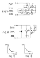
- FIG. 11 is a schematic of another embodiment of the governor circuit which employs a power transistor Q1 as the current shunt element 101 connected in series with the auxiliary winding F101, and a series resistor pair R1 and R2 as the detector element 102.
- the shunt element Q1 and the auxiliary field winding F101 are connected in parallel with the series resistors R1 and R2, which are in turn connected in parallel with a flywheel diode D8.
- the collector C is connected to terminal a for connection to the positive end of the armature, and the emitter E is connected to terminal b for connection to the negative end of the armature.
- the collector C should be connected to the negative end of the armature while the emitter E should be connected to the positive end of the armature.
- the base B of power transistor Q1 is directly coupled with the divided voltage level at the series connection between resistors R1 and R2 of the detector element 102.
- the operation of the governor circuit of FIG. 11 is essentially as described in regard to FIG. 10, however, no rectification is provided.
- This governor circuit may be used with DC or pulsed-DC power supply types.
- Resistor R1 may be a variable or stepwise adjustable resistor to allow modification of the threshold voltage level and top speed of the motor.
- a conventional isolator-type coupling interface 104 as shown in FIG. 4 may be interconnected between the voltage detector 102 and the current shunting element 101 to isolate the two.
- the coupling interface 104 may be a photoelectric or optical-isolator type coupler or a solenoid coupler.
- reaction time between voltage threshold level detection at voltage detector 102 and clamping of motor speed by current shunt element 101 can be reduced in all of the above-described embodiments of FIGs. 5-11 simply by connecting a conventional amplifier circuit between the detector and shunt elements.
- a conventional amplifier circuit may take the form of a Darlington power transistor or a thyristor.
- any of the passive components such as resistors R1 and R2, capacitor C1, etc., may be a variable or stepwise adjustable component to allow modification of the threshold voltage level and top speed of the motor.
- FIG. 12 is a graph of the RPM (speed) v. TORQUE (load) characteristics of a conventional series motor under normal operating conditions. Note that with decreasing load the motor speed increases rapidly. This may have harmful consequences under light-load conditions.
- FIG. 13 is a RPM (speed) v. TORQUE (load) graph of the RPM (speed) v. TORQUE (load) characteristics of a conventional series motor employing a governor circuit in accordance with the present invention.
- the top speed of the motor is clamped at a preset limit by the governor. This top speed limit is directly related to the threshold voltage level as determined by the voltage detector 102. Once the threshold voltage level is detected at voltage detector 102, the current shunting element 101 is triggered, and this diverts current from the armature A1, thereby clamping the armature A1 voltage at the threshold level and limiting the top speed of the motor.
Landscapes
- Engineering & Computer Science (AREA)
- Power Engineering (AREA)
- Control Of Direct Current Motors (AREA)
- Control Of Eletrric Generators (AREA)
Claims (34)
- Circuit de commande pour limiter la vitesse supérieure d'un moteur universel série ou compound du type comportant un enroulement de champ principal (F1) et un induit (A1) branchés en série, le circuit de commande comprenant un circuit détecteur de tension (102) couplé à l'induit du moteur pour détecter une tension de seuil aux bornes de cet induit, un circuit de shuntage de courant (101) branché au circuit détecteur de tension et déclenché par celui-ci, au moment de la détection de la tension de seuil, pour shunter le courant en contournant l'induit,
caractérisé en ce que
un enroulement de champ auxiliaire (F101) est couplé aux bornes de l'induit pour fournir un chemin de shuntage de courant contournant cet induit, le circuit de shuntage de courant étant branché en série avec l'enroulement de champ auxiliaire pour shunter sélectivement le courant à travers celui-ci lorsque le circuit détecteur de tension détecte la tension de seuil, ce qui permet ainsi de bloquer la tension de l'induit au niveau de seuil, et de limiter en conséquence la vitesse maximum du moteur. - Circuit de commande selon la revendication 1,
dans lequel
le circuit détecteur de tension (102) est branché en parallèle avec le circuit série constitué de l'enroulement de champ auxiliaire (F101) et du circuit de shuntage de courant (101), et se trouve également branché en parallèle avec l'induit (A1). - Circuit de commande selon la revendication 2,
dans lequel
le circuit détecteur de tension (102) comporte en outre un diviseur de tension comprenant une première résistance (R1) et une seconde résistance (R2) branchées en série pour fournir une tension de référence divisée entre elles, et le circuit de shuntage de courant (101) comprend en outre un triac (TRIAC1) dont la grille est branchée entre la première et la seconde résistance par une paire bipolaire de diodes Zener (ZD1, ZD2) pour commander le passage du courant en fonction de la tension de référence. - Circuit de commande selon la revendication 3
dans lequel
la première résistance (R1) est une résistance variable pour permettre le réglage de la référence de tension divisée. - Circuit de commande selon la revendication 3,
dans lequel
la seconde résistance (R2) est une résistance variable pour permettre le réglage de la référence de tension divisée. - Circuit de commande selon la revendication 2,
dans lequel
le circuit détecteur de tension (102) comporte en outre un diviseur de tension comprenant une résistance (R1) et un condensateur (C1) branchés en série pour fournir une tension de référence entre eux, et le circuit de shuntage de courant (101) comprend en outre un triac (TRIAC1) et un diac (DIAC1), la grille du triac étant branchée entre la résistance et le condensateur par l'intermédiaire du diac, pour commander le passage du courant en fonction de la tension de référence. - Circuit de commande selon la revendication 6,
dans lequel
la résistance (R1) est une résistance variable pour permettre le réglage de la référence de tension divisée. - Circuit de commande selon la revendication 6,
dans lequel
le condensateur (C1) est un condensateur variable pour permettre le réglage de la référence de tension divisée. - Circuit de commande selon la revendication 2,
dans lequel,
le circuit détecteur de tension (102) comporte en outre un diviseur de tension comprenant une première résistance (R1) et une seconde résistance (R2) branchées en série pour fournir une tension de référence divisée entre elles, et le circuit de shuntage de courant (101) comprend en outre un redresseur commandé au silicium (SCR1) et une diode (D201), la grille du redresseur commandé au silicium étant branchée entre la première et la seconde résistance par l'intermédiaire de la diode, pour commander le passage du courant en fonction de la tension de référence. - Circuit de commande selon la revendication 9,
dans lequel
la première résistance (R1) est une résistance variable pour permettre le réglage de la référence de tension divisée. - Circuit de commande selon la revendication 9,
dans lequel
la seconde résistance (R2) est une résistance variable pour permettre le réglage de la référence de tension divisée. - Circuit de commande selon la revendication 9,
dans lequel
le circuit de shuntage de courant (101) comprend en outre une résistance de protection (R201) branchée entre la grille du redresseur commandé au silicium (SCR1) et l'enroulement de champ auxiliaire (F101). - Circuit de commande selon la revendication 2,
dans lequel,
le circuit détecteur de tension (102) comporte en outre un diviseur de tension comprenant une première résistance (R1) et une seconde résistance (R2) branchées en série pour fournir une tension de référence divisée entre elles, et le circuit de shuntage de courant (101) comprend en outre un transistor (Q1) dont le collecteur et l'émetteur sont branchés en série avec l'enroulement de champ auxiliaire (F101), la base de ce transistor étant en outre branchée entre la première et la seconde résistance pour commander le passage du courant en fonction de la tension de référence. - Circuit de commande selon la revendication 13,
comprenant en outre
une diode (D8) branchée en parallèle aux bornes du circuit série constitué du transistor (Q1) et de l'enroulement de champ auxiliaire (F101). - Circuit de commande selon la revendication 13,
dans lequel
la première résistance (R1) est une résistance variable pour permettre le réglage de la référence de tension divisée. - Circuit de commande selon la revendication 13,
dans lequel
la seconde résistance (R2) est une résistance variable pour permettre le réglage de la référence de tension divisée. - Circuit de commande selon la revendication 1,
dans lequel
l'enroulement de champ auxiliaire (F101) et le circuit de shuntage de courant (101) sont branchés en parallèle sur l'enroulement de champ principal (F1) du moteur, le circuit détecteur de tension (102) est branché en parallèle sur l'induit (A1) du moteur, et le circuit détecteur de tension (102) est branché en série avec l'enroulement de champ auxiliaire (F101) et le circuit de shuntage de courant (101). - Circuit de commande selon la revendication 1,
dans lequel
le circuit détecteur de tension est branché en parallèle avec l'armature (A1) du moteur, tandis que l'enroulement de champ auxiliaire (F101) et le circuit de shuntage de courant (101) sont branchés en parallèle avec l'induit (A1) et l'enroulement de champ principal (F1) du moteur. - Circuit de commande selon la revendication 1,
dans lequel
le circuit détecteur de tension est branché (102) comprend en outre quatre diodes (D1-D4) branchées dans une configuration en pont complet, une première résistance (R1) et une seconde résistance (R2) branchées en série et couplées aux bornes du pont de diodes pour fournir une tension de référence divisée entre elles, et le circuit de shuntage de courant (101) comprend en outre un redresseur commandé au silicium (SCR1) branché en série avec l'enroulement de champ auxiliaire (F101) et le pont de diodes, ainsi qu'une diode (D201) reliant la grille du redresseur commandé au silicium, au branchement série formé entre la première résistance (R1) et la seconde résistance (R2), le redresseur commandé au silicium étant ainsi déclenché en fonction de la tension de référence pour shunter le courant à travers l'enroulement de champ auxiliaire. - Circuit de commande selon la revendication 19,
dans lequel
le circuit de shuntage de courant comprend en outre une résistance de protection (R201) branchée entre la grille du redresseur commandé au silicium (SCR1) et l'enroulement de champ auxiliaire (F101). - Circuit de commande selon la revendication 1,
dans lequel
le circuit détecteur de tension (102) comprend en outre quatre diodes (D1- D4) branchées dans une configuration en pont complet, ainsi qu'une résistance (R1) et un condensateur (C1) branchés en série et couplés aux bornes du pont de diodes pour fournir une tension de référence entre eux, et le circuit de shuntage de courant (101) comprend en outre un redresseur commandé au silicium (SCR1) branché en série avec l'enroulement de champ auxiliaire (F101) et aux bornes du pont de diodes, ainsi qu'un diac (DIAC1) reliant la grille du redresseur commandé au silicium, au branchement série entre la résistance (R1) et le condensateur (C1), le redresseur commandé au silicium étant ainsi déclenché en fonction de la tension de référence pour shunter le courant à travers l'enroulement de champ auxiliaire. - Circuit de commande selon la revendication 21,
dans lequel
la résistance (R1) est une résistance variable pour permettre le réglage de la référence de tension divisée. - Circuit de commande selon la revendication 21,
dans lequel
le condensateur (C1) est un condensateur variable pour permettre le réglage de la référence de tension divisée. - Circuit de commande selon la revendication 1,
dans lequel
le circuit détecteur de tension (102) comprend en outre quatre diodes (D1-D4) branchées dans une configuration en pont complet, une première résistance (R1) et une seconde résistance (R2) branchées en série et couplées aux bornes du pont de diodes pour fournir une tension de référence entre elles, et le circuit de shuntage de courant (101) comprend en outre un transistor (Q1) dont le collecteur (C) et l'émetteur (E) sont branchés en série avec l'enroulement de champ auxiliaire (F101) et aux bornes du pont de diodes, le transistor comportant en outre une base (B) branchée entre la première et la seconde résistance, ce transistor étant ainsi déclenché en fonction de la tension de référence pour shunter le courant à travers l'enroulement de champ auxiliaire. - Circuit de commande selon la revendication 24,
dans lequel
la première résistance (R1) est une résistance variable pour permettre le réglage de la référence de tension divisée. - Circuit de commande selon la revendication 24,
dans lequel
la seconde résistance (R2) est une résistance variable pour permettre le réglage de la référence de tension divisée. - Circuit de commande selon la revendication 1,
comprenant en outre
un circuit isolateur (104) branchée entre le circuit de shuntage de courant (101) et le circuit détecteur de tension (102) pour fournir un couplage isolé électriquement entre les deux, le circuit de shuntage de courant étant déclenché par le circuit détecteur de tension par l'intermédiaire du circuit isolateur lorsque la tension de seuil est détectée, pour shunter le courant à travers l'enroulement de champ auxiliaire (F101). - Circuit de commande selon la revendication 27,
dans lequel
le circuit détecteur de tension (102) est branché en parallèle avec l'enroulement de champ auxiliaire (F101) et le circuit de shuntage de courant (101), en étant en outre branché en parallèle sur l'induit (A1). - Circuit de commande selon la revendication 27,
dans lequel
l'enroulement de champ auxiliaire (F101) et le circuit de shuntage de courant (101) sont branchés en parallèle sur l'enroulement de champ principal (F1), le circuit détecteur de tension (102) est branché en parallèle sur l'induit (A1), et le circuit détecteur de tension est branché en série avec l'enroulement de champ auxiliaire (F101) et le circuit de shuntage de courant (101). - Circuit de commande selon la revendication 27,
dans lequel
le circuit détecteur de tension (102) est branché en parallèle avec l'armature (A1), tandis que l'enroulement de champ auxiliaire (F101) et le circuit de shuntage de courant (101) sont branchés en parallèle avec l'induit et l'enroulement de champ principal (F1). - Circuit de commande selon la revendication 1,
comprenant en outre
un circuit amplificateur branché entre le circuit de shuntage de courant (101) et le circuit détecteur de tension (102) pour activer la transmission d'un signal de déclenchement entre les deux, le circuit de shuntage de courant étant déclenché par le circuit détecteur de tension par l'intermédiaire du circuit amplificateur lorsque la tension de seuil est détectée, pour shunter le courant à travers l'enroulement de champ auxiliaire (F101). - Circuit de commande selon la revendication 31,
dans lequel
le circuit détecteur de tension (101) est branché en parallèle avec l'enroulement de champ auxiliaire (F101) et le circuit de shuntage de courant (101), en étant en outre branché en parallèle sur l'induit (A1). - Circuit de commande selon la revendication 31,
dans lequel
l'enroulement de champ auxiliaire (F101) et le circuit de shuntage de courant (101) sont branchés en parallèle avec l'enroulement de champ principal (F1), le circuit détecteur de tension (102) est branché en parallèle avec l'induit (A1), et le circuit détecteur de tension est branché en série avec l'enroulement de champ auxiliaire (F101) et le circuit de shuntage de courant. - Circuit de commande selon la revendication 31,
dans lequel
le circuit détecteur de tension (102) est branché en parallèle avec l'induit (A1), tandis que l'enroulement de champ auxiliaire (F101) et le circuit de shuntage de courant (101), sont branchés en parallèle avec l'induit (A1) et l'enroulement de champ principal (F1).
Priority Applications (5)
| Application Number | Priority Date | Filing Date | Title |
|---|---|---|---|
| DK92309852.9T DK0594906T3 (da) | 1992-10-28 | 1992-10-28 | Styrekredsløb til serie- (eller compound) motorer af universaltypen |
| ES92309852T ES2101811T3 (es) | 1992-10-28 | 1992-10-28 | Circuito regulador para motor universal en serie (o compound). |
| DE69217949T DE69217949T2 (de) | 1992-10-28 | 1992-10-28 | Regelungskreis für einen universellen Reihenschluss- (oder Kompoundmotor |
| EP92309852A EP0594906B1 (fr) | 1992-10-28 | 1992-10-28 | Circuit de commande pour moteur universel série (ou compound) |
| US08/006,473 US5399948A (en) | 1991-08-14 | 1993-01-21 | Governor circuit for universal series (or compound) motor |
Applications Claiming Priority (2)
| Application Number | Priority Date | Filing Date | Title |
|---|---|---|---|
| EP92309852A EP0594906B1 (fr) | 1992-10-28 | 1992-10-28 | Circuit de commande pour moteur universel série (ou compound) |
| US08/006,473 US5399948A (en) | 1991-08-14 | 1993-01-21 | Governor circuit for universal series (or compound) motor |
Publications (2)
| Publication Number | Publication Date |
|---|---|
| EP0594906A1 EP0594906A1 (fr) | 1994-05-04 |
| EP0594906B1 true EP0594906B1 (fr) | 1997-03-05 |
Family
ID=26132252
Family Applications (1)
| Application Number | Title | Priority Date | Filing Date |
|---|---|---|---|
| EP92309852A Expired - Lifetime EP0594906B1 (fr) | 1991-08-14 | 1992-10-28 | Circuit de commande pour moteur universel série (ou compound) |
Country Status (5)
| Country | Link |
|---|---|
| US (1) | US5399948A (fr) |
| EP (1) | EP0594906B1 (fr) |
| DE (1) | DE69217949T2 (fr) |
| DK (1) | DK0594906T3 (fr) |
| ES (1) | ES2101811T3 (fr) |
Families Citing this family (6)
| Publication number | Priority date | Publication date | Assignee | Title |
|---|---|---|---|---|
| US5526460A (en) * | 1994-04-25 | 1996-06-11 | Black & Decker Inc. | Impact wrench having speed control circuit |
| GB9507540D0 (en) * | 1995-04-11 | 1995-05-31 | Switched Reluctance Drives Ltd | Control circuit and system for a switched reluctance machine and method of operating |
| JP3464367B2 (ja) * | 1997-06-25 | 2003-11-10 | 佐鳥エス・テック株式会社 | 交流モータ位相制御回路 |
| US7274865B2 (en) * | 2003-09-04 | 2007-09-25 | Patricio Lagos Lehuede | General purpose 100% solid state drive for direct current rotary machines |
| US20170324270A1 (en) * | 2013-12-26 | 2017-11-09 | Calvin Shie-Ning Wang | Standby circuit, and outlet, plug, and device having the same |
| US11277024B2 (en) | 2020-07-24 | 2022-03-15 | ZQ Power, LLC | Devices, systems, and methods for reducing standby power consumption |
Family Cites Families (7)
| Publication number | Priority date | Publication date | Assignee | Title |
|---|---|---|---|---|
| US3584706A (en) * | 1968-10-10 | 1971-06-15 | Reliance Electric Co | Safties for elevator hoist motor control having high gain negative feedback loop |
| US3617844A (en) * | 1969-05-21 | 1971-11-02 | Eaton Yale & Towne | Controlled-velocity drive |
| FR2174918A1 (fr) * | 1972-03-03 | 1973-10-19 | Malte Manson Ab | |
| US3902572A (en) * | 1973-11-28 | 1975-09-02 | Westinghouse Electric Corp | Elevator system |
| US5015928A (en) * | 1988-06-03 | 1991-05-14 | Yang Tai Her | Universal series motor with speed limiting circuit to protect the motor from overspeeding during relatively-small loads |
| US5061884A (en) * | 1990-02-12 | 1991-10-29 | Kb Electronics, Inc. | Current limiting control circuit for D.C. motors with line dropout protection |
| EP0481773A1 (fr) * | 1990-10-19 | 1992-04-22 | Tai-Her Yang | Amélioration du circuit de contrôle de vitesse d'un moteur à excitation série |
-
1992
- 1992-10-28 EP EP92309852A patent/EP0594906B1/fr not_active Expired - Lifetime
- 1992-10-28 ES ES92309852T patent/ES2101811T3/es not_active Expired - Lifetime
- 1992-10-28 DK DK92309852.9T patent/DK0594906T3/da active
- 1992-10-28 DE DE69217949T patent/DE69217949T2/de not_active Expired - Fee Related
-
1993
- 1993-01-21 US US08/006,473 patent/US5399948A/en not_active Expired - Fee Related
Also Published As
| Publication number | Publication date |
|---|---|
| ES2101811T3 (es) | 1997-07-16 |
| DE69217949D1 (de) | 1997-04-10 |
| EP0594906A1 (fr) | 1994-05-04 |
| DK0594906T3 (da) | 1997-04-01 |
| US5399948A (en) | 1995-03-21 |
| DE69217949T2 (de) | 1997-06-12 |
Similar Documents
| Publication | Publication Date | Title |
|---|---|---|
| KR830002152B1 (ko) | 전원 트랜지스터 인버터의 판통 결함 보호장치 | |
| US5359273A (en) | Load-control circuit for a mains-powered asynchronous single-phase capacitor motor | |
| EP1444770B1 (fr) | Entrainement de moteur electrique | |
| KR830002151B1 (ko) | 전원트랜지스터 인버터의 관통결함 보호장치 | |
| US4905300A (en) | Motor control and power systems and methods of operation thereof | |
| EP0594906B1 (fr) | Circuit de commande pour moteur universel série (ou compound) | |
| JP2656370B2 (ja) | 過大電流検出装置 | |
| US4682263A (en) | Electrical short-cicruit monitoring arrangement for variable-speed, three-phase motors, including their feed lines | |
| US6008602A (en) | Arrangement with an electronically commutated motor | |
| JP2567036Y2 (ja) | 交直両用直巻電動機のトップスピードを制限する調速装置 | |
| EP0594907B1 (fr) | Circuit pour limiter la vitesse d'un moteur électrique série ou compound de type universel | |
| US4107584A (en) | Current limiting device for an a.c. motor | |
| US5254913A (en) | Speed limiting circuit for universal type series or compound electric motor | |
| JP2002247865A (ja) | 交流チョッパ装置 | |
| TWI244448B (en) | Over-voltage prevention device for a bicycle dynamo | |
| JPH01136622A (ja) | 電気掃除機用電動ブラシ付吸込口体 | |
| JP2530219Y2 (ja) | 磁石式交流発電機の電圧調整器 | |
| JPS62221876A (ja) | 振幅変調形インバ−タ装置 | |
| SU1661897A1 (ru) | Устройство дл защиты электродвигател от перегрева | |
| JPH058761Y2 (fr) | ||
| KR830002573Y1 (ko) | 제어 재생식 직류전원 | |
| KR890005921Y1 (ko) | 전동기 기동장치 | |
| KR200142708Y1 (ko) | 센터탭 트랜스를 이용한 정,역방향 구동회로 | |
| KR20010003354A (ko) | 전원공급장치의 고전압 입력 차단장치 | |
| KR900009471Y1 (ko) | 절연형 다출력 스위칭모드 전원공급장치의 보호회로 |
Legal Events
| Date | Code | Title | Description |
|---|---|---|---|
| PUAI | Public reference made under article 153(3) epc to a published international application that has entered the european phase |
Free format text: ORIGINAL CODE: 0009012 |
|
| AK | Designated contracting states |
Kind code of ref document: A1 Designated state(s): AT BE CH DE DK ES FR GB GR IE IT LI LU MC NL PT SE |
|
| RBV | Designated contracting states (corrected) |
Designated state(s): DE DK ES FR GB IT NL |
|
| 17P | Request for examination filed |
Effective date: 19941101 |
|
| 17Q | First examination report despatched |
Effective date: 19950814 |
|
| GRAG | Despatch of communication of intention to grant |
Free format text: ORIGINAL CODE: EPIDOS AGRA |
|
| GRAH | Despatch of communication of intention to grant a patent |
Free format text: ORIGINAL CODE: EPIDOS IGRA |
|
| RAP1 | Party data changed (applicant data changed or rights of an application transferred) |
Owner name: YANG, TAI-HER |
|
| GRAH | Despatch of communication of intention to grant a patent |
Free format text: ORIGINAL CODE: EPIDOS IGRA |
|
| GRAA | (expected) grant |
Free format text: ORIGINAL CODE: 0009210 |
|
| AK | Designated contracting states |
Kind code of ref document: B1 Designated state(s): DE DK ES FR GB IT NL |
|
| ET | Fr: translation filed | ||
| REG | Reference to a national code |
Ref country code: DK Ref legal event code: T3 |
|
| REF | Corresponds to: |
Ref document number: 69217949 Country of ref document: DE Date of ref document: 19970410 |
|
| ITF | It: translation for a ep patent filed | ||
| REG | Reference to a national code |
Ref country code: ES Ref legal event code: FG2A Ref document number: 2101811 Country of ref document: ES Kind code of ref document: T3 |
|
| PGFP | Annual fee paid to national office [announced via postgrant information from national office to epo] |
Ref country code: DK Payment date: 19971030 Year of fee payment: 6 |
|
| PLBE | No opposition filed within time limit |
Free format text: ORIGINAL CODE: 0009261 |
|
| 26N | No opposition filed | ||
| PG25 | Lapsed in a contracting state [announced via postgrant information from national office to epo] |
Ref country code: DK Free format text: LAPSE BECAUSE OF NON-PAYMENT OF DUE FEES Effective date: 19981028 |
|
| REG | Reference to a national code |
Ref country code: DK Ref legal event code: EBP |
|
| REG | Reference to a national code |
Ref country code: GB Ref legal event code: IF02 |
|
| PGFP | Annual fee paid to national office [announced via postgrant information from national office to epo] |
Ref country code: ES Payment date: 20021021 Year of fee payment: 11 |
|
| PGFP | Annual fee paid to national office [announced via postgrant information from national office to epo] |
Ref country code: NL Payment date: 20021029 Year of fee payment: 11 |
|
| PG25 | Lapsed in a contracting state [announced via postgrant information from national office to epo] |
Ref country code: ES Free format text: LAPSE BECAUSE OF NON-PAYMENT OF DUE FEES Effective date: 20031029 |
|
| PGFP | Annual fee paid to national office [announced via postgrant information from national office to epo] |
Ref country code: GB Payment date: 20040416 Year of fee payment: 12 |
|
| PGFP | Annual fee paid to national office [announced via postgrant information from national office to epo] |
Ref country code: DE Payment date: 20040429 Year of fee payment: 12 |
|
| PGFP | Annual fee paid to national office [announced via postgrant information from national office to epo] |
Ref country code: FR Payment date: 20040430 Year of fee payment: 12 |
|
| PG25 | Lapsed in a contracting state [announced via postgrant information from national office to epo] |
Ref country code: NL Free format text: LAPSE BECAUSE OF NON-PAYMENT OF DUE FEES Effective date: 20040501 |
|
| NLV4 | Nl: lapsed or anulled due to non-payment of the annual fee |
Effective date: 20040501 |
|
| PG25 | Lapsed in a contracting state [announced via postgrant information from national office to epo] |
Ref country code: GB Free format text: LAPSE BECAUSE OF NON-PAYMENT OF DUE FEES Effective date: 20041028 |
|
| REG | Reference to a national code |
Ref country code: ES Ref legal event code: FD2A Effective date: 20031029 |
|
| PG25 | Lapsed in a contracting state [announced via postgrant information from national office to epo] |
Ref country code: DE Free format text: LAPSE BECAUSE OF NON-PAYMENT OF DUE FEES Effective date: 20050503 |
|
| GBPC | Gb: european patent ceased through non-payment of renewal fee |
Effective date: 20041028 |
|
| PG25 | Lapsed in a contracting state [announced via postgrant information from national office to epo] |
Ref country code: FR Free format text: LAPSE BECAUSE OF NON-PAYMENT OF DUE FEES Effective date: 20050630 |
|
| REG | Reference to a national code |
Ref country code: FR Ref legal event code: ST |
|
| PG25 | Lapsed in a contracting state [announced via postgrant information from national office to epo] |
Ref country code: IT Free format text: LAPSE BECAUSE OF NON-PAYMENT OF DUE FEES;WARNING: LAPSES OF ITALIAN PATENTS WITH EFFECTIVE DATE BEFORE 2007 MAY HAVE OCCURRED AT ANY TIME BEFORE 2007. THE CORRECT EFFECTIVE DATE MAY BE DIFFERENT FROM THE ONE RECORDED. Effective date: 20051028 |