EP0594922B1 - Integrierte Kopplungsschaltung für Wechselstrom mit Phasenausgleich - Google Patents
Integrierte Kopplungsschaltung für Wechselstrom mit Phasenausgleich Download PDFInfo
- Publication number
- EP0594922B1 EP0594922B1 EP92830603A EP92830603A EP0594922B1 EP 0594922 B1 EP0594922 B1 EP 0594922B1 EP 92830603 A EP92830603 A EP 92830603A EP 92830603 A EP92830603 A EP 92830603A EP 0594922 B1 EP0594922 B1 EP 0594922B1
- Authority
- EP
- European Patent Office
- Prior art keywords
- connection
- transistors
- output terminal
- terminal
- reference potential
- Prior art date
- Legal status (The legal status is an assumption and is not a legal conclusion. Google has not performed a legal analysis and makes no representation as to the accuracy of the status listed.)
- Expired - Lifetime
Links
Images

Classifications
-
- H—ELECTRICITY
- H03—ELECTRONIC CIRCUITRY
- H03H—IMPEDANCE NETWORKS, e.g. RESONANT CIRCUITS; RESONATORS
- H03H7/00—Multiple-port networks comprising only passive electrical elements as network components
- H03H7/004—Capacitive coupling circuits not otherwise provided for
-
- H—ELECTRICITY
- H04—ELECTRIC COMMUNICATION TECHNIQUE
- H04M—TELEPHONIC COMMUNICATION
- H04M1/00—Substation equipment, e.g. for use by subscribers
- H04M1/60—Substation equipment, e.g. for use by subscribers including speech amplifiers
- H04M1/6025—Substation equipment, e.g. for use by subscribers including speech amplifiers implemented as integrated speech networks
Definitions
- This invention relates to alternating current coupling circuits (AC couplers), particularly to such AC couplers as are useful in telephone integrated circuit applications.
- AC couplers alternating current coupling circuits
- An AC coupler additionally to holding back the DC signal, is to admit the AC signal through unaffected in the frequency band of interest (in general, a constant attenuation with the frequency may be tolerated).
- the transfer function of an AC coupler is, therefore, of the high-pass type with one or more zeroes at the origin.
- the band of interest begins at 300 Hz.
- the coupler poles are to be much less than 300 Hz (usually close to 1 Hz), in order to have a negligible error in the band of interest.
- An AC coupler having a frequency response with a pole at a frequency on the order of one Hertz is typically implemented with an external capacitor of some tens of ⁇ F and an internal resistance on the order of tens of kiloOhms.
- the AC coupling is to take place in some cases between internal blocks of the integrated circuit.
- the presence of an external capacitor involves a further disadvantage, in that upon turning on the circuit, a charge current of at least a few mA's is required to attain steady-state voltage at the external capacitor within a short time.
- Another object of the invention is to ensure "high-pass" operation with greatly reduced phase error in the transfer function and excellent overall accuracy.
- the circuit shown diagramatically in Figure 1 comprises a capacitor C1 connected between an input terminal Vin and an output terminal Vout.
- a capacitor C2 Connected in parallel with this capacitor and serially together are a capacitor C2 and a resistor R1.
- a capacitor C3 and a resistor R2 in parallel with each other are connected between the output terminal Vout and a terminal Vref for connection to a reference potential, e.g. to ground.
- That error is due to the presence of the zero at the origin and to the pole at frequency f1.
- the circuit of Figure 1 introduces a pole/zero doublet which is localized at a frequency f2, higher than f1 but lower than the frequency of the band of interest, that is lower than fe.
- fe In the instance of a telephone speech circuit, fe would be 300 Hz.
- f1 should be a lower frequency than 1 Hz.
- the first pole of the transfer function may be shifted upwards in frequency by a factor of 10 compared to embodiments with no doublet.
- a circuit according to the invention can, therefore, be fully integrated monolithically by virtue of the ample saving in silicon area that such a factor affords to an integrated circuit implementation.
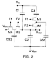
- FIG. 2 Shown in Figure 2 is a circuit diagram for an AC coupler according to the invention which can be implemented in the switched-capacitor form.
- Both these terminals may, however, be connected to the same reference potential, e.g. to ground.
- the scheme comprises two capacitors, C1 and C2, which are respectively connected between an input terminal Vin and an output terminal Vout, and between said output terminal and the first terminal, Vref1, of connection to a reference potential.
- capacitor C1 Connected serially together and in parallel with the capacitor C1 are a capacitor C3 and two field-effect transistors M1 and M2.
- Two more field-effect transistors, M3 and M4, are connected between the output terminal Vout and the second terminal, Vref2, of connection to a reference potential.
- connection nodes between the transistors M1 and M2, and between the transistors M3 and M4, are coupled through capacitors Cs1 and Cs2, respectively, to the first terminal, Vref1, of connection to a reference potential.
- control signals F1 and F2 generated by a control signal generator at two non-overlapping time phases, which signals may be also referred to as clock signals, usually at a frequency of 64 kHz in telephone applications.
- Optimum matching of the frequencies involved can be achieved using switched-capacitor techniques.
- a practical problem encountered with the solution shown in Figure 2 is that the transistors M1 and M2 are connected to the voltage Vin through the capacitor C3 which represents a short circuit in the band of interest.
- the signal applied to the terminal Vin is transferred to the connection node between the capacitor C3 and the transistor M1.
- said node has a wide dynamic range and requires that high clock voltages be used for it to operate properly.
- a further problem is that upon turning on, the node value may become equal to Vin (12 Vmax), and this voltage cannot be accepted by MOS devices having a maximum operating voltage of 5 Volts.
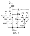
- FIG. 3 Shown in Figure 3 is the circuit diagram of an AC coupler according to the invention, which can also obviate these drawbacks, but at the expense of a slight increase in integration area.
- a unitary gain AC interface circuit means B replaces the capacitor C3 and, unlike the latter, is connected between the output terminal Vout and the transistor pair M1, M2.
- the scheme of Figure 3 further comprises a capacitor C4, connected in series with the capacitor C3 between the output terminal and the terminal Vref1 of connection to a reference potential.
- the transistor pair M1, M2 are connected here to a connection node between the capacitor C3 and C4.
- the signal on the node is approximately one fourth the signal Vin.
- the transistors at Vin (line) appear to be reduced by a factor of four on account of the capacitive divider.
- the dynamic range on the node can be set at 4 Volts.
Landscapes
- Engineering & Computer Science (AREA)
- Signal Processing (AREA)
- Networks Using Active Elements (AREA)
- Filters And Equalizers (AREA)
Claims (7)
- Wechselstrom-Koppel- und Gleichstrom-Entkoppel-Schaltung, dadurch gekennzeichnet, daß sie eine Übertragungsfunktion mit einem Pol und einer Nullstelle bei ähnlichen Frequenzen zwischen einem ersten Pol und dem interessierenden Frequenzband für die Kompensation des durch den ersten Pol erzeugten Phasenfehlers aufweist.
- Schaltung nach Anspruch 1, mit mindestens einem Eingangsanschluß (Vin) und einem Ausgangsanschluß (Vout) und mindestens einem ersten (Vref1) und einem zweiten (Vref2) Anschluß für die Verbindung mit einem Referenzpotential, dadurch gekennzeichnet, daß sie aufweist: ein erstes (C1) und ein zweites (C2) kapazitives Element, die in Reihe zusammengeschaltet sind zwischen dem Eingangsanschluß (Vin) und dem Ausgangsanschluß (Vout) bzw. zwischen dem Ausgangsanschluß und dem ersten Anschluß (Vref1) für die Verbindung mit einem Referenzpotential, daß sie ein drittes kapazitives Element (C3) und einen ersten und einen zweiten Feldeffekttransistor (M1, M2), die über ihre Source- und Drain-Anschlüsse geschaltet sind, aufweist, wobei das dritte kapazitive Element (C3) zwischen den Eingangsanschluß und den Ausgangsanschluß (Vout) geschaltet ist, und daß sie einen dritten und einen vierten Feldeffekttransistor (M3, M4) aufweist, die in Reihe über ihre Source- und Drainanschlüsse zusammengeschaltet sind zwischen dem Ausgangsanschluß (Vout) und dem zweiten Anschluß (Vref2) für den Anschluß an ein Referenzpotential, wobei die Verbindungsknoten zwischen dem ersten und dem zweiten Transistor (M1, M2) und zwischen dem dritten und dem vierten Transistor (M3, M4) über kapazitive Elemente (CS1, CS2) an den ersten Anschluß (Vref1) für den Anschluß an ein Referenzpotential angeschlossen sind, und die Gate-Anschlüsse der Transistoren für den Anschluß an einen Steuersignalgenerator mit zwei nicht einander überlappenden Phasen ausgebildet sind.
- Schaltung nach Anspruch 2, dadurch gekennzeichnet, daß die kapazitiven Elemente selbst monolithisch in der Schaltung integriert sind.
- Schaltung nach Anspruch 3, dadurch gekennzeichnet, daß der erste und der vierte Transistor (M1, M4) von Steuersignalen angesteuert werden, deren Phase sich nicht mit derjenigen der den zweiten und den dritten Transistor (M2, M3) ansteuernden Steuersignale überlappt.
- Schaltung nach Anspruch 1 mit mindestens einem Eingangsanschluß (Vin) und einem Ausgangsanschluß (Vout), und mindestens einem ersten (Vref1) und einem zweiten (Vref2) Anschluß für die Verbindung mit einem Referenzpotential, dadurch gekennzeichnet, daß sie ein erstes (C1) und ein zweites (C2) kapazitives Element enthält, die in Reihe zusammengeschaltet sind zwischen dem Eingangsanschluß (Vin) und dem Ausgangsanschluß (Vout) bzw. zwischen dem Ausgangsanschluß (Vout) und dem ersten Anschluß (Vref1) für die Verbindung mit einem Referenzpotential, und mindestens eine Wechselstrom-Schnittstellenschaltung (B) mit der Verstärkung von eins aufweist, sowie ein drittes (C3) und ein viertes (C4) kapazitives Element, die in Reihe zusammengeschaltet sind und parallel zu dem zweiten kapazitiven Element (C2) geschaltet sind, daß sie mindestens einen ersten und einen zweiten Feldeffekttransistor (M1, M2) enthält, die in Reihe über ihre Source- und Drainanschlüsse zusammengeschaltet sind zwischen einem Verbindungsschaltungsknoten des dritten (C3) und des vierten (C4) kapazitiven Elements und einem Ausgangsanschluß der Schnittstellenschaltung (B), die mit einem Eingangsanschluß an den Ausgangsanschluß der Schaltung angeschlossen ist, und mindestens einen dritten und einen vierten Feldeffekttransistor (M3, M4), die über ihre Source- und Drainanschlüsse in Reihe geschaltet sind zwischen den Ausgangsanschluß (Vout) und dem zweiten Anschluß (Vref2) für die Verbindung mit einem Referenzpotential, wobei ein Verbindungsschaltungsknoten des ersten und des zweiten Transistors (M1, M2) und ein Verbindungsschaltungsknoten des dritten und des vierten Transistors (M3, M4) über kapazitive Elemente (CS1, CS2) an den ersten Anschluß für die Verbindung mit einem Referenzpotential (Vref) gekoppelt sind, und die Gateanschlüsse der Transistoren (M1, M2, M3, M4) ausgebildet sind für den Anschluß an einen Steuersignalgenerator, der zwei nicht-überlappende Phasen aufweist.
- Schaltung nach Anspruch 5, dadurch gekennzeichnet, daß die kapazitiven Elemente in der Schaltung selbst monolithisch integriert sind.
- Schaltung nach Anspruch 6, dadurch gekennzeichnet, daß der erste und der vierte Transistor (M1, M4) von Steuersignalen angesteuert werden, deren Phase sich nicht überlappt mit derjenigen der Steuersignale, die den zweiten und den dritten Transistor (M2, M3) ansteuert.
Priority Applications (4)
| Application Number | Priority Date | Filing Date | Title |
|---|---|---|---|
| DE69229734T DE69229734T2 (de) | 1992-10-30 | 1992-10-30 | Integrierte Kopplungsschaltung für Wechselstrom mit Phasenausgleich |
| EP92830603A EP0594922B1 (de) | 1992-10-30 | 1992-10-30 | Integrierte Kopplungsschaltung für Wechselstrom mit Phasenausgleich |
| US08/140,233 US5610564A (en) | 1992-10-30 | 1993-10-20 | AC integrated coupler with phase equalizer |
| JP5273559A JPH06276044A (ja) | 1992-10-30 | 1993-11-01 | 交流結合回路 |
Applications Claiming Priority (1)
| Application Number | Priority Date | Filing Date | Title |
|---|---|---|---|
| EP92830603A EP0594922B1 (de) | 1992-10-30 | 1992-10-30 | Integrierte Kopplungsschaltung für Wechselstrom mit Phasenausgleich |
Publications (2)
| Publication Number | Publication Date |
|---|---|
| EP0594922A1 EP0594922A1 (de) | 1994-05-04 |
| EP0594922B1 true EP0594922B1 (de) | 1999-08-04 |
Family
ID=8212196
Family Applications (1)
| Application Number | Title | Priority Date | Filing Date |
|---|---|---|---|
| EP92830603A Expired - Lifetime EP0594922B1 (de) | 1992-10-30 | 1992-10-30 | Integrierte Kopplungsschaltung für Wechselstrom mit Phasenausgleich |
Country Status (4)
| Country | Link |
|---|---|
| US (1) | US5610564A (de) |
| EP (1) | EP0594922B1 (de) |
| JP (1) | JPH06276044A (de) |
| DE (1) | DE69229734T2 (de) |
Families Citing this family (1)
| Publication number | Priority date | Publication date | Assignee | Title |
|---|---|---|---|---|
| EP3914917A1 (de) | 2019-01-22 | 2021-12-01 | Stmicroelectronics Sa | Verfahren und vorrichtung zur phasendetektion eines signals über einen hybridkoppler unter verwendung einer referenzphase |
Family Cites Families (3)
| Publication number | Priority date | Publication date | Assignee | Title |
|---|---|---|---|---|
| US3114117A (en) * | 1960-05-20 | 1963-12-10 | Bell Telephone Labor Inc | Tunable rc oscillator |
| DE2064517A1 (de) * | 1970-12-30 | 1972-07-13 | Siemens Ag | Tiefpaßschaltung für elektrische Schwingungen |
| US4801888A (en) * | 1988-02-29 | 1989-01-31 | Maxim Integrated Products | Programmable, universal filter with self biasing |
-
1992
- 1992-10-30 DE DE69229734T patent/DE69229734T2/de not_active Expired - Fee Related
- 1992-10-30 EP EP92830603A patent/EP0594922B1/de not_active Expired - Lifetime
-
1993
- 1993-10-20 US US08/140,233 patent/US5610564A/en not_active Expired - Lifetime
- 1993-11-01 JP JP5273559A patent/JPH06276044A/ja active Pending
Also Published As
| Publication number | Publication date |
|---|---|
| US5610564A (en) | 1997-03-11 |
| DE69229734T2 (de) | 2000-03-02 |
| EP0594922A1 (de) | 1994-05-04 |
| DE69229734D1 (de) | 1999-09-09 |
| JPH06276044A (ja) | 1994-09-30 |
Similar Documents
| Publication | Publication Date | Title |
|---|---|---|
| US4803382A (en) | Voltage comparator circuit | |
| JPS63157515A (ja) | フィルター回路 | |
| EP0415080B1 (de) | Vorrichtung zur Umwandlung von elektrischen analogen unsymmetrischen Signalen in vollständig differentielle Signale | |
| US4728811A (en) | Sample-and-hold circuit | |
| US4647865A (en) | Parasitic insensitive switched capacitor input structure for a fully differential operational amplifier | |
| JPH0119653B2 (de) | ||
| CN110048710A (zh) | 一种电压信号隔离转换系统 | |
| US5477186A (en) | Chopper type differential amplifier using MOS gate capacitors | |
| EP0594922A1 (de) | Integrierte Kopplungsschaltung für Wechselstrom mit Phasenausgleich | |
| KR19980018571A (ko) | 전자 회로 및 저항기 네트워크 | |
| CN100454761C (zh) | 开关电容器电路结构 | |
| JPH037910B2 (de) | ||
| EP0769848B1 (de) | Verstärkerstufe und Verfahren für Nullpunktsspannungsunterdrückung | |
| US5717364A (en) | Mixer | |
| US5204982A (en) | Method and apparatus for digital switching of fm signals with reduced crosstalk | |
| GB2157108A (en) | Eliminating input offset | |
| EP0105369B1 (de) | Kombinierter phasendetektor und tiefpassfilter | |
| US4338656A (en) | Voltage polarity switching circuit | |
| US6392454B1 (en) | Shunt regulated push-pull circuit having wide frequency range | |
| US7382197B2 (en) | Adaptive tuning circuit to maximize output signal amplitude for an amplifier | |
| CN119420382B (zh) | 一种用于直流电源载波通讯的有源电感 | |
| JPH0660688A (ja) | サンプル・ホールド回路 | |
| CN1019708B (zh) | 取样保持电路 | |
| JPH0363848B2 (de) | ||
| CN209748523U (zh) | 一种电压信号隔离转换系统 |
Legal Events
| Date | Code | Title | Description |
|---|---|---|---|
| PUAI | Public reference made under article 153(3) epc to a published international application that has entered the european phase |
Free format text: ORIGINAL CODE: 0009012 |
|
| AK | Designated contracting states |
Kind code of ref document: A1 Designated state(s): DE FR GB IT |
|
| 17P | Request for examination filed |
Effective date: 19940722 |
|
| 17Q | First examination report despatched |
Effective date: 19970520 |
|
| RAP3 | Party data changed (applicant data changed or rights of an application transferred) |
Owner name: STMICROELECTRONICS S.R.L. |
|
| GRAG | Despatch of communication of intention to grant |
Free format text: ORIGINAL CODE: EPIDOS AGRA |
|
| GRAG | Despatch of communication of intention to grant |
Free format text: ORIGINAL CODE: EPIDOS AGRA |
|
| GRAH | Despatch of communication of intention to grant a patent |
Free format text: ORIGINAL CODE: EPIDOS IGRA |
|
| GRAH | Despatch of communication of intention to grant a patent |
Free format text: ORIGINAL CODE: EPIDOS IGRA |
|
| GRAA | (expected) grant |
Free format text: ORIGINAL CODE: 0009210 |
|
| AK | Designated contracting states |
Kind code of ref document: B1 Designated state(s): DE FR GB IT |
|
| REF | Corresponds to: |
Ref document number: 69229734 Country of ref document: DE Date of ref document: 19990909 |
|
| ITF | It: translation for a ep patent filed | ||
| ET | Fr: translation filed | ||
| PLBE | No opposition filed within time limit |
Free format text: ORIGINAL CODE: 0009261 |
|
| 26N | No opposition filed | ||
| REG | Reference to a national code |
Ref country code: GB Ref legal event code: IF02 |
|
| PGFP | Annual fee paid to national office [announced via postgrant information from national office to epo] |
Ref country code: DE Payment date: 20030930 Year of fee payment: 12 |
|
| PGFP | Annual fee paid to national office [announced via postgrant information from national office to epo] |
Ref country code: GB Payment date: 20040929 Year of fee payment: 13 |
|
| PGFP | Annual fee paid to national office [announced via postgrant information from national office to epo] |
Ref country code: FR Payment date: 20041025 Year of fee payment: 13 |
|
| PG25 | Lapsed in a contracting state [announced via postgrant information from national office to epo] |
Ref country code: DE Free format text: LAPSE BECAUSE OF NON-PAYMENT OF DUE FEES Effective date: 20050503 |
|
| PG25 | Lapsed in a contracting state [announced via postgrant information from national office to epo] |
Ref country code: IT Free format text: LAPSE BECAUSE OF NON-PAYMENT OF DUE FEES;WARNING: LAPSES OF ITALIAN PATENTS WITH EFFECTIVE DATE BEFORE 2007 MAY HAVE OCCURRED AT ANY TIME BEFORE 2007. THE CORRECT EFFECTIVE DATE MAY BE DIFFERENT FROM THE ONE RECORDED. Effective date: 20051030 Ref country code: GB Free format text: LAPSE BECAUSE OF NON-PAYMENT OF DUE FEES Effective date: 20051030 |
|
| GBPC | Gb: european patent ceased through non-payment of renewal fee |
Effective date: 20051030 |
|
| PG25 | Lapsed in a contracting state [announced via postgrant information from national office to epo] |
Ref country code: FR Free format text: LAPSE BECAUSE OF NON-PAYMENT OF DUE FEES Effective date: 20060630 |
|
| REG | Reference to a national code |
Ref country code: FR Ref legal event code: ST Effective date: 20060630 |