EP0595069A1 - Etage commutateur de courant - Google Patents
Etage commutateur de courant Download PDFInfo
- Publication number
- EP0595069A1 EP0595069A1 EP93116009A EP93116009A EP0595069A1 EP 0595069 A1 EP0595069 A1 EP 0595069A1 EP 93116009 A EP93116009 A EP 93116009A EP 93116009 A EP93116009 A EP 93116009A EP 0595069 A1 EP0595069 A1 EP 0595069A1
- Authority
- EP
- European Patent Office
- Prior art keywords
- emitter
- comparison device
- output
- bipolar transistor
- input
- Prior art date
- Legal status (The legal status is an assumption and is not a legal conclusion. Google has not performed a legal analysis and makes no representation as to the accuracy of the status listed.)
- Granted
Links
- 238000000034 method Methods 0.000 description 3
- 230000007423 decrease Effects 0.000 description 2
- 238000010586 diagram Methods 0.000 description 2
- 238000007599 discharging Methods 0.000 description 1
- 230000000694 effects Effects 0.000 description 1
- 230000007704 transition Effects 0.000 description 1
Images
Classifications
-
- H—ELECTRICITY
- H03—ELECTRONIC CIRCUITRY
- H03K—PULSE TECHNIQUE
- H03K19/00—Logic circuits, i.e. having at least two inputs acting on one output; Inverting circuits
- H03K19/02—Logic circuits, i.e. having at least two inputs acting on one output; Inverting circuits using specified components
- H03K19/08—Logic circuits, i.e. having at least two inputs acting on one output; Inverting circuits using specified components using semiconductor devices
- H03K19/082—Logic circuits, i.e. having at least two inputs acting on one output; Inverting circuits using specified components using semiconductor devices using bipolar transistors
- H03K19/086—Emitter coupled logic
-
- H—ELECTRICITY
- H03—ELECTRONIC CIRCUITRY
- H03K—PULSE TECHNIQUE
- H03K19/00—Logic circuits, i.e. having at least two inputs acting on one output; Inverting circuits
- H03K19/01—Modifications for accelerating switching
- H03K19/013—Modifications for accelerating switching in bipolar transistor circuits
- H03K19/0136—Modifications for accelerating switching in bipolar transistor circuits by means of a pull-up or down element
Definitions
- the invention relates to a switching stage with a differential amplifier arrangement, with a first bipolar transistor which is connected in an emitter follower circuit to an output of the differential amplifier arrangement and whose emitter is connected to an output of the switching stage, with a current source which is between the output of the switching stage and a connection for a Supply potential is connected to a further bipolar transistor in an emitter follower circuit, which is connected to the output of the differential amplifier arrangement, the emitter of the first bipolar transistor being connected to a first input of a comparison device and the emitter of the further bipolar transistor being connected to a second input of the comparison device, the current source is a controllable current source with a control input which is connected to an output of the comparison device, and wherein the controllable current source is controlled by the comparison device such that e is impressed in high current from the current source if the potential of the emitter of the first bipolar transistor is higher than the potential of the emitter of the further bipolar transistor and that otherwise a low current is impressed.
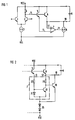
- Such a switching stage is known from EP 0 367 612 A2 and is shown in FIG. 1 by a basic circuit diagram.
- the comparison device is provided by a differential amplifier, which has two transistors is formed, the emitters of which are connected to a reference potential via a current source.
- the controllable power source is constructed in two stages.
- EP 0 438 953 A1 also discloses a switching stage with a differential amplifier, two bipolar transistors and a comparison circuit which controls a current source and is provided by a current mirror circuit. In this switching stage, however, the two bipolar transistors are driven by differential amplifier outputs of different polarities.
- JP 2-231 814 (A) from Patent Abstracts of Japan, 1990, Vol. 14, No. 541, E-1007 also discloses a switching stage with a differential amplifier, two bipolar transistors and a comparison circuit which drives a current source.
- the comparison circuit there is formed with a two-stage current switch.
- the bipolar transistors are each controlled by a different output of the differential amplifier.
- the comparison device contains a current mirror circuit with an input branch and an output branch, that the input branch and the output branch each have a first and a second connection, that the first connection of the input branch, the second input of the comparison device and the first connection of the Output branch of the first input of the comparison device is that the input branch with the series connection is formed from a first resistor and a forward polarized diode that the output branch is formed with the series circuit of a second resistor and a transistor, the base of which is connected to the anode of the diode and the collector of which is connected to the output of the comparator, and that The cathode of the diode and the emitter of the transistor form the second connections of the comparison device and are connected to the connection for the supply potential or that the comparison device contains a bipolar transistor, the base and the emitter of which are each connected via a resistor to the connection for the supply potential that the base of the bipolar transistor is connected to the second input of the comparison device and that the collector of the bipolar transistor is
- a switching stage according to the invention has the advantage that the current impressed by the controllable current source is only high when it is required for reloading the load capacity. Otherwise the current is low.
- the current source can be dimensioned such that the negative switching edge is sufficiently steep according to the speed requirements, while the power loss remains low.
- the design of the comparison device as a current mirror circuit has the advantage that the output level is largely unaffected by fluctuations in the supply voltage.
- the controllable current source can be designed as a bipolar transistor. By means of at least one diode, which is between the emitter and the connection for the supply potential is switched, the base-emitter voltage of the bipolar transistor is reduced. This has the advantage that the bipolar transistor can be dimensioned for a lower voltage load.
- the switching stage of FIG. 1 contains a differential amplifier arrangement which carries out a logic function and which is followed by an output stage for driving the load capacitances.
- the differential amplifier arrangement contains two emitter-coupled bipolar transistors 1, 2, the emitters of which are connected via a current source 3 to a connection for a negative supply potential VEE.
- the collectors of transistors 1, 2 are connected to a connection for a positive supply potential VCC.
- a load resistor 4 is connected in the collector circuit of transistor 2.
- the base of transistor 1 is controlled by an input signal the base of transistor 2 from a reference signal.
- the output 14 of the differential amplifier arrangement is the collector-side connection of the resistor 4. This is connected to the base connections of two bipolar transistors 5, 6.
- the transistors 5, 6 are connected in the emitter follower circuit with respect to the output of the differential amplifier arrangement.
- the emitter of the bipolar transistor 6 is connected to an output 10 of the switching stage. Further circuits and connecting lines connected to the output 10 essentially act as a capacitive load 9.
- the output 10 is connected to the potential VEE via a controllable current source 8.
- the controllable current source 8 has a control input 11 which is connected to the output of a comparison device 7.
- the inputs 12, 13 of the comparison device 7 are connected to the loaded emitter of the transistor 6 and the unloaded emitter of the transistor 5, respectively.
- the comparison device 7 is constructed in such a way that it only generates a signal at its output, by means of which a high current can be set in the current source 8 when the emitter of the transistor 5 is at a lower potential than the emitter of the transistor 6. In the others Operating states, that is, when the emitter potentials of the transistors 5, 6 are approximately the same or the emitter of the transistor 5 has a higher potential than the emitter of the transistor 6, the comparison device 7 generates a signal by means of which a low current can be set in the current source 8.
- the emitter potential of the transistor 5 largely follows the collector potential of the transistor 2 without delay, since the emitter of the transistor 5 is not capacitively loaded by the output load is.
- the emitter potential of the transistor 6 initially follows the collector potential of the transistor 2 with a time delay.
- This potential difference at the inputs of the comparison device 7 generates a signal at its output, by means of which the current source 8 is controlled in such a way that a high current flows.
- the capacitance 9 is charged, as a result of which the emitter potential of the transistor 6 drops and the potential difference at the inputs of the comparison device 7 decreases.
- the current of the current source 8 is then controlled low again.
- the reverse switching process that is, in the case of a transition from an L to an H level, the potential difference at the inputs of the comparison device 7 is such that the current of the current source 8 is set low.
- the current for discharging the load capacitance 9 flows here via the collector-emitter path of the transistor 6.
- This switching stage has the advantage that the current of the current source 8 is only high when the current required to charge the capacitance 9 flows via the current source 8 to the connection for the supply potential VEE, that is when switching from H to L. Power loss the negative edge can be set relatively steep. With such a circuit stage, a high operating speed with low power loss is made possible.
- the comparison device 7 contains a current mirror circuit with an input branch and an output branch: These are each connected at a first connection to the emitter of the transistor 5 or the emitter of the transistor 6.
- Both branches are coupled to a second connection and connected to the supply potential VEE.
- the input branch contains a diode 21 which is connected in parallel to the base-emitter path of a bipolar transistor 22.
- a resistor 23 is arranged between the diode 21 and the emitter of the transistor 5.
- Another resistor 24 is connected between the collector of transistor 22 and the emitter of transistor 6.
- the collector of the transistor serves as the output of the comparison device 7. It is connected to the control input of the current source 8, which is designed as a bipolar transistor 20.
- the collector of the bipolar transistor 20 is connected to the output 10 of the switching stage, the emitter to the supply potential VEE.
- the coupled second connections of the input and output branches of the current mirror circuit are coupled to the emitter of the current source transistor 20, wherein they are connected to the connection for the supply potential VEE via two diodes 25.
- the diodes 25 have the effect that the transistor 20 and the elements of the comparison device 7 can be designed for a lower working voltage.
- the emitter potential of the unloaded transistor 5 drops relatively quickly.
- the voltage drop across the resistor 23 is reduced, so that the current in the input branch 21, 23 of the current mirror circuit decreases.
- the lower current - mirrored in the output branch 22, 24 - produces a lower current drop across the resistor 24.
- the emitter potential of the loaded emitter of the transistor 6 is still largely at H. This has the consequence that the base potential of the transistor 20 is high and the transistor 20 conducts.
- the capacitance 90 is now charged via the transistor 20.
- the emitter potential of the transistor 6 drops to L, as a result of which the transistor 20 becomes high-resistance if the components are dimensioned accordingly.
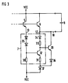
- FIG. 3 contains a further embodiment according to the invention for the comparison device 7.
- the controlled current source is implemented as a bipolar transistor 20, the emitter of which is connected to the connection for the supply potential VEE via two diodes 36, 37.
- the comparison device 7 has a first current path which contains a resistor 30 which is connected to the supply potential VEE with one connection and to the emitter of the transistor 5 with another connection via two diodes 35.
- a second current path contains the collector-emitter path of a bipolar transistor 32, the base of which is connected to the other connection of the resistor 30.
- the emitter of the bipolar transistor 32 is connected to the supply potential VEE via a resistor 31.
- the resistor 31 can - as shown in FIG. 3 - be connected via the diode 37 to the connection for the supply potential VEE.
- the collector of the bipolar transistor 30 serves as the output of the comparison device 7. It is connected to the emitter of the transistor 6 via a resistor 33 and a diode 34.
- the voltage across the resistor 30 is reduced, as a result of which the resistance of the collector-emitter path of the transistor 32 increases and the current is reduced. This has the consequence that the voltage drop across the resistor 33 becomes smaller and thus the collector potential of the transistor 32 increases.
- the current source transistor 20 then conducts strongly. As a result, the capacity 9 is charged. When the potential at the output 10 drops, the current source transistor 20 becomes high-resistance.
- the diodes 34, ..., 37 are used for the potential shift, so that the components can be dimensioned for lower working voltages. In principle, it is possible to remove the diode 34 and one of the diodes 35. On the other hand, further diodes can be inserted between the resistors 30, 31 and the connection for the supply potential VEE.
Landscapes
- Engineering & Computer Science (AREA)
- Physics & Mathematics (AREA)
- Computer Hardware Design (AREA)
- Computing Systems (AREA)
- General Engineering & Computer Science (AREA)
- Mathematical Physics (AREA)
- Power Engineering (AREA)
- Electronic Switches (AREA)
- Logic Circuits (AREA)
Applications Claiming Priority (2)
| Application Number | Priority Date | Filing Date | Title |
|---|---|---|---|
| DE4236430 | 1992-10-28 | ||
| DE4236430A DE4236430C1 (de) | 1992-10-28 | 1992-10-28 | Schaltstufe in Stromschaltertechnik |
Publications (2)
| Publication Number | Publication Date |
|---|---|
| EP0595069A1 true EP0595069A1 (fr) | 1994-05-04 |
| EP0595069B1 EP0595069B1 (fr) | 1997-08-06 |
Family
ID=6471581
Family Applications (1)
| Application Number | Title | Priority Date | Filing Date |
|---|---|---|---|
| EP93116009A Expired - Lifetime EP0595069B1 (fr) | 1992-10-28 | 1993-10-04 | Etage commutateur de courant |
Country Status (4)
| Country | Link |
|---|---|
| US (1) | US5397938A (fr) |
| EP (1) | EP0595069B1 (fr) |
| JP (1) | JP3412702B2 (fr) |
| DE (2) | DE4236430C1 (fr) |
Families Citing this family (23)
| Publication number | Priority date | Publication date | Assignee | Title |
|---|---|---|---|---|
| US5781046A (en) * | 1995-03-22 | 1998-07-14 | Vtc, Inc. | Push-and-pull driver circuit for driving an H-bridge coupled to a two-terminal inductive load |
| US5751171A (en) * | 1995-03-22 | 1998-05-12 | Vtc Inc. | Predriver for fast current switching through a two-terminal inductive load |
| US5909127A (en) * | 1995-12-22 | 1999-06-01 | International Business Machines Corporation | Circuits with dynamically biased active loads |
| DE19635024C1 (de) * | 1996-08-29 | 1997-10-16 | Siemens Ag | Schaltungsanordnung zum Treiben einer kapazitiven Last |
| US7002401B2 (en) * | 2003-01-30 | 2006-02-21 | Sandisk Corporation | Voltage buffer for capacitive loads |
| JP2006311419A (ja) * | 2005-05-02 | 2006-11-09 | Nec Electronics Corp | 信号出力回路 |
| US8901845B2 (en) | 2009-09-24 | 2014-12-02 | Cree, Inc. | Temperature responsive control for lighting apparatus including light emitting devices providing different chromaticities and related methods |
| US9713211B2 (en) | 2009-09-24 | 2017-07-18 | Cree, Inc. | Solid state lighting apparatus with controllable bypass circuits and methods of operation thereof |
| US10264637B2 (en) | 2009-09-24 | 2019-04-16 | Cree, Inc. | Solid state lighting apparatus with compensation bypass circuits and methods of operation thereof |
| US8901829B2 (en) * | 2009-09-24 | 2014-12-02 | Cree Led Lighting Solutions, Inc. | Solid state lighting apparatus with configurable shunts |
| US8777449B2 (en) * | 2009-09-25 | 2014-07-15 | Cree, Inc. | Lighting devices comprising solid state light emitters |
| US9068719B2 (en) * | 2009-09-25 | 2015-06-30 | Cree, Inc. | Light engines for lighting devices |
| US8602579B2 (en) * | 2009-09-25 | 2013-12-10 | Cree, Inc. | Lighting devices including thermally conductive housings and related structures |
| US9285103B2 (en) * | 2009-09-25 | 2016-03-15 | Cree, Inc. | Light engines for lighting devices |
| US8476836B2 (en) * | 2010-05-07 | 2013-07-02 | Cree, Inc. | AC driven solid state lighting apparatus with LED string including switched segments |
| US9839083B2 (en) | 2011-06-03 | 2017-12-05 | Cree, Inc. | Solid state lighting apparatus and circuits including LED segments configured for targeted spectral power distribution and methods of operating the same |
| US9131561B2 (en) | 2011-09-16 | 2015-09-08 | Cree, Inc. | Solid-state lighting apparatus and methods using energy storage |
| US8742671B2 (en) | 2011-07-28 | 2014-06-03 | Cree, Inc. | Solid state lighting apparatus and methods using integrated driver circuitry |
| US8791641B2 (en) | 2011-09-16 | 2014-07-29 | Cree, Inc. | Solid-state lighting apparatus and methods using energy storage |
| US11178740B2 (en) * | 2011-12-27 | 2021-11-16 | Ideal Industries Lighting Llc | Solid-state lighting apparatus including current diversion controlled by lighting device bias states and current limiting using a passive electrical component |
| US9131571B2 (en) | 2012-09-14 | 2015-09-08 | Cree, Inc. | Solid-state lighting apparatus and methods using energy storage with segment control |
| US10264638B2 (en) | 2013-01-15 | 2019-04-16 | Cree, Inc. | Circuits and methods for controlling solid state lighting |
| US10231300B2 (en) | 2013-01-15 | 2019-03-12 | Cree, Inc. | Systems and methods for controlling solid state lighting during dimming and lighting apparatus incorporating such systems and/or methods |
Citations (3)
| Publication number | Priority date | Publication date | Assignee | Title |
|---|---|---|---|---|
| WO1985004774A1 (fr) * | 1984-04-06 | 1985-10-24 | Advanced Micro Devices, Inc. | Circuit d'attaque de ligne independant des variations de la tension d'alimentation et de la recherche de temperature pour des circuits de logique a couplage par l'emetteur |
| EP0294163A2 (fr) * | 1987-06-02 | 1988-12-07 | Fujitsu Limited | Circuit intégré à semi-conducteurs comportant un circuit émetteur-suiveur |
| US5079448A (en) * | 1989-10-13 | 1992-01-07 | Nec Corporation | Emitter-follower circuit in which load capacitance is quickly discharged |
Family Cites Families (9)
| Publication number | Priority date | Publication date | Assignee | Title |
|---|---|---|---|---|
| EP0036712A3 (en) * | 1980-03-01 | 1981-11-25 | Bp Chemicals Limited | Heterogeneous esterification catalyst, process for its production and its use in the production of residue esters |
| JPS6177424A (ja) * | 1984-09-25 | 1986-04-21 | Fujitsu Ltd | Ecl回路 |
| DE3714936A1 (de) * | 1987-05-05 | 1988-12-08 | Wifag Maschf | Farbwerk fuer eine druckmaschine |
| JPS63302620A (ja) * | 1987-06-03 | 1988-12-09 | Toshiba Corp | 出力回路 |
| US4948991A (en) * | 1988-11-03 | 1990-08-14 | Motorola Inc. | Load controlled ECL transient driver |
| US4980582A (en) * | 1989-02-03 | 1990-12-25 | National Semiconductor Corporation | High speed ECL input buffer for vertical fuse arrays |
| US5013941A (en) * | 1989-08-17 | 1991-05-07 | National Semiconductor Corporation | TTL to ECL/CML translator circuit |
| US5012128A (en) * | 1990-01-24 | 1991-04-30 | International Business Machines Corporation | High speed push-pull driver having current mirror pull-down |
| JPH0461419A (ja) * | 1990-06-29 | 1992-02-27 | Nec Corp | Ecl回路 |
-
1992
- 1992-10-28 DE DE4236430A patent/DE4236430C1/de not_active Expired - Lifetime
-
1993
- 1993-10-04 EP EP93116009A patent/EP0595069B1/fr not_active Expired - Lifetime
- 1993-10-04 DE DE59307065T patent/DE59307065D1/de not_active Expired - Fee Related
- 1993-10-25 JP JP28724893A patent/JP3412702B2/ja not_active Expired - Fee Related
- 1993-10-28 US US08/144,574 patent/US5397938A/en not_active Expired - Lifetime
Patent Citations (3)
| Publication number | Priority date | Publication date | Assignee | Title |
|---|---|---|---|---|
| WO1985004774A1 (fr) * | 1984-04-06 | 1985-10-24 | Advanced Micro Devices, Inc. | Circuit d'attaque de ligne independant des variations de la tension d'alimentation et de la recherche de temperature pour des circuits de logique a couplage par l'emetteur |
| EP0294163A2 (fr) * | 1987-06-02 | 1988-12-07 | Fujitsu Limited | Circuit intégré à semi-conducteurs comportant un circuit émetteur-suiveur |
| US5079448A (en) * | 1989-10-13 | 1992-01-07 | Nec Corporation | Emitter-follower circuit in which load capacitance is quickly discharged |
Also Published As
| Publication number | Publication date |
|---|---|
| EP0595069B1 (fr) | 1997-08-06 |
| US5397938A (en) | 1995-03-14 |
| JPH06224720A (ja) | 1994-08-12 |
| DE59307065D1 (de) | 1997-09-11 |
| JP3412702B2 (ja) | 2003-06-03 |
| DE4236430C1 (de) | 1994-02-17 |
Similar Documents
| Publication | Publication Date | Title |
|---|---|---|
| EP0595069B1 (fr) | Etage commutateur de courant | |
| EP0096944B1 (fr) | Circuit avec plusieurs chemins de signaux formés par des composants actifs | |
| EP0762651B1 (fr) | Circuit d'attaque pour une diode photoémettrice | |
| DE1762172C3 (de) | Verknüpfungsschaltung mit Stromübernahmeschaltern | |
| DE69320326T2 (de) | Mit niedriger Versorgungsspannung arbeitender, eine Hysteresis aufweisender Komparator | |
| DE3587924T2 (de) | Schaltung zur Beschleunigung des Hoch-Tief-Überganges für TTL-Gatter. | |
| DE2306994C3 (de) | Gegentakt-Treiberschaltung | |
| EP0583688B1 (fr) | Commutateur numérique de courant | |
| DE3486360T2 (de) | Differentialschalter. | |
| EP0078335B1 (fr) | Procédé de lecture d'une mémoire à semi-conducteurs | |
| EP0334447A2 (fr) | Circuit déclencheur de Schmitt | |
| DE4409453A1 (de) | BiCMOS-Pegelwandler ECL-CMOS | |
| DE69630018T2 (de) | Logische schaltung für niedrige spannungen | |
| DE69118219T2 (de) | ECL-Schaltung in einem integrierten Halbleiterschaltkreis | |
| DE3518413C2 (de) | Eingangspufferschaltung und diese verwendende Logikschaltung | |
| DE69119283T2 (de) | ECL/TTL-Pegelumsetzer | |
| DE3318957A1 (de) | Monolithisch integrierbare, bistabile multivibratorschaltung mit einem in einen vorzugszustand einstellbaren ausgang | |
| EP0588111B1 (fr) | Elément de mémoire | |
| DE69223987T2 (de) | Symmetrische schaltung zur schnellen spannungsschaltung | |
| DE3311258C1 (de) | Schaltungsanordnung zur UEberwachung einer Betriebsspannung | |
| DE19605248C1 (de) | Treiberschaltung | |
| EP0635942A2 (fr) | Etage de commutation numérique avec commutateur de courant | |
| DE69223658T2 (de) | Ausgangstufe für eine digitale Schaltung | |
| DE4222170C1 (fr) | ||
| DE68910964T2 (de) | Stromquelletechnologie. |
Legal Events
| Date | Code | Title | Description |
|---|---|---|---|
| PUAI | Public reference made under article 153(3) epc to a published international application that has entered the european phase |
Free format text: ORIGINAL CODE: 0009012 |
|
| AK | Designated contracting states |
Kind code of ref document: A1 Designated state(s): DE FR GB IT |
|
| 17P | Request for examination filed |
Effective date: 19940608 |
|
| 17Q | First examination report despatched |
Effective date: 19960424 |
|
| GRAG | Despatch of communication of intention to grant |
Free format text: ORIGINAL CODE: EPIDOS AGRA |
|
| GRAH | Despatch of communication of intention to grant a patent |
Free format text: ORIGINAL CODE: EPIDOS IGRA |
|
| GRAH | Despatch of communication of intention to grant a patent |
Free format text: ORIGINAL CODE: EPIDOS IGRA |
|
| GRAA | (expected) grant |
Free format text: ORIGINAL CODE: 0009210 |
|
| AK | Designated contracting states |
Kind code of ref document: B1 Designated state(s): DE FR GB IT |
|
| REF | Corresponds to: |
Ref document number: 59307065 Country of ref document: DE Date of ref document: 19970911 |
|
| ET | Fr: translation filed | ||
| ITF | It: translation for a ep patent filed | ||
| GBT | Gb: translation of ep patent filed (gb section 77(6)(a)/1977) |
Effective date: 19971008 |
|
| PLBE | No opposition filed within time limit |
Free format text: ORIGINAL CODE: 0009261 |
|
| STAA | Information on the status of an ep patent application or granted ep patent |
Free format text: STATUS: NO OPPOSITION FILED WITHIN TIME LIMIT |
|
| 26N | No opposition filed | ||
| PGFP | Annual fee paid to national office [announced via postgrant information from national office to epo] |
Ref country code: DE Payment date: 20011217 Year of fee payment: 9 |
|
| REG | Reference to a national code |
Ref country code: GB Ref legal event code: IF02 |
|
| PG25 | Lapsed in a contracting state [announced via postgrant information from national office to epo] |
Ref country code: DE Free format text: LAPSE BECAUSE OF NON-PAYMENT OF DUE FEES Effective date: 20030501 |
|
| PGFP | Annual fee paid to national office [announced via postgrant information from national office to epo] |
Ref country code: GB Payment date: 20040927 Year of fee payment: 12 |
|
| PG25 | Lapsed in a contracting state [announced via postgrant information from national office to epo] |
Ref country code: IT Free format text: LAPSE BECAUSE OF NON-PAYMENT OF DUE FEES Effective date: 20051004 Ref country code: GB Free format text: LAPSE BECAUSE OF NON-PAYMENT OF DUE FEES Effective date: 20051004 |
|
| GBPC | Gb: european patent ceased through non-payment of renewal fee |
Effective date: 20051004 |
|
| REG | Reference to a national code |
Ref country code: FR Ref legal event code: TP Owner name: INFINEON TECHNOLOGIES AG, DE Effective date: 20110922 |
|
| PGFP | Annual fee paid to national office [announced via postgrant information from national office to epo] |
Ref country code: FR Payment date: 20121031 Year of fee payment: 20 |