EP0595355B1 - Halbleiteranordnung mit einem Schutzelement und Verfahren zu ihrer Herstellung - Google Patents
Halbleiteranordnung mit einem Schutzelement und Verfahren zu ihrer Herstellung Download PDFInfo
- Publication number
- EP0595355B1 EP0595355B1 EP93117610A EP93117610A EP0595355B1 EP 0595355 B1 EP0595355 B1 EP 0595355B1 EP 93117610 A EP93117610 A EP 93117610A EP 93117610 A EP93117610 A EP 93117610A EP 0595355 B1 EP0595355 B1 EP 0595355B1
- Authority
- EP
- European Patent Office
- Prior art keywords
- power output
- gate
- output element
- surge protection
- protection diode
- Prior art date
- Legal status (The legal status is an assumption and is not a legal conclusion. Google has not performed a legal analysis and makes no representation as to the accuracy of the status listed.)
- Expired - Lifetime
Links
Images

Classifications
-
- H—ELECTRICITY
- H10—SEMICONDUCTOR DEVICES; ELECTRIC SOLID-STATE DEVICES NOT OTHERWISE PROVIDED FOR
- H10D—INORGANIC ELECTRIC SEMICONDUCTOR DEVICES
- H10D89/00—Aspects of integrated devices not covered by groups H10D84/00 - H10D88/00
- H10D89/60—Integrated devices comprising arrangements for electrical or thermal protection, e.g. protection circuits against electrostatic discharge [ESD]
- H10D89/601—Integrated devices comprising arrangements for electrical or thermal protection, e.g. protection circuits against electrostatic discharge [ESD] for devices having insulated gate electrodes, e.g. for IGFETs or IGBTs
- H10D89/611—Integrated devices comprising arrangements for electrical or thermal protection, e.g. protection circuits against electrostatic discharge [ESD] for devices having insulated gate electrodes, e.g. for IGFETs or IGBTs using diodes as protective elements
Definitions
- the present invention relates to a method for manufacturing a semiconductor device, for example a monolithic semiconductor device including one or plural power output elements and circuit blocks for controlling the power output elements both formed on one chip, more particularly though not exclusively to a semiconductor device whose gate oxide film is improved in reliability when an insulated gate semiconductor element is used as a power output element.
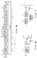
- a functional device comprising an output element 1 of a power metal oxide silicon FET (power MOSFET), circuit blocks 2, 3 and 4 for controlling the output element 1, and a Zener diode 5 for protecting a gate-to-source path of the output element 1, as shown in FIG. 3, a considerably high voltage has to be applied between the gate and source of the output element 1 in order to evaluate the withstand voltage of a gate oxide film of the output element 1.
- a power metal oxide silicon FET power MOSFET
- Zener diode 5 makes it difficult to apply such a high voltage between the gate and source of the output element 1. This drawback will be described in detail.
- the Zener diode 5 has a voltage of 10V enough to turn on the output element 1 in order to protect the gate-to-source path of the output element 1 from its breakage when a surge voltage higher than a predetermined value is applied between the gate and source of the output element 1.
- the gate oxide film of the power MOSFET has a time dependent dielectric breakdown (TDDB) mode in which the gate oxide film is broken in connection with time and temperature when a voltage is applied thereto for a long time, even though the voltage is lower than the breakdown voltage.
- TDDB time dependent dielectric breakdown
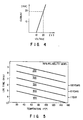
- FIG. 5 is a graph showing a relationship between a temperature and an estimated lifetime of the gate oxide film for each voltage to be used.
- a voltage of 20V has to be applied to the gate of the output element 1 for chip screening. Since, however, the Zener diode 5 for protecting the gate-to-source path of the output element 1 has a characteristic as shown in FIG. 4, if the voltage of 20V is applied, an overcurrent of nearly 20 mA flows through the Zener diode 5. The overcurrent causes the Zener diode 5 to be burnt and broken, and adversely affects the characteristic of the functional device.
- the present invention has been developed in consideration of the above situation, and its object is to provide a method of manufacturing a semiconductor device wherein the characteristics of power MOSFET output elements and circuit blocks connected to the output elements are evaluated before they are connected to serve as a functional device, which was difficult in the conventional semiconductor device, to thereby improve the reliability of a gate oxide film.
- IBM TECHNICAL DISCLOSURE BULLETIN, Vol. 13, No. 10, March 1971, page 2844 discloses a method to allow gate oxides of MOSFETS to be tested independently of their protective diodes.
- the diode In order to perform certain gate tests, the diode is disconnected firstly from its associated FET gate. After testing, a conductive spot is deposited to reconnect the diode and FET gate.
- a power MOSFET serving as one or more power output elements
- a Zener diode serving as a surge protection element for the power MOSFET
- a circuit block including an element for protecting a gate-to-source path of the power MOSFET for controlling the power MOSFET are formed on one chip
- the power MOSFET, Zener diode, and circuit block are connected to constitute a single functional device after an amount of withstand voltage of the gate of the power MOSFET is confirmed.
- connection of elements and circuit blocks is performed by metal wiring using aluminum electrodes.
- small signal elements 6 and 8 of small signal NPN transistors and a resistor 7, which serve as a control circuit block, a Zener diode 9 serving as a surge protection element, and a power MOSFET 10 serving as a power output element, are formed on one chip of a P-type semiconductor substrate P-Sub by a well-known technique, and surfaces of these elements are protected by an oxide film 3-1 formed thereon.
- contact holes are formed in the oxide film 3-1, and an aluminum electrode 3-2 is formed by evaporation as a first metal wiring layer.
- the elements are then connected to one another by the etching technique.
- the small signal elements 6 and 8 and the resistor 7 are connected to constitute a control circuit block 11.
- an insulation film 3-3 is formed, and openings 12-17 are formed therein as chip screening pads.
- the Zener diode 9 is not virtually connected between the gate and source of the power MOSFET 10.
- a probe of a die sorter (not shown) is applied to the bonding pads 12 and 13 to evaluate the control circuit block 11.
- the probe is applied to the bonding pads 14 and 16 to evaluate the Zener diode 9, and the probe is applied to the bonding pads 15, 16 and 17 to evaluate the power MOSFET 10 (including screening of a gate film).
- the control circuit block 11, Zener diode 9, and power MOSFET 10 are connected to one another by an aluminum electrode 3-4 (18).
- An insulation film 3-5 is then formed, and openings 12, 16 and 17 are formed as bonding pads, thereby obtaining a finished semiconductor functional device as shown in FIG. 2B.
- reference numerals 12 and 13 indicate an input terminal and an output terminal of the control circuit block 11, respectively
- numeral 14 denotes a cathode of the Zener diode 9
- numerals 15, 16, and 17 show a gate electrode, a source electrode, and a drain electrode of the power MOSFET 10, respectively.
- the semiconductor device comprises: at least one power output element 10 made of an insulated gate semiconductor element, a circuit element block 11 for controlling the power output element 10 and a surge protection element 9 for an input electrode of the power output element 10, the circuit element block 11, the power output element 10, and the surge protection element 9 being formed on a single semiconductor substrate;
- the characteristics of output elements e.g., power MOSFET
- circuit blocks can sufficiently be evaluated before they are connected to serve as a single function device, which was difficult in the conventional semiconductor device. Therefore, the reliability of the entire semiconductor device can be enhanced
- a surge protection diode is connected between the gate and source of the power MOSFET not when the first metal wiring layer is formed but when the second metal wiring layer is formed, screening of a gate film of the power MOSFET can be performed, without applying an overvoltage to the surge protection diode.
Landscapes
- Semiconductor Integrated Circuits (AREA)
- Metal-Oxide And Bipolar Metal-Oxide Semiconductor Integrated Circuits (AREA)
- Testing Or Measuring Of Semiconductors Or The Like (AREA)
Claims (4)
- Verfahren zur Herstellung einer Halbleitervorrichtung, welche mindestens ein Leistungsausgangselement (10) hat, bestehend aus einem Halbleiterelement mit isoliertem Gate, das Gate-, Drain- und Source-Gebiete hat, und einer Stoßschutzdiode (9), welche Kathoden- und Anoden-Gebiete hat, wobei das Leistungsausgangselement (10) und die Stoßschutzdiode beide auf einem Halbleitersubstrat (P-Sub) gebildet sind, wobei das Verfahren die Schritte umfasst:Bilden einer ersten Metallverdrahtungsschicht (3-2) zur Verbindung des Source-Gebiets des Leistungsausgangselements (10) und des Anoden- oder Kathoden-Gebiets der Stoßschutzdiode (9), und zur Bildung von Gate-, Drain- und Source-Elektroden (15, 17, 16) auf den Gate-, Drain- und Source-Gebieten des Leistungsausgangselements (10), und einer Kathoden- oder Anoden-Elektrode (14) auf dem Kathoden- oder Anoden-Gebiet der Stoßschutzdiode (9) ;Bewerten einer Haltespannung des Gate-Gebiets des Leistungsausgangselements (10) durch Anlegen einer vorbestimmten Spannung zwischen den Gate- und Source-Elektroden (15, 16) des Leistungsausgangselements (10); unddanach Bilden einer zweiten Metallverdrahtungsschicht (3-4) zur Verbindung der Gate-Elektrode (15) des Leistungsausgangselements (10) und der Kathoden- oder Anoden-Elektrode (14) der Stoßschutzdiode (9).
- Verfahren nach Anspruch 1, dadurch gekennzeichnet, dass:der erste Bildungsschritt weiterhin ein Schaltungselementblock zur Steuerung des Leistungsausgangselements (10) bildet, wobei die Stoßschutzdiode (9) und der Schaltungselementblock (11) auf dem gleichen Halbleitersubstrat (P-Sub) gebildet ist;der zweite Bildungsschritt weiterhin Felder (12, 13) bildet, die mit Eingangs- und Ausgangs-Anschlüssen des Schaltungaelementblocks (11) verbunden sind, durch Verwendung der ersten Metallverdrahtungsschicht (3-2);der Bewertungsschritt weiterhin den Schaltungselementblock (11) durch Verwendung der Felder (12, 13) bewertet; undder dritte Bildungsschritt weiterhin die Gate-Elektrode (15) des Leistungsausgangselements (10) und das mit dem Ausgangsanschluss des Schaltungselementblocks (11) verbundene Feld (13) verbindet, durch Verwendung der zweiten Metallverdrahtungsschicht (3-4).
- Verfahren nach Anspruch 1 oder 2, dadurch gekennzeichnet, dass das Leistungsausgangselement (10) ein Leistungs-MOSFET ist, und die Stoßschutzdiode (9) eine Zener-Diode ist.
- Verfahren nach einem der Ansprüche 1 bis 3, dadurch gekennzeichnet, dass der dritte Bildungsschritt weiterhin Felder (17, 16) bildet, die mit den Drain- und Source-Elektroden (17, 16) des Leistungsausgangselements (10) verbunden sind, durch Verwendung der zweiten Metallverdrahtungsschicht (3-4).
Applications Claiming Priority (3)
| Application Number | Priority Date | Filing Date | Title |
|---|---|---|---|
| JP293254/92 | 1992-10-30 | ||
| JP4293254A JPH06151737A (ja) | 1992-10-30 | 1992-10-30 | 半導体装置及びその製造方法 |
| JP29325492 | 1992-10-30 |
Publications (2)
| Publication Number | Publication Date |
|---|---|
| EP0595355A1 EP0595355A1 (de) | 1994-05-04 |
| EP0595355B1 true EP0595355B1 (de) | 2001-06-06 |
Family
ID=17792449
Family Applications (1)
| Application Number | Title | Priority Date | Filing Date |
|---|---|---|---|
| EP93117610A Expired - Lifetime EP0595355B1 (de) | 1992-10-30 | 1993-10-29 | Halbleiteranordnung mit einem Schutzelement und Verfahren zu ihrer Herstellung |
Country Status (5)
| Country | Link |
|---|---|
| US (1) | US5418383A (de) |
| EP (1) | EP0595355B1 (de) |
| JP (1) | JPH06151737A (de) |
| KR (1) | KR970003890B1 (de) |
| DE (1) | DE69330303T2 (de) |
Families Citing this family (9)
| Publication number | Priority date | Publication date | Assignee | Title |
|---|---|---|---|---|
| JP3226074B2 (ja) | 1994-02-17 | 2001-11-05 | 富士電機株式会社 | 半導体集積回路装置 |
| EP0696054B1 (de) * | 1994-07-04 | 2002-02-20 | STMicroelectronics S.r.l. | Verfahren zur Herstellung von Leistungsbauteilen hoher Dichte in MOS-Technologie |
| US5610425A (en) * | 1995-02-06 | 1997-03-11 | Motorola, Inc. | Input/output electrostatic discharge protection circuit for an integrated circuit |
| JP3386943B2 (ja) * | 1995-10-30 | 2003-03-17 | 三菱電機株式会社 | 半導体装置 |
| EP0773588B1 (de) * | 1995-11-10 | 2002-06-19 | Consorzio per la Ricerca sulla Microelettronica nel Mezzogiorno - CoRiMMe | Integriertes MOS-Bauelement mit einer Gateschutzdiode |
| US5602046A (en) * | 1996-04-12 | 1997-02-11 | National Semiconductor Corporation | Integrated zener diode protection structures and fabrication methods for DMOS power devices |
| SE513283C2 (sv) * | 1996-07-26 | 2000-08-14 | Ericsson Telefon Ab L M | MOS-transistorstruktur med utsträckt driftregion |
| US5844282A (en) * | 1997-03-28 | 1998-12-01 | Nec Corporation | Semiconductor device having field effect transistor connected at gate electrode to protective junction diode discharging in the presence of light |
| US8476709B2 (en) | 2006-08-24 | 2013-07-02 | Infineon Technologies Ag | ESD protection device and method |
Family Cites Families (6)
| Publication number | Priority date | Publication date | Assignee | Title |
|---|---|---|---|---|
| US3999212A (en) * | 1967-03-03 | 1976-12-21 | Hitachi, Ltd. | Field effect semiconductor device having a protective diode |
| US3585712A (en) * | 1968-12-12 | 1971-06-22 | Trw Semiconductors Inc | Selection and interconnection of devices of a multidevice wafer |
| JPS582453B2 (ja) * | 1975-02-28 | 1983-01-17 | 日本電気株式会社 | ダイキボハンドウタイシユウセキカイロソウチ |
| US4479088A (en) * | 1981-01-16 | 1984-10-23 | Burroughs Corporation | Wafer including test lead connected to ground for testing networks thereon |
| JPH081956B2 (ja) * | 1987-11-06 | 1996-01-10 | 日産自動車株式会社 | 保護機能を備えた縦型mosfet |
| US4814283A (en) * | 1988-04-08 | 1989-03-21 | General Electric Company | Simple automated discretionary bonding of multiple parallel elements |
-
1992
- 1992-10-30 JP JP4293254A patent/JPH06151737A/ja active Pending
-
1993
- 1993-10-29 KR KR93022706A patent/KR970003890B1/ko not_active Expired - Fee Related
- 1993-10-29 DE DE69330303T patent/DE69330303T2/de not_active Expired - Lifetime
- 1993-10-29 US US08/143,060 patent/US5418383A/en not_active Expired - Lifetime
- 1993-10-29 EP EP93117610A patent/EP0595355B1/de not_active Expired - Lifetime
Also Published As
| Publication number | Publication date |
|---|---|
| EP0595355A1 (de) | 1994-05-04 |
| US5418383A (en) | 1995-05-23 |
| JPH06151737A (ja) | 1994-05-31 |
| DE69330303T2 (de) | 2001-10-31 |
| DE69330303D1 (de) | 2001-07-12 |
| KR970003890B1 (en) | 1997-03-22 |
Similar Documents
| Publication | Publication Date | Title |
|---|---|---|
| KR100731270B1 (ko) | 테스트 가능한 정전기 방전 보호 회로 | |
| US5889308A (en) | Semiconductor device having an electrostatic discharging protection circuit using a non-ohmic material | |
| US4994904A (en) | MOSFET having drain voltage detection function | |
| US7482861B1 (en) | Semiconductor integrated circuit device, and method of manufacturing the same | |
| TW583761B (en) | ESD protection for a CMOS output stage | |
| CA1068008A (en) | Mos input protection structure | |
| EP0215493B1 (de) | Geschützte MOS-Transistorschaltung | |
| US5581432A (en) | Clamp circuit and method for identifying a safe operating area | |
| EP0595355B1 (de) | Halbleiteranordnung mit einem Schutzelement und Verfahren zu ihrer Herstellung | |
| JP3353388B2 (ja) | 電力用半導体装置 | |
| US5381105A (en) | Method of testing a semiconductor device having a first circuit electrically isolated from a second circuit | |
| JP3369391B2 (ja) | 誘電体分離型半導体装置 | |
| US5828081A (en) | Integrated semiconductor device | |
| US5654863A (en) | Integrated circuit having a gate oxide | |
| US5923048A (en) | Semiconductor integrated circuit device with test element | |
| CN101582421B (zh) | 可测试静电放电保护电路 | |
| EP0431586B1 (de) | Hochleistungshalbleiterbauelement | |
| US6760204B2 (en) | Semiconductor integrated circuit device and method for designing the same | |
| US20040056339A1 (en) | Semiconductor component with ESD protection | |
| JPH01222624A (ja) | モノリシック過電圧保護集合体 | |
| US5565692A (en) | Insulated gate transistor electrostatic charge protection | |
| JP2776569B2 (ja) | 半導体装置 | |
| JPS63239972A (ja) | 半導体装置の入力保護回路 | |
| JPH0462943A (ja) | 半導体装置 | |
| JPH04305937A (ja) | 半導体装置およびその製造方法 |
Legal Events
| Date | Code | Title | Description |
|---|---|---|---|
| PUAI | Public reference made under article 153(3) epc to a published international application that has entered the european phase |
Free format text: ORIGINAL CODE: 0009012 |
|
| 17P | Request for examination filed |
Effective date: 19931029 |
|
| AK | Designated contracting states |
Kind code of ref document: A1 Designated state(s): DE FR IT |
|
| 17Q | First examination report despatched |
Effective date: 19960521 |
|
| GRAG | Despatch of communication of intention to grant |
Free format text: ORIGINAL CODE: EPIDOS AGRA |
|
| GRAG | Despatch of communication of intention to grant |
Free format text: ORIGINAL CODE: EPIDOS AGRA |
|
| GRAH | Despatch of communication of intention to grant a patent |
Free format text: ORIGINAL CODE: EPIDOS IGRA |
|
| GRAH | Despatch of communication of intention to grant a patent |
Free format text: ORIGINAL CODE: EPIDOS IGRA |
|
| GRAA | (expected) grant |
Free format text: ORIGINAL CODE: 0009210 |
|
| AK | Designated contracting states |
Kind code of ref document: B1 Designated state(s): DE FR IT |
|
| ITF | It: translation for a ep patent filed | ||
| REF | Corresponds to: |
Ref document number: 69330303 Country of ref document: DE Date of ref document: 20010712 |
|
| ET | Fr: translation filed | ||
| PLBE | No opposition filed within time limit |
Free format text: ORIGINAL CODE: 0009261 |
|
| STAA | Information on the status of an ep patent application or granted ep patent |
Free format text: STATUS: NO OPPOSITION FILED WITHIN TIME LIMIT |
|
| 26N | No opposition filed | ||
| PGFP | Annual fee paid to national office [announced via postgrant information from national office to epo] |
Ref country code: IT Payment date: 20071026 Year of fee payment: 15 |
|
| PG25 | Lapsed in a contracting state [announced via postgrant information from national office to epo] |
Ref country code: IT Free format text: LAPSE BECAUSE OF NON-PAYMENT OF DUE FEES Effective date: 20081029 |
|
| PGFP | Annual fee paid to national office [announced via postgrant information from national office to epo] |
Ref country code: DE Payment date: 20101027 Year of fee payment: 18 |
|
| PGFP | Annual fee paid to national office [announced via postgrant information from national office to epo] |
Ref country code: FR Payment date: 20111103 Year of fee payment: 19 |
|
| REG | Reference to a national code |
Ref country code: FR Ref legal event code: ST Effective date: 20130628 |
|
| PG25 | Lapsed in a contracting state [announced via postgrant information from national office to epo] |
Ref country code: DE Free format text: LAPSE BECAUSE OF NON-PAYMENT OF DUE FEES Effective date: 20130501 |
|
| REG | Reference to a national code |
Ref country code: DE Ref legal event code: R119 Ref document number: 69330303 Country of ref document: DE Effective date: 20130501 |
|
| PG25 | Lapsed in a contracting state [announced via postgrant information from national office to epo] |
Ref country code: FR Free format text: LAPSE BECAUSE OF NON-PAYMENT OF DUE FEES Effective date: 20121031 |