EP0595632A2 - Circuits de synchronisation de phase - Google Patents
Circuits de synchronisation de phase Download PDFInfo
- Publication number
- EP0595632A2 EP0595632A2 EP93308593A EP93308593A EP0595632A2 EP 0595632 A2 EP0595632 A2 EP 0595632A2 EP 93308593 A EP93308593 A EP 93308593A EP 93308593 A EP93308593 A EP 93308593A EP 0595632 A2 EP0595632 A2 EP 0595632A2
- Authority
- EP
- European Patent Office
- Prior art keywords
- voltage
- current
- signal
- phase
- input
- Prior art date
- Legal status (The legal status is an assumption and is not a legal conclusion. Google has not performed a legal analysis and makes no representation as to the accuracy of the status listed.)
- Granted
Links
Images







Classifications
-
- H—ELECTRICITY
- H03—ELECTRONIC CIRCUITRY
- H03L—AUTOMATIC CONTROL, STARTING, SYNCHRONISATION OR STABILISATION OF GENERATORS OF ELECTRONIC OSCILLATIONS OR PULSES
- H03L7/00—Automatic control of frequency or phase; Synchronisation
- H03L7/06—Automatic control of frequency or phase; Synchronisation using a reference signal applied to a frequency- or phase-locked loop
- H03L7/08—Details of the phase-locked loop
- H03L7/085—Details of the phase-locked loop concerning mainly the frequency- or phase-detection arrangement including the filtering or amplification of its output signal
- H03L7/093—Details of the phase-locked loop concerning mainly the frequency- or phase-detection arrangement including the filtering or amplification of its output signal using special filtering or amplification characteristics in the loop
-
- H—ELECTRICITY
- H03—ELECTRONIC CIRCUITRY
- H03L—AUTOMATIC CONTROL, STARTING, SYNCHRONISATION OR STABILISATION OF GENERATORS OF ELECTRONIC OSCILLATIONS OR PULSES
- H03L7/00—Automatic control of frequency or phase; Synchronisation
- H03L7/06—Automatic control of frequency or phase; Synchronisation using a reference signal applied to a frequency- or phase-locked loop
- H03L7/08—Details of the phase-locked loop
- H03L7/10—Details of the phase-locked loop for assuring initial synchronisation or for broadening the capture range
- H03L7/107—Details of the phase-locked loop for assuring initial synchronisation or for broadening the capture range using a variable transfer function for the loop, e.g. low pass filter having a variable bandwidth
- H03L7/1072—Details of the phase-locked loop for assuring initial synchronisation or for broadening the capture range using a variable transfer function for the loop, e.g. low pass filter having a variable bandwidth by changing characteristics of the charge pump, e.g. changing the gain
-
- H—ELECTRICITY
- H03—ELECTRONIC CIRCUITRY
- H03L—AUTOMATIC CONTROL, STARTING, SYNCHRONISATION OR STABILISATION OF GENERATORS OF ELECTRONIC OSCILLATIONS OR PULSES
- H03L2207/00—Indexing scheme relating to automatic control of frequency or phase and to synchronisation
- H03L2207/04—Modifications for maintaining constant the phase-locked loop damping factor when other loop parameters change
Definitions
- the present invention relates to phase synchronization circuits used for generating a clock signal from an input signal.
- phase synchronization circuits have been used to generate a clock signal from an input signal.
- a clock signal is generated, by using such a phase synchronization circuit, from an input data signal read by a magnetic head in a magnetic disk drive.
- the phase synchronization circuit is comprised of a phase comparator, a loop-filter, and a VCO (voltage-controlled oscillator).
- the phase comparator compares the phase of an output signal of the VCO with that of an input signal.
- An output signal of the phase comparator is provided to the loop filter, which provides a control voltage to the VCO.
- the loop filter may have various structures depending on the arrangement of the phase comparator.
- the charge pump circuit controls the charging and discharging of the capacitor in response to an output signal of the phase comparator whose pulse width corresponds to a phase difference between the output signal of the VCO and the input signal.
- a charge voltage on the capacitor serves as the control voltage for the VCO. Since this control voltage controls the phase (frequency) of the output signal of the VCO, the phase of the output signal of the VCO is synchronized with that of the input signal.
- the input signal is formed, for example, by reading a magnetic disk with a head of a magnetic disk drive and by shaping the read signal according to zero-crossing points and peaks of the signal.
- the VCO provides a clock signal whose phase is in synchronization with that of the input signal. According to the clock signal, the signal read through the head is processed to reproduce data.
- some magnetic disk drives employ a zone bit recording method that arranges more sectors in outer tracks than in inner tracks to increase storage capacity. According to this method, the clock frequency used when accessing inner tracks differs from that used when accessing outer tracks.
- the frequency of an input signal may fluctuate, and the output signal of the VCO must follow such fluctuations. Accordingly, the charge pump circuit may change the charging or discharging current of the capacitor. This results in changing the damping factor of the phase synchronization loop, and this destabilizes the phase synchronization operation.
- phase synchronization circuit In order to generate a stabilized clock signal with such fluctuating clock frequencies, it is necessary for the phase synchronization circuit to provide a plurality of loop filters for the different frequencies, and selects a suitable loop filter by switching in accordance with the frequency. This may cause the construction of the phase synchronization circuit to be complicated and increase the cost of the circuit.
- phase synchronization circuit that can realize phase synchronization without changing the damping factor even if the frequency of an input signal fluctuates.
- An embodiment of the present invention can provide a phase synchronization circuit having a voltage-controlled oscillator, a phase comparator for comparing the phase of an input signal with that of an output signal of the voltage-controlled oscillator, and a loop filter for receiving an output signal of the phase comparator and providing a control voltage to the voltage-controlled oscillator.
- the loop filter has a first voltage-current converter for receiving the output signal of the phase comparator, a second voltage-current converter for receiving an output signal of the first voltage-current converter, a capacitor connected between input and output terminals of the first voltage-current converter, and a resistor for converting an output signal of the second voltage-current converter into the control voltage for the voltage-controlled oscillator.
- the phase synchronization circuit may have a distributor for changing, according to a cut-off frequency, the ratio between control currents supplied from a reference current source to input and output stages of a current multiplier of each of the first and second voltage-current converters.
- the phase synchronization circuit may have a distributor for changing, according to a cut-off frequency, the ratio between control currents that are supplied from a reference current source to input and output stages of a current multiplier of each of the first and second voltage-current converters, and an adder disposed between the loop filter and the VCO, to change the center frequency of the VCO according to the cut-off frequency.
- the phase synchronization circuit may have a structure for changing, according to a cut-off frequency, the ratio between control currents supplied from a reference current source and distributed by a distributor to current multipliers of the first and second voltage-current converters, a center frequency controlling offset voltage applied to an adder disposed between the loop filter and the VCO, and a current supplied to a charge pump circuit connected between the phase comparator and the loop filter.
- the phase synchronization circuit may have a first distributor for changing, according to a cut-off frequency, the ratio between control currents that are supplied from a reference current source to input and output stages of a current multiplier of each of the first and second voltage-current converters, and a second distributor for changing the ratio between the control currents supplied to the input and output stages of each of the current multipliers, to shorten the acquisition time when the frequency of the input signal is changed.
- Each of the first and second voltage-current converters for converting an input voltage into a current preferably has a current multiplier.
- the first voltage-current converter converts an output signal from the phase comparator into a current to charge and discharge the capacitor connected between the input and output terminals of the first voltage-current converter.
- the second voltage-current converter converts a charge voltage of a capacitor into a current.
- a voltage corresponding to the product of the current and the resistance of the resistor is the control voltage that controls the VCO.
- a control terminal provides a control signal in response to a change in the frequency of the input signal. According to the control signal, the transconductances of the voltage-current converters are changed to change the control voltage for the VCO, thereby changing the frequency of the output signal of the VCO.
- the transconductances are changed by changing the ratio between the control currents supplied to the input and output stages of each of the voltage-current converters without changing a damping factor.
- the control currents to the current multipliers of the first and second voltage-current converters are supplied from the reference current source.
- the distributor changes the ratio between the control currents supplied to the input and output stages, so that the ratio maintains a predetermined value even if the source voltage and temperature fluctuate.
- the center frequency of the VCO may be changed by adding an offset voltage. This results in adjusting the frequency of the output signal of the VCO to the frequency of the input signal that may fluctuate, thereby improving the phase synchronization speed of the phase synchronization loop.
- the current to the charge pump circuit may be changed to change the charge voltage of the capacitor. This results in changing the control voltage to the VCO.
- the ratio between the control currents supplied to the input and output stages of the current multiplier of each of the first and second voltage-current converters may be changed to change the control voltage to the VCO.
- An offset voltage may be added to the output voltage of the loop filter, to change the control voltage to the VCO.
- the control current to the input stages of the current multipliers of the first and second voltage-current converters may be increased to increase the transconductance and shorten the acquisition time.
- the transconductance may be temporarily increased when the ratio between the control currents to the input and output stages of each of the current multipliers is changed according to a cut-off frequency, to shorten an acquisition time.
- the first and second distributors are controlled to change the ratio between the control currents to the input and output stages of each of the current multipliers according to the cut-off frequency, to thereby speedily adjust the frequency of the output signal of the VCO.
- a phase comparator 42 compares the phase of an output signal of a voltage-controlled oscillator (VCO) 41 with that of an input signal.
- the phase comparator 42 outputs pulse-width-modulated signal in accordance with a phase difference between the output signal of the VCO and the input signal.
- the output signal of the phase comparator 42 is input to a loop filter 43, which provides a control voltage to the VCO 41.
- the loop filter 43 may have various structures depending on the arrangement of the phase comparator 42.
- the loop filter of this example has a charge pump circuit 44 for changing the input pulse-width-modulated signal into a voltage, a capacitor 45, and a resistor 46.
- the capacitor 45 and the resistor 46 are connected in series between an output terminal of the charge pump circuit 44 and ground.
- the construction of the charge pump circuit 44 per se is well-known, so that a disclosure thereof is omitted.
- the charge pump circuit 44 controls the charging and discharging of the capacitor 45 in response to an output signal from the phase comparator 42 whose pulse width corresponds to a phase difference between the output signal of the VCO 41 and the input signal.
- a charge voltage on the capacitor 45 serves as the control voltage for the VCO 41. Since this control voltage controls the phase (frequency) of the output signal of the VCO 41, the phase of the output signal of the VCO 41 is synchronized with that of the input signal.
- the input signal is formed, for example, by reading a magnetic disk with a head of a magnetic disk drive and by shaping the read signal according to the zero-crossing points and peaks of the signal.
- the VCO 41 provides a clock signal whose phase is in synchronization with that of the input signal. According to the clock signal, the signal read through the head is processed to reproduce data.
- the frequency of an input signal may fluctuate, and the output signal of the VCO 41 must follow such fluctuations.
- the reason why such fluctuations occur is that a frequency of the data read from an inner track of the disk and a frequency of the data read from an inner track of the disk are different, since the outer track area and the inner track area on the magnetic disk involve different numbers of sectors in the magnetic disk drive employing the zone bit recording method.
- the charge pump circuit 44 should change the charging or discharging current of the capacitor 45, since a cut-off frequency and the center frequency of the VCO 41 depends on the frequency of the input data. This results in changing the damping factor of the phase synchronization loop, and this destabilizes the phase synchronization operation.
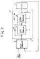
- FIG. 2 is a block circuit diagram showing parts of a phase synchronization circuit embodying the present invention.
- the phase synchronization circuit includes a VCO (voltage-controlled oscillator) 11, a phase comparator 12 for comparing the phase of an input signal with that of an output signal of the VCO 11, and a loop filter 13 for receiving an output signal of the phase comparator and providing a control voltage for the VCO 11.
- the loop filter 13 has a first voltage-current converter 14 for receiving the output signal of the phase comparator 12, a second voltage-current converter 15 for receiving an output signal of the first voltage-current converter 14, a capacitor 16 connected between input and output terminals of the first voltage-current converter 14, and a resistor 17 for converting an output signal of the second voltage-current converter 15 into the control voltage for the VCO 11.
- the loop filter 13 has a control terminal 8 for receiving a control signal to control the first and the second voltage-current converter 14 and 15.
- Figure 3 explains a first embodiment of the present invention.
- Numeral 11 is a VCO
- 12 is a phase comparator
- 13 is a loop filter
- 14 and 15 are first and second voltage-current converters
- 16 is a capacitor
- 17 is a resistor
- 18 is a distributor.
- the first and the second voltage-current converters 14 and 15 have a control terminal CIe and CIm respectively.
- a control current I is input to each control terminal CIe
- a control current I' is input to each control terminal CIm.
- the control current I' is generated by the distributor 18.
- the distributor 18 changes the ratio between a control current I and a control current I' according to a cut-off frequency control signal cf.
- Figure 4 shows an example of the current multiplier employed in each of the voltage-current converters 14 and 15.
- Reference marks D1 and D2 are diodes, Q1 to Q4 are transistors, R1 is a resistor having a resistance of 2Re ⁇ , CIe and CIm are control terminals, and Ie, Im, and 2Im are currents from constant current sources Ie1, Ie2, Im1, Im2, and Im3.
- the resistance 2Re means that there are series-connected two resistors having a resistance of Re.
- the voltage-current converters 14 and 15 is comprised of input stages including the diodes D1 and D2, the transistors Q1 and Q2, the resister R1, and two current sources Ie1 and Ie2, and output stages including the transistors Q3 and Q4, and three current sources Im1, Im2, and Im3.
- the distributor 18 in Fig. 3 changes the ratio between a control current I for input stages and a control current I' for output stages of the current multipliers of the voltage-current converters 14 and 15 according to a cut-off frequency control signal cf.
- the current Ie for the input stage is controlled according to the control current I from the control terminal CIe
- the current Im for the output stage is controlled according to the control current I' from the control terminal CIm.
- Reference marks Vccl and Vcc2 in Fig. 4 are source voltages, Vin is an input voltage, and io is an output current.
- the transistors Q1 and Q2 form the input stage of the current multiplier, and the transistors Q3 and Q4 form the output stage thereof.
- the output current io of the first voltage-current converter 14 is applied to the capacitor 16 as shown in Fig. 3.
- a charge voltage of the capacitor 16 is the input voltage Vin to the second voltage-current converter 15.
- the output current io of the second voltage-current converter 15 is applied to the resistor 17, which provides the control voltage for the VCO 11.
- Each of the transistors Q1 to Q4 in Fig. 4 has a voltage gain of 1 and an emitter resistance of re ⁇ .
- the resistor R1 is selected to be re ⁇ Re and is connected between emitters of the transistors Q1 and Q2.
- collector currents of the transistors Q1 and Q2 are Ic1 and Ic2, respectively
- the current I from a reference current source (not shown) is supplied to the control terminal CIe to control the current Ie to the input stage of the current multiplier of each of the first and second voltage-current converters 14 and 15.
- This control current I is divided and is passed through the distributor 18 to provide the control current I'.
- the control current I' is supplied to the control terminal CIm to control the current Im for the output stage of the current multiplier of each of the first and second voltage-current converters 14 and 15.
- the distributor 18 is controlled according to the cut-off frequency control signal cf, to change the control current I'.
- the control current Im is changed to change the transconductance gm, to thereby change the control voltage for the VCO 11. Consequently, the frequency of the output signal of the VCO 11 quickly follows a change in the cut-off frequency.
- H(s) [KdKvgmR ⁇ S+(gm/C) ⁇ ]/[S2+KdKvgmR ⁇ S+(gm/C) ⁇ ]
- ⁇ n (KdKvR/C) 1/2
- gm ⁇ (KdKvRC) 1/2 ⁇ 2
- the loop filter 13 employing the voltage-current converters 14 and 15 is capable of maintaining the damping factor ⁇ without regard to the frequency of the input signal.
- the control signal cf controls the distributor 18 to change the ratio of the current Im to the current Ie, thereby changing the transconductance gm of the voltage-current converters 14 and 15 and synchronizing the frequency of the output signal from the VCO 11 with the frequency of the input signal.
- the damping factor ⁇ is unchanged to stabilize the phase synchronization. Since the currents Ie and Im are obtained from the control current I from the reference current source, the ratio between the currents Ie and Im is maintained even if the source voltage and temperature fluctuate, to stabilize the phase synchronization.
- Figure 5 explains a second embodiment of the present invention.
- Numeral 19 is a cut-off frequency conversion table
- 20 is a center frequency conversion table
- 21 is an adder.
- the same reference marks as those of Fig. 2 represent the same parts.
- the second embodiment is applicable for generating a clock signal in a magnetic disk drive employing the zone bit recording method.
- Head position data tr indicating the position of a head on a magnetic disk is supplied to the cut-off frequency conversion table 19 and center frequency conversion table 20.
- An outer track area and an inner track area on the magnetic disk involve different numbers of sectors.
- a cut-off frequency and the center frequency of the VCO 11 are determined.
- a current I from the reference current source forms a control current Ie for the input stage of the current multiplier of each of the first and second voltage-current converters 14 and 15.
- the current I is supplied to the distributor 18, which provides a control current I' supplied to the control terminal CIm.
- the current Im for the output stage of the current multiplier of each of the first and second voltage-current converters 14 and 15 is controlled by the control current I'.
- the cut-off frequency conversion table 19 provides a control signal cf to the distributor 18, to decrease the control current Im
- the center frequency conversion table 20 provides an offset voltage to the adder 21, to increase the center frequency of the VCO 11.
- the change in the center frequency by the offset voltage and the change in the transconductance gm of the loop filter 13 simultaneously occur, to quickly synchronize the phase of the output signal of the VCO 11 with the phase of the input signal whose frequency has been increased.
- an offset voltage is applied to the adder 21 to decrease the center frequency of the VCO 11.
- the control current from the distributor 18 is increased to decrease the transconductance gm of the loop filter 13.
- the frequency of the output signal of the VCO 11 is quickly synchronized with the changed frequency of the input signal.
- Figure 6 explains a third embodiment of the present invention.
- Numeral 20 is a center frequency control table
- 24 is a charge pump circuit
- 25 is a capacitor.
- the same reference marks as those of Fig. 4 represent the same parts.
- the phase comparator 12 outputs pulse-width-modulated signal in accordance with a phase difference between the output signal of the VCO 11 and the input signal similar to the conventional phase comparator 42 as explained in Fig. 1.
- the output signal from the phase comparator 12 includes an up-signal and down-signal in accordance with the phase lead and phase lag.
- the charge pump circuit 24 and the capacitor 25 change the pulse-width-modulated signal into a voltage.
- the charge pump circuit 24 controls the charging and discharging of the capacitor 25 according to a phase difference, which is provided by the phase comparator 12 as a difference between an output signal of the VCO 11 and an input signal.
- a charge voltage of the capacitor 25 is an input voltage to the loop filter 13.
- the center frequency control table 20 controls the current to the charge pump circuit 24 as well as an offset voltage to the adder 21. Namely, the current to the charge pump circuit 24 is changed depending on whether a head is positioned in an outer track area or in an inner track area of a magnetic disk. For example, when the head is in the outer track area, the clock frequency increases, so that the current to the charge pump circuit 24 is increased and the offset voltage to the adder 21 is changed to increase the center frequency of the VCO 11.
- the cut-off frequency conversion table 19 controls the distributor 18, to change the current Im for the output stage of the current multiplier of each of the first and second voltage-current converters 14 and 15, to thereby change the transconductance gm of the converters.
- the VCO 11 quickly generates a clock signal having a new frequency.
- Figure 7 explains a fourth embodiment of the present invention.
- the same reference marks as those of Fig. 2 represent the same parts.
- Numeral 18 is a first distributor to supply a control current 11 to the control terminal CIe of the first and the second voltage-current converters 14 and 15.
- Numeral 22 is a second distributor to supply a control current I2 to the control terminal CIm of the first and the second voltage-current converters 14 and 15.
- the first and second voltage-current converters 14 and 15 are formed in an integrated circuit 26.
- the capacitor 16 and resistor 17 are externally connected to the integrated circuit 26.
- a cut-off frequency control signal cf controls the first distributor 18 to produce a control current 11 from the current I provided by the reference current source.
- a acquisition time control signal fnt controls the second distributor 22 to produce a control current I2 from the current I provided by the reference current source.
- the control signal fnt increases the control current I2 when a cut-off frequency is changed, to increase the ratio between the currents Ie and Im as shown in Fig. 4. This results in increasing the transconductance gm of the converters 14 and 15, to shorten an acquisition time. After the phase synchronization is completed, the control current I2 returns to the original value.
- the distributor 18 changes the control current 11.
- a clock frequency changes.
- the control signal fnt is provided for a predetermined duration, and the control signal cf indicating the magnitude of the clock frequency is produced.
- These control signals control the first and second distributors 18 and 22 to change the distribution ratio of the current I provided by the reference current source, to thereby quickly achieve phase synchronization in response to the frequency change in the input signal.
- the first and second voltage-current converters 14 and 15 are easily integrated into the integrated circuit 26 with the capacitor 16 and resistor 17 being externally connected thereto.
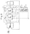
- Figure 8 explains a fifth embodiment of the present invention.
- the same reference marks as those of Fig. 7 represent the same parts.
- the first and second distributors 18 and 22 are connected in series.
- the cut-off frequency control signal cf is used to control the first distributor 18, and the acquisition time control signal fnt is used to control the second distributor 22, similar to the embodiment of Fig. 7.
- the first and second distributors 18 and 22 control the current Im for the output stage of the current multiplier of each of the first and second voltage-current converters 14 and 15, to change the ratio of the control current I' to the input control current I, to thereby change the transconductance gm of the converters 14 and 15.
- the transconductance gm is adjusted according to the frequency of an input signal.
- the transconductance gm is adjusted to shorten an acquisition time whenever the frequency of the input signal is changed.
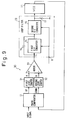
- Figure 9 explains a sixth embodiment of the present invention.
- the phase comparator 12 outputs pulse-width-modulated signal in accordance with a phase difference between the output signal of the VCO 11 and the input signal, similar to the conventional phase comparator 42 and the phase comparator 12 as explained in Figs. 1 and 6.
- the output signal from the phase comparator 12 includes an up-signal and down-signal in accordance with the phase lead and phase lag.
- the up-signal is output from the phase comparator 12 when the phase of the input signal to the phase comparator 12 is leading to the phase of the output signal from the VCO 11.
- the up-signal increases the frequency of the VCO 11.
- the down-signal is output from the phase comparator 12 when the phase of the input signal to the phase comparator 12 is lagging to the phase of the output signal from the VCO 11.
- a converting circuit 30 between the phase comparator 12 and the loop filter 13 to change the pulse-width-modulated signal from the phase comparator 12 into a voltage for inputting the same to the loop filter.
- the converting circuit 30 includes a first level shaper 31, a second level shaper 32, and an adder 33.
- the second level shaper 32 shapes an input down-signal into a voltage signal having a constant level of Vo, when the the phase comparator 12 detects the phase lag.
- the adder 33 calculates the difference between the input signals at a positive input terminal "+" and a negative input terminal "-".
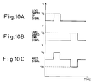
- Figure 10A shows the wave form of a level-shaped up-signal output from the first level shaper 31 at point A in Fig. 9.
- Figure 10B shows the wave form of a level-shaped down-signal output from the second level shaper 32 at point B in Fig. 9.
- Figure 10C shows the wave form of an added signal at point C in Fig. 9.
- Figure 11 shows an concrete example of the first level shaper 31, the second level shaper 32, and the adder 33 in Fig. 9.
- Reference marks Q5 to Q14 are transistors, R2, R3, R4, and R6 are resistors having resistance of R, R, r, r, and 2r ⁇ respectively, and I1 to I8 are constant current sources.
- the first level shaper 31 is comprised of three transistors Q5 to Q7, a resistor R2 having a resistance R ⁇ , and two current sources I1 and I2.
- the second level shaper 32 is comprised of three transistors Q8 to Q10, a resister R3 having a resistance R ⁇ , and two current sources I3 and I4.
- the adder 33 is comprised of four transistors Q11 to Q14, three resistors R4, R5, and R6 having a resistance r, r, and 2r ⁇ respectively, and four current sources I5 to I8.
- the transistor 05 turns on when the up-signal is input to the base thereof, and a current I1 flows through the resistor R2, thereby a voltage level of a base of the transistor Q7 decreases by R*I1 volts.
- an output voltage from the first level shaper 31 will be (Vcc-R*I1-V BE ).
- an output voltage from the first level shaper 31 will be (Vcc-V BE ).
- the operation of the second level shaper 32 is the same as that of the first level shapter 31, so that the operation thereof will be omitted.
- the adder 33 calculates a difference between the level-shaped up-signal and the level-shaped down-signal.
- the first and the second level shaper 31 and 32, and the adder 33 can be formed in an integrated circuit as a differential amplifier 34 as shown in Fig. 12.
- the differential amplifier 34 is comprised of four transistors Q15 to Q18, three resistors R7, R8, and R9 having a resistance of R, R, and 2R1 ⁇ respectively, and four current sources I9 to I12.
- Figure 13 explains a seventh embodiment of the present invention.
- the above-described converting circuit 30 including the first level shaper 31, the second level shaper 32, and the adder 33 is inserted between the phase comparator 12 and the loop filter 13 of the phase synchronization circuit shown in Fig. 3.
- Figure 14 explains a eighth embodiment of the present invention.
- the above-described converting circuit 30 including the first level shaper 31, the second level shaper 32, and the adder 33 is inserted between the phase comparator 12 and the loop filter 13 of the phase synchronization circuit shown in Fig. 5.
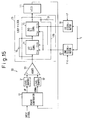
- Figure 15 explains a ninth embodiment of the present invention.
- the above-described converting circuit 30 including the first level shaper 31, the second level shaper 32, and the adder 33 is inserted between the phase comparator 12 and the loop filter 13 of the phase synchronization circuit shown in Fig. 7.
- Figure 16 explains a tenth embodiment of the present invention.
- the above-described converting circuit 30 including the first level shaper 31, the second level shaper 32, and the adder 33 is inserted between the phase comparator 12 and the loop filter 13 of the phase synchronization circuit shown in Fig. 8.
- the present invention is not limited to the above embodiments.
- Various modifications to the present invention are possible.
- the capacitor 16 may be connected between input and output terminals of the second voltage-current converter 15, and the resistor 17 may be connected between output terminal and ground.
- This modification is shown as an eleventh embodiment of the present invention in Fig. 17. This modification can be applied to every embodiment described above.
- the frequency of an input signal is changed in two stages.
- the frequency may be changed in multiple stages.
- the control currents I and I' for the voltage-current converters 14 and 15 are changed to carry out phase synchronization according to the frequency of the input signal.
Landscapes
- Stabilization Of Oscillater, Synchronisation, Frequency Synthesizers (AREA)
Applications Claiming Priority (2)
| Application Number | Priority Date | Filing Date | Title |
|---|---|---|---|
| JP4289773A JP2613532B2 (ja) | 1992-10-28 | 1992-10-28 | 位相同期回路 |
| JP289773/92 | 1992-10-28 |
Publications (3)
| Publication Number | Publication Date |
|---|---|
| EP0595632A2 true EP0595632A2 (fr) | 1994-05-04 |
| EP0595632A3 EP0595632A3 (fr) | 1994-12-21 |
| EP0595632B1 EP0595632B1 (fr) | 1998-01-07 |
Family
ID=17747580
Family Applications (1)
| Application Number | Title | Priority Date | Filing Date |
|---|---|---|---|
| EP93308593A Expired - Lifetime EP0595632B1 (fr) | 1992-10-28 | 1993-10-28 | Circuits de synchronisation de phase |
Country Status (4)
| Country | Link |
|---|---|
| US (1) | US5373257A (fr) |
| EP (1) | EP0595632B1 (fr) |
| JP (1) | JP2613532B2 (fr) |
| DE (1) | DE69316157T2 (fr) |
Cited By (6)
| Publication number | Priority date | Publication date | Assignee | Title |
|---|---|---|---|---|
| EP0731565A1 (fr) * | 1995-03-07 | 1996-09-11 | STMicroelectronics S.r.l. | Boucle à verrouillage de phase entièrement intégrable et à faible gigue |
| WO2000038324A1 (fr) * | 1998-12-22 | 2000-06-29 | Xilinx, Inc. | Boucle a phase asservie et commande de gain pour recuperation de signaux d'horloge |
| US6356160B1 (en) | 1999-07-02 | 2002-03-12 | Xilinx, Inc. | Phase lock loop and automatic gain control circuitry for clock recovery |
| US6650720B1 (en) | 1998-12-22 | 2003-11-18 | Xilinx, Inc. | Phase lock loop and transconductance circuit for clock recovery |
| WO2003098807A1 (fr) * | 2002-05-22 | 2003-11-27 | Matsushita Electric Industrial Co.,Ltd. | Filtre passe-bas pour une boucle a phase asservie (pll), boucle a phase asservie et circuit integre de semi-conducteur |
| CN100521543C (zh) * | 2001-06-27 | 2009-07-29 | 诺基亚有限公司 | 用于抑制循环动态单元匹配算法所引入的谐波的方法和装置 |
Families Citing this family (12)
| Publication number | Priority date | Publication date | Assignee | Title |
|---|---|---|---|---|
| IL105180A (en) * | 1993-03-28 | 1998-01-04 | Israel State | Fast frequency code |
| US6253068B1 (en) * | 1997-05-09 | 2001-06-26 | Micrel, Incorporated | Fully integrated all-CMOS AM transmitter with automatic antenna tuning |
| US6658239B1 (en) * | 1997-05-09 | 2003-12-02 | Micrel Incorporated | Fully integrated ALL-CMOS AM transmitter with automatic antenna tuning |
| DE10103169B4 (de) * | 2001-01-25 | 2005-09-01 | Deutsche Titan Gmbh | Verfahren zur Herstellung eines Formbauteils unter Verwendung eines walzplattierten Titanbleches |
| US6914935B2 (en) * | 2001-02-21 | 2005-07-05 | Freescale Semiconductor, Inc. | Fractional N synthesizer with reduced fractionalization spurs |
| US7286625B2 (en) * | 2003-02-07 | 2007-10-23 | The Regents Of The University Of California | High-speed clock and data recovery circuit |
| KR100546344B1 (ko) * | 2003-07-18 | 2006-01-26 | 학교법인고려중앙학원 | 다중 레벨 전압 전류 변환부를 갖는 위상 고정루프(Phase-Lock-Loop) 및 이를 이용한 클럭위상 동기 방법 |
| US7275004B2 (en) * | 2003-12-23 | 2007-09-25 | Intel Corporation | Method and apparatus to perform on-die waveform capture |
| US7492850B2 (en) * | 2005-08-31 | 2009-02-17 | International Business Machines Corporation | Phase locked loop apparatus with adjustable phase shift |
| US7741919B2 (en) * | 2008-05-02 | 2010-06-22 | International Business Machines Corporation | Architecture for maintaining constant voltage-controlled oscillator gain |
| CN105720974A (zh) * | 2016-01-20 | 2016-06-29 | 深圳市同创国芯电子有限公司 | 一种振荡器电路、锁相环电路及设备 |
| KR102778451B1 (ko) * | 2019-06-18 | 2025-03-11 | 삼성전자주식회사 | 지터 특성 및 동작 전력을 조절하는 클록 생성기, 이를 포함하는 반도체 장치 및 클록 생성기의 동작방법 |
Family Cites Families (8)
| Publication number | Priority date | Publication date | Assignee | Title |
|---|---|---|---|---|
| US4894734A (en) * | 1987-05-15 | 1990-01-16 | Maxtor Corporation | Method and apparatus for constant density recording |
| EP0316459B1 (fr) * | 1987-11-13 | 1992-04-22 | International Business Machines Corporation | Acquisition rapide d'horloge pour la signalisation à réponse partielle |
| US4942370A (en) * | 1988-04-08 | 1990-07-17 | Ricoh Company, Ltd. | PLL circuit with band width varying in accordance with the frequency of an input signal |
| US5008637A (en) * | 1989-11-15 | 1991-04-16 | Level One Communications, Inc. | Fully integrated charge pump phase locked loop |
| US5144156A (en) * | 1990-06-15 | 1992-09-01 | Seiko Epson Corporation | Phase synchronizing circuit with feedback to control charge pump |
| US5136260A (en) * | 1991-03-08 | 1992-08-04 | Western Digital Corporation | PLL clock synthesizer using current controlled ring oscillator |
| US5121085A (en) * | 1991-06-28 | 1992-06-09 | Digital Equipment Corporation | Dual-charge-pump bandwidth-switched phase-locked loop |
| JP6349935B2 (ja) | 2014-05-08 | 2018-07-04 | 日本電気株式会社 | 自動試験シナリオ作成装置、自動試験シナリオ作成方法及びプログラム |
-
1992
- 1992-10-28 JP JP4289773A patent/JP2613532B2/ja not_active Expired - Fee Related
-
1993
- 1993-10-27 US US08/141,732 patent/US5373257A/en not_active Expired - Lifetime
- 1993-10-28 DE DE69316157T patent/DE69316157T2/de not_active Expired - Fee Related
- 1993-10-28 EP EP93308593A patent/EP0595632B1/fr not_active Expired - Lifetime
Cited By (9)
| Publication number | Priority date | Publication date | Assignee | Title |
|---|---|---|---|---|
| EP0731565A1 (fr) * | 1995-03-07 | 1996-09-11 | STMicroelectronics S.r.l. | Boucle à verrouillage de phase entièrement intégrable et à faible gigue |
| US5654675A (en) * | 1995-03-07 | 1997-08-05 | Sgs-Thomson Microelectronics S.R.L. | Fully integrable phase locked loop with low jitter |
| WO2000038324A1 (fr) * | 1998-12-22 | 2000-06-29 | Xilinx, Inc. | Boucle a phase asservie et commande de gain pour recuperation de signaux d'horloge |
| US6650720B1 (en) | 1998-12-22 | 2003-11-18 | Xilinx, Inc. | Phase lock loop and transconductance circuit for clock recovery |
| US6356160B1 (en) | 1999-07-02 | 2002-03-12 | Xilinx, Inc. | Phase lock loop and automatic gain control circuitry for clock recovery |
| CN100521543C (zh) * | 2001-06-27 | 2009-07-29 | 诺基亚有限公司 | 用于抑制循环动态单元匹配算法所引入的谐波的方法和装置 |
| WO2003098807A1 (fr) * | 2002-05-22 | 2003-11-27 | Matsushita Electric Industrial Co.,Ltd. | Filtre passe-bas pour une boucle a phase asservie (pll), boucle a phase asservie et circuit integre de semi-conducteur |
| US7030688B2 (en) | 2002-05-22 | 2006-04-18 | Matsushita Electric Industrial Co., Ltd. | Low-pass filter for a PLL, phase-locked loop and semiconductor integrated circuit |
| CN1327617C (zh) * | 2002-05-22 | 2007-07-18 | 松下电器产业株式会社 | 低通滤波电路、反馈系统及半导体集成电路 |
Also Published As
| Publication number | Publication date |
|---|---|
| JP2613532B2 (ja) | 1997-05-28 |
| JPH06140927A (ja) | 1994-05-20 |
| DE69316157T2 (de) | 1998-04-16 |
| EP0595632A3 (fr) | 1994-12-21 |
| EP0595632B1 (fr) | 1998-01-07 |
| DE69316157D1 (de) | 1998-02-12 |
| US5373257A (en) | 1994-12-13 |
Similar Documents
| Publication | Publication Date | Title |
|---|---|---|
| US5373257A (en) | Phase synchronization circuit having a loop filter including two voltage/current converters | |
| US5636254A (en) | Signal processing delay circuit | |
| US5359298A (en) | VCO having voltage-to-current converter and PLL using same | |
| US4851719A (en) | Time constant automatic adjustment circuit for a filter circuit | |
| US5864249A (en) | PLL circuit and recording or reproducing apparatus utilizing the same | |
| US5047733A (en) | PLL synthesizer providing rapid frequency changeover | |
| JP3276749B2 (ja) | 周波数変調装置 | |
| US4972446A (en) | Voltage controlled oscillator using dual modulus divider | |
| US5325241A (en) | Write precompensation with frequency synthesizer | |
| JPH01106525A (ja) | 周波数発生回路装置 | |
| US4881042A (en) | Automatically tunable phase locked loop FM detection system | |
| JP2706088B2 (ja) | 周波数発生装置 | |
| US4803445A (en) | Variable frequency oscillator | |
| JP3326286B2 (ja) | Pll周波数シンセサイザ回路 | |
| JPS60261281A (ja) | 色信号処理装置 | |
| US7308066B2 (en) | Clock recovery circuit capable of automatically adjusting frequency range of VCO | |
| KR960008284B1 (ko) | 발진회로 | |
| JPH07288468A (ja) | フィードフォワード制御型位相同期回路 | |
| JPH088735A (ja) | Pll回路 | |
| KR940011376B1 (ko) | Vtr의 캐리어 주파수 자동 조정 회로 | |
| JPS6338788B2 (fr) | ||
| US5821829A (en) | Integrated circuit waith automatic compensation for deviations of the capacitances from nominal values | |
| JP3253182B2 (ja) | 周波数調整回路 | |
| JPH0683014B2 (ja) | 積分回路 | |
| JPH0683012B2 (ja) | 積分回路 |
Legal Events
| Date | Code | Title | Description |
|---|---|---|---|
| PUAI | Public reference made under article 153(3) epc to a published international application that has entered the european phase |
Free format text: ORIGINAL CODE: 0009012 |
|
| AK | Designated contracting states |
Kind code of ref document: A2 Designated state(s): DE FR GB |
|
| PUAL | Search report despatched |
Free format text: ORIGINAL CODE: 0009013 |
|
| AK | Designated contracting states |
Kind code of ref document: A3 Designated state(s): DE FR GB |
|
| 17P | Request for examination filed |
Effective date: 19950427 |
|
| 17Q | First examination report despatched |
Effective date: 19960702 |
|
| GRAG | Despatch of communication of intention to grant |
Free format text: ORIGINAL CODE: EPIDOS AGRA |
|
| GRAG | Despatch of communication of intention to grant |
Free format text: ORIGINAL CODE: EPIDOS AGRA |
|
| GRAG | Despatch of communication of intention to grant |
Free format text: ORIGINAL CODE: EPIDOS AGRA |
|
| GRAH | Despatch of communication of intention to grant a patent |
Free format text: ORIGINAL CODE: EPIDOS IGRA |
|
| GRAH | Despatch of communication of intention to grant a patent |
Free format text: ORIGINAL CODE: EPIDOS IGRA |
|
| GRAA | (expected) grant |
Free format text: ORIGINAL CODE: 0009210 |
|
| AK | Designated contracting states |
Kind code of ref document: B1 Designated state(s): DE FR GB |
|
| REF | Corresponds to: |
Ref document number: 69316157 Country of ref document: DE Date of ref document: 19980212 |
|
| ET | Fr: translation filed | ||
| PG25 | Lapsed in a contracting state [announced via postgrant information from national office to epo] |
Ref country code: GB Free format text: LAPSE BECAUSE OF NON-PAYMENT OF DUE FEES Effective date: 19981028 |
|
| PLBE | No opposition filed within time limit |
Free format text: ORIGINAL CODE: 0009261 |
|
| 26N | No opposition filed | ||
| GBPC | Gb: european patent ceased through non-payment of renewal fee |
Effective date: 19981028 |
|
| PGFP | Annual fee paid to national office [announced via postgrant information from national office to epo] |
Ref country code: DE Payment date: 20071025 Year of fee payment: 15 |
|
| PGFP | Annual fee paid to national office [announced via postgrant information from national office to epo] |
Ref country code: FR Payment date: 20071009 Year of fee payment: 15 |
|
| REG | Reference to a national code |
Ref country code: FR Ref legal event code: ST Effective date: 20090630 |
|
| PG25 | Lapsed in a contracting state [announced via postgrant information from national office to epo] |
Ref country code: DE Free format text: LAPSE BECAUSE OF NON-PAYMENT OF DUE FEES Effective date: 20090501 |
|
| PG25 | Lapsed in a contracting state [announced via postgrant information from national office to epo] |
Ref country code: FR Free format text: LAPSE BECAUSE OF NON-PAYMENT OF DUE FEES Effective date: 20081031 |