EP0595647A2 - Optisch adressierte Anzeigevorrichtung - Google Patents
Optisch adressierte Anzeigevorrichtung Download PDFInfo
- Publication number
- EP0595647A2 EP0595647A2 EP93308654A EP93308654A EP0595647A2 EP 0595647 A2 EP0595647 A2 EP 0595647A2 EP 93308654 A EP93308654 A EP 93308654A EP 93308654 A EP93308654 A EP 93308654A EP 0595647 A2 EP0595647 A2 EP 0595647A2
- Authority
- EP
- European Patent Office
- Prior art keywords
- light
- waveguides
- waveguide
- pick
- display device
- Prior art date
- Legal status (The legal status is an assumption and is not a legal conclusion. Google has not performed a legal analysis and makes no representation as to the accuracy of the status listed.)
- Granted
Links
Images











Classifications
-
- G—PHYSICS
- G02—OPTICS
- G02F—OPTICAL DEVICES OR ARRANGEMENTS FOR THE CONTROL OF LIGHT BY MODIFICATION OF THE OPTICAL PROPERTIES OF THE MEDIA OF THE ELEMENTS INVOLVED THEREIN; NON-LINEAR OPTICS; FREQUENCY-CHANGING OF LIGHT; OPTICAL LOGIC ELEMENTS; OPTICAL ANALOGUE/DIGITAL CONVERTERS
- G02F1/00—Devices or arrangements for the control of the intensity, colour, phase, polarisation or direction of light arriving from an independent light source, e.g. switching, gating or modulating; Non-linear optics
- G02F1/01—Devices or arrangements for the control of the intensity, colour, phase, polarisation or direction of light arriving from an independent light source, e.g. switching, gating or modulating; Non-linear optics for the control of the intensity, phase, polarisation or colour
- G02F1/13—Devices or arrangements for the control of the intensity, colour, phase, polarisation or direction of light arriving from an independent light source, e.g. switching, gating or modulating; Non-linear optics for the control of the intensity, phase, polarisation or colour based on liquid crystals, e.g. single liquid crystal display cells
- G02F1/133—Constructional arrangements; Operation of liquid crystal cells; Circuit arrangements
- G02F1/135—Liquid crystal cells structurally associated with a photoconducting or a ferro-electric layer, the properties of which can be optically or electrically varied
-
- G—PHYSICS
- G02—OPTICS
- G02B—OPTICAL ELEMENTS, SYSTEMS OR APPARATUS
- G02B6/00—Light guides; Structural details of arrangements comprising light guides and other optical elements, e.g. couplings
- G02B6/0001—Light guides; Structural details of arrangements comprising light guides and other optical elements, e.g. couplings specially adapted for lighting devices or systems
-
- G—PHYSICS
- G02—OPTICS
- G02B—OPTICAL ELEMENTS, SYSTEMS OR APPARATUS
- G02B6/00—Light guides; Structural details of arrangements comprising light guides and other optical elements, e.g. couplings
- G02B6/24—Coupling light guides
- G02B6/42—Coupling light guides with opto-electronic elements
- G02B6/43—Arrangements comprising a plurality of opto-electronic elements and associated optical interconnections
-
- G—PHYSICS
- G02—OPTICS
- G02F—OPTICAL DEVICES OR ARRANGEMENTS FOR THE CONTROL OF LIGHT BY MODIFICATION OF THE OPTICAL PROPERTIES OF THE MEDIA OF THE ELEMENTS INVOLVED THEREIN; NON-LINEAR OPTICS; FREQUENCY-CHANGING OF LIGHT; OPTICAL LOGIC ELEMENTS; OPTICAL ANALOGUE/DIGITAL CONVERTERS
- G02F2201/00—Constructional arrangements not provided for in groups G02F1/00 - G02F7/00
- G02F2201/06—Constructional arrangements not provided for in groups G02F1/00 - G02F7/00 integrated waveguide
-
- Y—GENERAL TAGGING OF NEW TECHNOLOGICAL DEVELOPMENTS; GENERAL TAGGING OF CROSS-SECTIONAL TECHNOLOGIES SPANNING OVER SEVERAL SECTIONS OF THE IPC; TECHNICAL SUBJECTS COVERED BY FORMER USPC CROSS-REFERENCE ART COLLECTIONS [XRACs] AND DIGESTS
- Y10—TECHNICAL SUBJECTS COVERED BY FORMER USPC
- Y10S—TECHNICAL SUBJECTS COVERED BY FORMER USPC CROSS-REFERENCE ART COLLECTIONS [XRACs] AND DIGESTS
- Y10S385/00—Optical waveguides
- Y10S385/901—Illuminating or display apparatus
Definitions
- the present invention relates to an optical address type display device which may be used as a display in the field of AV equipment such as a TV or a video game or OA equipment such as a personal computer or a wordprocessor.
- LCD liquid crystal display device
- a thin film transistor (TFT) driving type LCD In an active-matrix driving type LCD, in particular, a thin film transistor (TFT) driving type LCD, however, there may be brought about a problem that the increase of scan lines leads to the increase of wire resistance and a delay of a signal waveform may be caused by the wire resistance and the floating capacitance or a problem that a voltage ratio of selected pixels to non-selected pixels cannot be obtained if the number of scan lines is larger than a threshold value in the simple-matrix driving type LCD.
- TFT thin film transistor
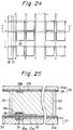
- Figs. 24 and 25 show an optical address type active-matrix driving type liquid crystal display device as disclosed in the Japanese Patent Application No.Hei5-100246 filed by the applicant of the present application.
- a basic substrate 21 composing a display panel includes a plurality of light waveguides Y1, Y2,.., Y n arranged vertically on a glass substrate 21a.
- a clad layer 23 is formed on the glass substrate 21a in a manner to cover these light waveguides Y1, Y2,.., Y n
- Signal wires X1, X2,...,X m are arranged horizontally in a manner to be crossed with the light waveguides Y1, Y2,.., Y n .
- a pixel electrode is formed in a manner to be substantially buried in each of the areas defined by the light waveguides Y1, Y2, . .
- Light switching elements 26, 26,.. each made of a photoconductive film are provided vertically between an extended portion of the pixel electrode 25 and the signal wires X1, X2,.., X m .
- a light cut-off layer 28a is provided inside of the glass substrate 21a in a manner to correspond to each of the light switching elements 26, 26,... This light cut-off layer 28a serves to prevent light (outer light) from the outer surface of the glass substrate 21a from being incident to the light switching element 26.
- an opposed electrode 29 made of a transparent conductive film.
- a light cut-off layer 28b is provided at the location corresponding to the light switching element 26 and serves to prevent light (outer light) from the outer surface of the opposed substrate 22 from being incident to the light switching element 26.
- an orientation film 27a or 27b is formed and is subject to an orientating treatment.
- the substrates 21 and 22 formed as described above are pasted with each other through a spacer 32 and a display medium 33 laid therebetween.
- this optical display type display device when a ray of light is applied from a luminous element array 30 to each light switching element 26 through a micro lens array 31, light waveguides Y1, Y2,..Y n , the light switching element 26 lowers its impedance so as to allow a signal voltage to be applied to the light switching element 26, thereby electrically connecting the signal wires X1, X2,.., X m with the pixel electrode 25.
- the light switching element 26 enhances its impedance. This results in electrically insulating the signal wires X1, X2, .. X m from the pixel electrode 25. That is, this optical address type display device is arranged to use a scan signal as a light signal and is driven by using the change of impedance of the light switching element 26.
- Figs. 26 and 27 show a positional relation among the light switching element 26, one light waveguide (for example, Y n ), one signal wire (for example, X m ) and a pixel electrode 25, on which the detailed explanation about it will be expanded.
- This display apparatus uses a method for picking up light from light scattering portions 24, 24.. by forming flaws which are located on the part of the light waveguide Y1, Y2,.. ,Y n corresponding to the light switching elements 26 for supplying a ray of light from the light waveguide Y1,Y2,..Y n to light switching elements 26,.. effectively.
- the part of the ray of light propagating through the light waveguides Y1, Y2, ..Y n are scattered at these light scattering portions and are emitted to the light switching elements 26 as a signal light.
- Fig. 28 shows a relation between quantity of light coming out of an end of the light waveguide and the number of the light scattering portions 24 on the light waveguide in the case that the light scattering portions 24 provided in all the light waveguides are the same with each other in size and form and a ray of light applies from the other end of the light waveguide.
- the quantity of light passed through the light waveguide and picked up out of the end of the light waveguide is attenuated exponentially as the light scattering portions are increased in number.
- the attenuation not proportional to the number but exponentially indicates that the quantity of picked light is different at each location. That is, the quantity of light picked up at each location is made smaller as the location goes further along the light waveguide from the light-incident side.
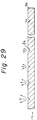
- Fig.29 shows a V groove of each light pick-up portion 24 and a light-applied state at the light pick-up portion 24 in the prior art.
- such a display device as impairing a light waveguide for forming a V groove as means for picking up light or such a display device as making the surface of the light waveguide coarse as disclosed in the Japanese Patent Lying Open No. Hei 1-224727 is required to mechanically or chemically work the light waveguide.
- the mechanical work may often impair a glass substrate.
- a high-level working technique is required.
- the working accuracy may be insufficient.
- a wet etching technique with a hydrogen fluoride etchant is used as the chemical work. In this case, the etching technique has difficulty in controlling the form and the size of the light pick-up portion.
- a method for impairing the light waveguide or making the surface coarse may be provided. This method makes it impossible to apply 100 % of the scattered light obtained from the light pick-up portion to the switching element, thereby making the light utilization efficiency worse.
- Fig. 16 is a plan view showing a structure of an optical address type active-matrix driving type LCD.
- Fig. 17 is a section cut on the A-A line of Fig. 16.
- a glass substrate 105b, a light cut-off layer 110, an orientation film 109b, a transparent electrode 106, a seal 107, a spacer 114 and a liquid crystal layer 108 are not shown though they are shown on the section shown in Fig. 17.
- a plurality of linear luminous sources Y1, Y2,.., Y n-1 , Y n are ranged in the Y direction.
- a plurality of linear electrodes X1, X2,.., X m-1 , X m are ranged in the X direction and in a manner to be crossed with the linear luminous sources, respectively.
- Each of the linear luminous sources Y1, Y2,.., Y n-1 , Y n is composed of an LED array element, a luminous portion 101 formed of an LD array element, a linear light waveguide 102 for transmitting a ray of light from the luminous portion 101, and a light pick-up portion 116 formed on the linear light waveguide 102.
- the luminous portion 101 By operating the luminous portion 101, the light is propagated through the linear light waveguide 102 and is applied to the upper part of the substrate through the effect of the light pick-up portion 116.
- a light switching element 103 made of a photoconductive layer.
- the linear electrodes X1, X2,.., X m-1 , X m are formed on the same level as the pixel electrode for driving a display medium, that is, liquid crystal.
- the light switching elements 103 are provided between the linear electrodes X1, X2,.., X m-1 , X m and the linear luminous sources Y1, Y2,.., Y n-1 , Y n , respectively.
- a transparent electrode 106 is formed on the other glass substrate 105b.
- the liquid crystal layer 108 is sealed between the substrate and the sealing member 107.
- the light switching element 103 When a ray of light is applied to the light switching element 103, that is, the linear luminous source Y2 is made operative, the light switching element 103 lowers its impedance so that a signal from the linear electrode X1 may be applied to the pixel electrode 104 for changing an orientating state of liquid crystal.
- an electric signal may be correspondingly applied to the linear electrodes X1, X2,..., X m-1 , X m .
- the linear luminous sources Y1, Y2,.., Y n-1 , Y n are made luminous, the light switching element on the linear luminous source is switched on.
- the electric signals from the linear electrodes X1, X2,.., X m-1 , X m may be applied to the pixel electrodes 104, respectively. That is, in place of an electric gate signal of a TFT film, the light signals from the linear luminous sources Y1, Y2,.., Y n-1 , Y n serve to scan the light switching element 103.
- a technique for forming a light waveguide and a method for picking up light are important to controlling light for switching the liquid crystal.
- As the technique for forming a light waveguide there has been proposed a method for melting an optical fiber on the light waveguide for forming a highly reliable and low-loss light waveguide (Sharp, Ltd.: Japanese Patent Application No. Hei4-4739)
- a method for scattering light with a flaw has difficulty in controlling quantity of picked light when working the element. Further, for forming a film with a high index of refraction, the clad layer has to be patterned. This is a disadvantage.
- a first object of the present invention is to improve a method for picking up light from a light waveguide to a light switching element and keep the quantity of picked light equal at all the pick-up location for realizing an even display characteristic over all the display.
- a second object of the present invention is to provide a display device which may be arranged to pick up light from a light waveguide without through the effect of mechanical work or chemical work, efficiently guide the light to the light switching element, keep the quantity of picked-up light equal at each location of picking up light, and realize an even display characteristic on the overall surface of the display.
- a third object of the present invention is to provide a large-capacitance and high-resolution optical scan type liquid crystal display element.
- the first object of the invention can be achieved by a display device comprising an insulated basic substrate, a plurality of light waveguides ranged on the basic substrate in parallel, a plurality of signal wires arranged in parallel and in a manner to be crossed with the light waveguides, respectively, a plurality of photoconductive layers three-dimensionally laid between the light waveguides and the signal wires at respective crosspoints between the light waveguides and the signal wires and for performing a switching operation in response to light sent from the light waveguides, a plurality of pixel electrodes provided in a manner to contact with the photoconductive layers and the light waveguides, an insulated opposed substrate located as opposed to the basic substrate with a display medium laid between the substrates and having an opposed electrode on the surface opposed to the basic substrate, light pick-up grooves provided at the corresponding locations to the photoconductive layers on the light waveguides and for guiding light transmitted through the light waveguides to the photoconductive layers, and the size of each of the grooves being increased progressively along a transmission path of each of
- the light pick-up groove may be V-formed.
- Some light pick-up grooves arranged along and adjacent to the light waveguide are assumed as one combination and the sizes of the light pick-up grooves are respective in the combinations of the grooves.
- the changing range of the light pick-up grooves is preferably 2 or more and 0.1n or less for n light pick-up grooves provided on one light waveguide.
- the second object of the invention can be achieved by a display device comprising an insulated basic substrate, a plurality of light waveguides ranged on the basic substrate and in parallel to each other, a plurality of signal wires arranged in parallel and in a manner to be crossed with the light waveguides, respectively, a plurality of photoconductive layers three-dimensionally laid between the light waveguides and the signal wires and directly connected with each light guiding portion of the light waveguides at respective crosspoints between the light waveguides and the signal electrodes and for performing a switching operation in response to a light signal from the light guiding portion, a plurality of pixel electrodes provided to be connected with the photoconductive layers, respectively, an insulated opposed substrate located in opposition to the basic substrate with a display medium therebetween and having an opposed electrode on the surface opposed to the basic substrate, and the relation among an index of refraction nl of the light guiding portion, an index of refraction n2 of the photoconductive layer, and an angle of incidence ⁇ of light given from the light guiding portion
- an area on the interface between the light guiding portion and the photoconductive layer is increased along a transmission path of the light waveguide.
- a middle layer may be provided at the interface between the light guiding portion and the photoconductive layer and the relation among an index of refraction n1 of the light waveguide, an index of refraction n2 of the photoconductive layer, an index of refraction n3 of the middle layer, and an angle of incidence ⁇ 1 of light given from the light guiding portion to the middle layer meets the following expression (2) of n1 sin ⁇ 1 ⁇ n2 and n1 sin ⁇ 1 ⁇ n3
- an area of the interface between the light guiding portion and the middle layer is increased progressively along a transmission path of the light guiding portion.
- the middle layer is made of a transparent conductive material.
- the display medium is made of liquid crystal.
- the third object of the invention can be achieved by a light pick-up portion having a high index of refraction formed on the clad layer formed on the top of the light waveguide through the effect of an ion exchange method.
- the light pick-up portion is located on the part of the light waveguide corresponding to the light switching portion.
- the method for exchanging ions is a method for forming a portion with a high index of refraction by replacing sodium ion (Na+) of soda glass with a monovalent metal ion.
- a monovalent metal ion is silver ion (Ag+) or thallium ion (Tl+).
- each form of the plural light pick-up grooves provided on the light waveguide is made larger along the transmission path so that the transmitted light may be strongly scattered. This compensates for attenuation of the quantity of picked-up light along the transmission path, thereby being able to keep the quantity of picked-up light at any light pick-up location on the light waveguide. This results in realizing an even light application on the light switching element at each location.
- the index of refraction defines the light waveguide and the photoconductive layer made of a material meeting the above-mentioned expression, the ray of light may be efficiently guided from the light waveguide to the photoconductive layer.
- the photoconductive layer lowers its impedance so as to enter an on state.
- a signal from the linear electrode is applied to the pixels of the liquid crystal layer through this photoconductive layer.
- the quantity of the picked light can be kept even at any place where the light pick-up portion is formed in the photoconductive layer on the light waveguide.
- each photoconductive layer serves to uniformly perform a switching operation at any place. This results in offering an even display characteristic over the screen.
- the form of this light pick-up portion makes the working easier.
- the size of this light pick-up portion may be changed at each of the light pick-up portions for easier working. If the total number n of the light pick-up portions is divided into 2 or more and 0.1n or less blocks and the size of the light pick-up portions may be changed at each block, both of the characteristics, that is, workability and light picking evenness may be satisfied.
- a light signal can be guided from the light waveguide to the photoconductive layer without mechanically working the light waveguide. Further, the contact area between the light waveguide and the photoconductive layer is made larger along the transmission path. The quantity of picked light is kept even at any place where the light pick-up portion is formed on the light waveguide. Hence, each photoconductive layer can evenly do a switching operation at any place. This results in offering a display device having an even display characteristic over the screen.
- a light signal can be guided from the light waveguide to the photoconductive layer side through the middle layer without mechanically working the light waveguide.
- provision of the middle layer makes it possible to more smoothly define the material for the light waveguide and the photoconductive layer.
- the contact area among the light waveguide, the middle layer and the photoconductive layer is made larger along the transmission path so that the quantity of the picked light is kept constant at any place where the light pick-up portion is formed on the light waveguide.
- the present invention is capable of patterning the light pick-up portion with high accuracy and suppressing the degrade resulting from the heating or cooling of the subsequent process. Hence, the light propagating characteristic of the light waveguide is guaranteed so that the light may be incident to the light switching portion with high accuracy and high efficiency. This results in making it possible to provide a high-capacitance and high-resolution liquid crystal display element.
- Fig. 1 is a plan view showing an optical address type active-matrix liquid crystal display device according to the embodiment 1 of the present invention.
- Fig. 2 is a view showing an element structure cut on the G-G' section.
- Fig. 3 is a sectional view showing a form of a light pickup portion on a light waveguide included in the embodiment 1 of the present invention.
- Fig. 4 is a sectional view showing an optical address type active-matrix liquid crystal display device according to the embodiment 2 of the present invention.
- Fig. 5 is a model view showing a light waveguide included in the display device according to the embodiment 3 of the present invention.
- Fig. 6 is a view showing a light pick-up intensity at each light pick-up portion.
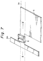
- Fig. 7 is a perspective view showing a positional relation among a signal wire, a light switching element and a pixel electrode in the embodiment 4 of the present invention.
- Fig. 8 is a sectional view cut on the B-B' line of Fig. 9 and Fig. 8 (a) shows a large window form of a clad layer and Fig. 8 (b) shows a small window form of the clad layer.
- Fig. 9 is a view showing a relation between an index of refraction n2 and an attenuating factor k against a ray of light with each wavelength, about amorphous silicon hydride (a-Si:H).
- Fig. 10 is a perspective view showing a positional relation among a signal wire, a light switching element and a pixel electrode in the embodiment 5 of the present invention.
- Fig. 11 is a sectional view cut on the A-A' of Fig. 9 and Fig. 119(a) shows a large window form of the clad layer and Fig. 11 (b) shows a small window form of the clad layer.
- Fig. 12 is a perspective view showing a positional relation among a signal wire, a light switching element and a pixel electrode in the embodiment 5 of the present invention.
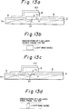
- Fig. 13 is a sectional view cut on the line C-C' of Fig. 12 and Fig. 13(a) shows a large window form of the clad layer and Fig. 13(b) shows a small window form of the clad layer.
- Fig. 14 is a view showing a light path formed when a ray of light passes through three layers having respective indexes of refraction.
- Fig. 15 is a plan view showing an optical address type simple-matrix liquid crystal display device according to the embodiment 6 of the present invention.
- Fig. 16 is a plan view showing an optical scan type active-matrix driving liquid crystal display device according to the present invention.
- Fig. 17 is a section cut on the A-A line of Fig. 16.
- Fig. 18 is a principle view showing a structure of a light waveguide and a method for picking up light shown in Fig. 17.
- Fig. 19 is a view showing a manufacturing process for a method for picking up light in an optical scan type LCD according to the present invention.
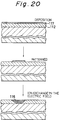
- Fig. 20 is a view showing a process for an ion exchanging method which is one kind of a method for picking up light in the optical scan type LCD according to the present invention.
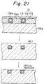
- Fig. 21 is a view showing another manufacturing process for a light waveguide included in the optical scan type LCD according to the present invention.
- Fig. 22 is a view showing another manufacturing process for a light waveguide included in the optical scan type LCD according to the present invention.
- Fig. 23 is a view showing another manufacturing process for a light waveguide included in the optical scan type LCD according to the present invention.
- Fig.24 is a view showing a conventional optical address type active-matrix liquid crystal display device filed by the applicant of the present application.
- Fig. 25 is a view showing an element structure cut on the H-H' line of Fig. 15.
- Fig. 26 is a perspective view showing a positional relation among a signal wire, a light switching element and a pixel electrode included in a conventional optical address type active-matrix liquid crystal display device filed by the applicant of the present application.
- Fig. 27 is a view showing an element structure cut on the D-D' line of Fig. 24.
- Fig. 28 is a view showing a relation between the quantity of light guided out of one end of the light waveguide when light is incident to the other end of the light waveguide and the number of light scattering portions on the light waveguide.
- Fig. 29 is a sectional view showing a form of a light pick-up portion on the light waveguide according to the prior art.
- Fig. 30 is a model view showing a light waveguide in the prior art.
- Figs. 1 and 2 show an arrangement of an optical address type active-matrix driving liquid crystal display device according to the present invention.
- a basic substrate 1 composing a liquid crystal panel is arranged to have a glass substrate la as a base and a plurality of light waveguides Y1, Y2,.., Y n arranged on the glass substrate la in the Y direction.
- the light waveguides Y1, Y2,.., Y n are formed by diffusing thallium ion (T1+) on the glass substrate la with heat and electric field and patterning the film.
- Each of the light waveguide Y1, Y2,.., Y n has one end connected to a luminous portion made of a luminous element array 10 and a micro lens array 11 common to these light waveguides.
- a high-output LD laser diode
- an LED Light-emitting Diode
- a clad layer 3 made of an SiO2 thin film is formed on the surface of the glass substrate 1a.
- a plurality of signal wires X1, X2,.., X m are located on the clad layer 3 in the X direction and in a manner to be crossed with the light waveguides Y1, Y2,.., Y n .
- These signal wires X1, X2,.., X m are made of Ti as a main material and are formed by the sputtering technique.
- a pixel electrode 5 made of a transparent conductive ITO film is provided on the clad layer 3. Part of the pixel electrode 5 is extended over each of the crossed portions between the light waveguides Y1, Y2,.., Y n and the signal wires X1, X2,.., X m .
- a light switching element 6 made of a photoconductive layer is provided between the extended part of the pixel electrode 5 and each of the signal wires X1, X2,.., X m at the location.
- the light switching element 6 is made of a photoconductive a-Si:H film.
- This a-Si:H film is formed to have a thickness of about 1 ⁇ m by means of a plasma CVD technique by using silane gas (SiH4) and Hydrogen (H2).
- SiH4 silane gas
- H2 Hydrogen
- a light cut-off layer 8a is provided inside of the glass substrate la. This light cut-off layer 8a serves to prevent light (outer light) from the outer surface of the glass substrate la from being incident to the light switching element 6.
- an opposed electrode 9 made of a transparent conductive ITO film is formed on the overall surface of the glass substrate 2a served as a basic material of the substrate 2.
- the light cut-off layer 8b is provided at the corresponding location to the light switching element 6 on this opposed electrode 9 and serves to prevent light (outer light) from the outer surface of the glass substrate 2a of the opposed substrate 2 from being incident to the light switching element 6.
- an orientation film 7a or 7b made of polyimide is coated by a spin-coating technique.
- the orientation film 7a or 7b is subject to the rubbing treatment.
- As the orientation film 7a or 7b it is possible to use an organic film such as a polyamide film, various LB films, an SiO film or an oblique evaporated film of SiO2. Both of the substrates 1 and 2 formed as above are pasted with a spacer 12 and a liquid crystal material 13 laid therebetween.
- the display device formed as above operates as follows.
- a light signal may be guided from the luminous element array 10 to the light waveguides Y1, Y2,.., Y n through a micro lens array 11.
- a light pick-up portion (light scattering portion) 4 is formed at each of the light switching elements 6.
- This light pick-up portion 4 is formed of a V groove on each of the light waveguides Y1, Y2,.., Y n by means of a blade, for example.
- a light signal propagated through the light waveguides Y1, Y2,.., Y n is scattered at the light pick-up portion 4 and then is applied to the light switching element formed at that location.
- the light switching element 6 changes its impedance according to a bright/dark state of the applied light so as to control flow of current to the signal wires X1, X2,.., X m and the pixel electrode 5 connected to the light switching element 6 for driving the liquid crystal 13. That is, in the light-applied state, the light switching element 6 lowers its impedance through the photoconductive effect so that the signal wires X1, X2,.., X m may be electrically conducted with the pixel electrode 5. This results in applying a data signal to the liquid crystal 13 between the pixel electrode 5 and the opposed electrode 9.
- the light switching element 6 raises its impedance so that the signal wires X1, X2,.., X m may be electrically insulated from the pixel electrode 5.
- no data signal is applied to the liquid crystal 13 between the pixel electrode 5 and the opposed electrode 9. Hence, the voltage applied to the liquid crystal 13 when light is applied is maintained.
- the V groove is made larger so that the area of the light scattering portion may be enlarged for compensating for the attenuated amount of the picked-up light. That is, as shown in Fig. 3, the V groove at the location near the light-incident side is shallow and small. The V groove is made gradually deeper and larger as it goes further from the light-incident side. With this design of the V groove, the quantity of light is kept equal in respective light pick-up portions 4, which makes it possible to provide all the light switching elements 5 with even element performance. This results in being able to obtain even display performance over all the screen of the display device.
- this optical address type liquid crystal display device uses a ray of light as a scan signal, unlike the electric signal, no delay of a signal waveform is brought about through the adverse effect of wire resistance and capacitance. Further, according to this embodiment, an even light signal can be sent to any location on the screen. This makes it possible to realize a high-definition display even in a large display device.
- the form of the light pick-up portion 4 is formed like a V groove.
- Another form like a U groove or a semi-spheric concave may be effectively used. Further, such forms are effective when light is picked up by using coarseness or grating on the surface.
- the present invention is effective if the light waveguides Y1, Y2,.., Y n are provided on the opposed substrate 2 and the light switching element 6 is mounted on a substrate and the light waveguides Y1, Y2,.., Y n are mounted on the other substrate in the optical address type active-matrix driving liquid crystal display device as disclosed in the Japanese Patent Application No. Hei 3-248110 filed by the applicant of the present application.
- Fig. 4 shows an arrangement of a liquid crystal display device according to the embodiment 2.
- the basic element arrangement of this embodiment is the same as the liquid crystal display device according to the embodiment 1, except that the light waveguides Y1, Y2,.., Y n for transmitting a light signal are provided on the inside of the opposed substrate 2 to the basic substrate 1 having the light switching element 6 formed thereon.
- a luminous element array and a micro lens array are not illustrated.
- the form of the light pick-up portion 4 is made larger as the light pick-up portion 4 goes further from the light-incident side along each light waveguide. This results in being able to obtain even display performance on the overall screen of the display device.
- the display device may take an arrangement that the light pick-up grooves have respective sizes for the light waveguides or an arrangement that a plurality of light pick-up grooves are assumed as one combination along the transmission path and the light pick-up grooves have respective sizes for the combinations.
- Fig. 5a is a model view showing a light waveguide provided in the display device according to this embodiment.
- the display device is arranged to divide the light pick-up portions into several blocks along the photoconductive transmission path. For each block, the size of the light pick-up groove is changed so that the reflective factor R viewed from the inside of the light waveguide may be changed.
- the other part of the arrangement is likewise to that of the display device according to the embodiment 1 or 2.
- a light signal entered from one end of the light waveguide as an incident ray at the light intensity I is picked out of the light waveguide at each light pick-up portion and then is applied to the light switching element provided near the light waveguide.
- the light pick-up portions (total number is n) are divided into M blocks each consisting of some portions. For each block, the light pick-up grooves have respective sizes so that the reflective factors of light viewed from the inside of the light waveguide are respective in the blocks.
- Fig. 6 shows the light pick-up intensity of each light pick-up portion in the conventional display device having a light waveguide as shown in Fig.
- each light pick-up portion provides a light pick-up groove having the same form and size so that the reflective factor R of light as viewed from the inside of the light waveguide may be kept constant.
- Each light pick-up portion serves to pick up light out of the light waveguide at a rate of (1-R) to the light reaching each light pick-up portion.
- a light of 10 mW may be picked out as compared to the incident ray of 14 mW.
- the conventional display device is arranged to pick up light of I(I-R) at the first light pick-up portion (1) and light of IR999(I-R) at the 1000th light pick-up portion (1000). It means that the first light pick-up portion (1) serves to pick up light of 0.0175 mW and the 1000th light pick-up portion (1000) serves to pick up light of 0.00502 mW. At each light pick-up portion (n), the light pick-up intensity is reduced exponentially with the increase of n and thus the light cannot be picked up at even light intensity.
- the light switching element is required to have such a conductive rate characteristic as sufficiently displaying an image even if the quantity of applied light is 0.00502 mW (corresponding to the 1000-th light pick-up portion).
- the light application is excessive if the quantity of the applied light is 0.0175 mW (corresponding to the first light pick-up portion). Hence, the performance of all the light switching element is not allowed to be kept even.
- the display device is arranged so that the intensity of light picked up at each light pick-up portion stays in the range of 0.01 ⁇ 0.002 mW.
- the substantially same intensity of light can be picked up on the overall area of the light waveguide.
- any light switching element may be used if it has such a conductive ratio characteristic as sufficiently displaying an image in the case of the quantity of the applied light of 0.008 mW. It may sufficiently correspond to the quantity of applied light of 0.012 mW. Hence, the performances of all the light switching elements are allowed to be kept even.
- the reflective factor R at each light pick-up portion may be defined as follows.
- the light reflective factor at the light pick-up portion viewed from the inside of the light waveguide may change into M kinds from R1 to R M .
- the light pick-up portion can be divided into M blocks, each of which includes n/M light pick-up portions.
- the light entered into the k-th block (reflective factor R k ) numbered along the transmission path of the light waveguide is attenuated by a factor of R n/M k .
- the light is incident to the block at the light intensity of I - (I - I' ) k/M and outgoes from the block at the intensity of I - (I - I') (k - 1)/M.
- the following expression (1) may be established among the reflective factor R k , the total number n of the light pick-up portions, the number M of divided blocks, the block number k, the light intensity I provided when light is incident to the light waveguide, and the light intensity I' provided when light outgoes from the light waveguide.
- R k can be defined at each block. With the value of R k , the size of the light pick-up groove can be set.
- the description has been expanded on the assumption that the number M of divided blocks (the kinds of size change) is 10.
- the number M of the divided blocks is set as 100, the quantity of light to be picked out of each light pick-up portion stays in the range of 0.01 ⁇ 0.0002 mW, which means that the picked light is made more even.
- the number M of divided blocks is set as a too many value, the kinds of the size changes of the light pick-up groove are made too many when working the device. As a result, the working is made difficult because the size is required to be finely controlled.
- the most approximate range of the number M of divided blocks is changed according to the number n of the light pick-up portions per one scan line (light waveguide). It is preferable to set the range as 2 or more but 0. ln or less.
- n light pick-up portions are divided into M blocks, the number of the divided blocks is n/M.
- Each block may include a different number of light pick-up portions.
- Figs. 7 and 8 show an arrangement of a liquid crystal display device according to the embodiment 4.
- the luminous element array and the micro lens array are not shown.
- an S i O2 film may be formed as a clad layer 3 by means of the sputtering technique.
- an a-Si:H film made of a photoconductive material is formed as a light switching element 6 by means of the plasma CVD technique and is patterned.
- the clad layer 3 is removed at the location where the light switching element 6 is formed. At this location, the light waveguides Y1, Y2,.., Y n come into direct contact with the light switching element 6.
- Parts of the signal wires X1, X2,..., X m are extended over to cover one end of the top of the light switching element 6.
- the other end of the top of the light switching element 6 is covered by the extended part of the pixel electrode 5 formed directly on the clad layer 3.
- Table 1 lists the index of refraction n1 of the general light waveguides Y1, Y2,.., Y n used in the optical address display device. Further, Fig. 9 shows a relation between an index of refraction n2 and an attenuating coefficient k of amorphous silicon hydride (a-Si:H) against the light having each wavelength (referred in "Amorphous Handbook" published by Science Forum, edition.).
- a-Si:H amorphous silicon hydride
- the ion (Tl+) diffused light waveguides are used as the light waveguides Y1, Y2,.., Y n .
- the index of refraction n1 of the light waveguide is about 1.67. Since the index of refraction n4 of the clad layer 3 is about 1.46, in the area where the clad layer 3 exists on the light waveguides Y1, Y2,.., Y n , only the light entered at an incident angle ⁇ 1 meeting the relation of; n1 sin ⁇ 1 >n4 is mirror-reflected on the interface so that the light may be propagated through the light waveguides Y1, Y2,..,Y n , where ⁇ 1 is an incident angle of a ray of light entered from the light waveguide to the clad layer 3.
- the clad layer 3 formed on the light waveguides Y1, Y2,.., Y n is removed so that the light waveguides Y1, Y2,.., Y n may directly contact with the light switching element 6.
- the index of refraction nl of the light waveguides Y1, Y2,.., Y n is about 1.67
- the relation among this index of refraction n1, the index of refraction n2 of the light switching element 6 and the incident angle ⁇ of the light formed between the light waveguides Y1, Y2,.., Y n and the light switching element 6 does not depend on the incident angle ⁇ .
- the relation of n1sin ⁇ n2 is constantly met.
- the direct contact between the light waveguides and the light switching element allows the light propagated inside of the light waveguides Y1, Y2,.., Y n to be entered to the light switching element 6 on the contact surface.
- the size of the removal pattern (window form) of the clad layer 3 in the light pick-up portion located on the further side from the luminous element shown in Fig. 8b is made larger than the size of the pick-up form of the light on the nearer side of the luminous element shown in Fig. 8d. Hence, at each spot, the even quality of light can be picked up. This makes it possible to provide all the light switching elements 6 with uniform performance.
- this embodiment does not bring about any problem such as breakage of a substrate or a light waveguide in the mechanical work, degrade of a working accuracy accompanied with abrasion of a blade used for the working, or a high cost. Further, it does not have any difficulty in finely controlling an impair or coarseness on the surface as in the case of the chemical working or in reproducibility.
- the light pick-up portion formed along one light waveguide may be divided into several blocks so that the size of the removal pattern of the clad layer 3 may be changed according to each block.
- Figs. 10 and 12 show a positional relation among the signal electrodes X1, X2,.., X m , the light switching element 6, the pixel electrode 5, and the light waveguides Y1, Y2,.., Y n according to the embodiment 5.
- Figs. 11a and 11c show an element structure as viewed from the sectional view of the A-A' line of Fig. 10.
- Figs. 13a and 13c show an element structure as viewed from the sectional view of the C-C' line of Fig. 11. Both of the element structures shown in Figs.
- the 10 and 12 are the essentially same for the purpose of picking up a light signal, except that both have respective forms of the connecting portions between the pixel electrode 5 and the signal electrodes X1, X2,.., X m connected to the switching element 6. That is, the clad layer 3 is removed at the place where the light switching element 6 is formed and part of the pixel electrode 5 intruded to the removed part of the clad layer 3 comes into contact with the light waveguides Y1, Y2,.., Y n . The light switching element 6 is formed in contact with this pixel electrode 5 so that the element 6 may be laid between the signal electrodes X1, X2,.., X m on the light switching element 6 and the pixel electrode 5.
- Fig. 14 shows a light path arranged so that a ray of light is entered at an incident angle ⁇ 1 from the layer L1 to the layer L3 and at an incident angle ⁇ 3 from the layer L3 to the layer L2, and outgoes at an incident angle ⁇ 3 to the layer L2.
- the condition that the light entered at the incident angle ⁇ 1 passes through the interface A is; n1sin ⁇ 1 ⁇ n3
- the condition that the light entered at the incident angle ⁇ 1 passes through the interface B is; n1sin ⁇ 1 ⁇ n2
- the light is allowed to be guided from the layer L1 to the layer L2.
- the addition of the middle layer L3 to the layers L1 and L2 makes it possible to more smoothly define the element structure.
- the embodiment 5 is arranged so that the pixel electrode 5 serves as the middle layer L3.
- the pixel electrode 5 is made of an ITO film and its index of refraction n3 is about 2.
- the index of refraction nl of the light waveguides Y1, Y2,.., Y n is 1.67.
- the relation of 1.67sin ⁇ 1 ⁇ 2 is established independently of the value of the incident angle q1 formed between the light waveguides Y1, Y2,.., Y n and the pixel electrode 5.
- the light signal propagated through the light waveguides Y1, Y2,.., Y n is allowed to be transmitted to the pixel electrode 5.
- the light switching element 6 formed on the pixel electrode 5 is made of a-Si:H, the index of refraction n2 of which is 4 to 5.
- n1sin ⁇ 1 ⁇ n2 can be established independently of the incident angle ⁇ 1 of light passed from the pixel electrode 5 to the light switching element 6.
- the light signal of the light waveguides Y1, Y2,.., Y n is allowed to be transmitted to the light switching element 6 through the pixel electrode 5.
- a material of the pixel electrode 5 as keeping the index of refraction n3 meeting the relations of n1sin ⁇ 1 ⁇ n3 and n1sin ⁇ 1 ⁇ n2, concretely, 1.67 or more index of refraction n3 in the condition that the index of refraction n2 is 4 to 5 irrespective of the incident angle ⁇ 1 of light passed from the pixel electrode 5 to the light switching element 6, In2O3 or SnO2 may be used in addition to the ITO film.
- the index of refraction n3 of the pixel electrode 5 has a small effect on the transmitted light.
- the condition for light transmittance is defined only by the index of refraction n1 of the light waveguides Y1, Y2,.., Y n and the index of refraction n2 of the light switching element 6. That is, if only the relation of n1sin ⁇ 1 ⁇ n2 is met, the light is allowed to be transmitted from the light waveguides Y1, Y2,.., Y n to the light switching element 6.
- the difference between the indexes of refraction or the method for picking up light may be used. It may offer the same effect as the embodiment 4.
- the size of a removal pattern (window form) of the clad layer 3 in the light pick-up portion on the further side from the luminous element shown in Fig. 11b or 13b is made larger than the size of the form for picking up light on the nearer side of the luminous element shown in Fig. 11d or 13d, for the purpose of picking up even quantity of light at any place. This makes it possible to provide all the light switching elements 6 with uniform performance.
- the area of the portion directly contacting the light guiding portions of the light waveguides Y1, Y2,.., Y n with the light switching element 6 or the area of the portion jointing the light guiding portions of the light waveguides Y1, Y2,.., Y n , the pixel electrode 5, and the light switching element 6 in the describing sequence, that is, the window form pattern of the clad layer 3 is allowed to be simply and accurately controlled by means of a photolithography technique. for example, the dry etching technique using CF4 gas or the wet etching technique using a hydrogen fluoride system etchant.
- a high-density display device for example, a high-definition display (HDTV) using about 1000 signal electrodes and about 1000 light switching elements 6 and the light pick-up portions per one of the light waveguides Y1, Y2, .., Y n , can be easily manufactured.
- HDTV high-definition display
- the light pick-up portions provided along one light waveguide are divided into several blocks so that the removal pattern of the clad layer 3 may be changed in size for each of the blocks.
- the optical address type display device may apply to the active-matrix driving type liquid crystal display device and a simple-matrix driving type liquid crystal display device proposed in the Japanese Patent Application No. Hei 3-258110 filed by the same applicant as the present application.
- Fig. 15 shows an arrangement of the liquid crystal display according to the embodiment 6.
- a plurality of light waveguides Y1, Y2,.., Y n are ranged in parallel in the Y direction.
- a plurality of signal wires X1, X2,.., X m are ranged in the X direction in a manner to be crossed with the light waveguides Y1, Y2,.., Y n .
- Pixel electrodes P 1,1 to P m,n are provided at the areas crossed between the adjacent light waveguides Y1, Y2,.., Y n and the signal wires X1, X2,.., X m , respectively.
- each of the light switching elements S 1.1 to S m.n is provided so that the corresponding one of the pixel electrodes P 1.1 to P m,n may be electrically connected with the corresponding one of the signal wires X1, X2,.., X m .
- the luminous element array and the micro lens array are not shown.
- the material may be selected to meet the relation referred in the embodiment 4 among the indexes of refractions of the light waveguides Y1, Y2,.., Y n , the pixel electrodes P 1,1 to P m,n , and the light switching elements S 1,1 to S m,n . This is for guiding the light signal to the light switching element so that the light switching element may operate.
- the liquid crystal display device described above operates as follows.
- the operation of the light switching elements S 1,1 to S m,n is the same as that of the light switching elements included in the active-matrix driving type liquid crystal display device indicated in the embodiment 1.
- the signal wires X1, X2,.., X m may be electrically conducted with or insulated from the pixel electrodes P 1,1 to P m,n according to the bright/dark of the light-applied state for performing a switching operation.
- a light scan signal is transmitted to the light waveguides Y1, Y2,.., Y n in sequence so that the signal wires X1, X2,.., X m may be electrically conducted with the pixel electrodes P 1.1 to P m,n in sequence.
- a simple multiplexing drive can be done between the pixel electrodes P 1,1 to P m,n and the combination of each three transparent electrode wires opposed to the corresponding pixel electrode. That is, the display area composed of each three striped transparent electrodes (scan electrode) is assumed as one unit block and each block is selected by the light waveguides Y1, Y2,.., Y n . As a result, as keeping a duty ratio constant, the number of the scan lines is allowed to be tripled. In general, assuming that the number of the light waveguides is N and the number of transparent electrodes (scan line) per one light waveguide is M, N x M scan lines can be driven at a duty ratio of 1/M.
- amorphous silicon germanium hydride (a-SiGe x :H) may be used against a ray of light having a near red infrared wavelength.
- the thin film of a-SiGe x :H may be formed by means of the plasma CVD technique using SiH4 gas and GeH4 gas.
- the LD or LED arranged to apply a ray of light having a near infrared wavelength (800 nm to 1000 nm band) has been developed for optical communication and thus is relatively inexpensive.
- the high-output LD or LED has been also developed. In the cause of using these light sources for applying a light scan signal, it is desirous to compose the light switching element made of a-SiGe x :H having a high sensitivity against a ray of light having a near infrared wavelength.
- the light switching element may take a diode structure (for example, pin type, a Schottky type or MIS (Metal-Insulator-Semiconductor) type) of a photoconductive semiconductor, a back-to-back structure having two diodes series-connected in reverse or a diode ring structure having two diodes parallel-connected in reverse.
- a diode structure for example, pin type, a Schottky type or MIS (Metal-Insulator-Semiconductor) type
- any type of waveguide may be used if it meets the condition about light guiding performance and manufacturing process, such as ion-diffused glass waveguide, a quartz system waveguide formed by the flame deposition technique or the CVD technique, a waveguide made of a polymer material, a quartz fiber, or a plastic fiber. If the fiber is used, in place of the clad layer indicated in this embodiment, the clad provided in the fiber itself may be used.
- the liquid crystal display device uses a TN (Twisted Nematic) mode and is made of a fluorine system liquid crystal ZLI4792 manufactured by the MERCK company.
- a liquid crystal display mode for the nematic liquid crystal a guest host mode, a STN (Super Twisted Nematic) mode or a phase transition mode may be used.
- SSFLC Surface Stabilized Ferroelectric Liquid Crystal
- PDLC Polymer Dispersed Liquid Crystal
- the structure of the transmission type liquid crystal display device belonging to the optical address type liquid crystal display device may be effective as a reflective type liquid crystal display device if a reflective material may be use for a pixel electrode or a metal film. Further, a color filter is added inside of a panel for implementing the color display.
- liquid crystal display device Liquid Crystal Display
- LCD Liquid Crystal Display
- ECD electrochromic Display
- EPD Electrophoretic Display Device
- Fig. 16 is a plan view showing a basic structure of an optical address type driving LCD according to an embodiment of the present invention.
- Fig. 17 is a section showing a basic structure of an optical address type driving LCD according to the first embodiment of the present invention.
- Fig. 17 is a section cut on the A-A line of Fig. 16.
- Fig. 18 shows the detailed structure and principle of a light waveguide shown in Fig. 17.
- Fig. 19 shows a process for manufacturing a light waveguide.
- Fig. 20 is a process for creating a light pick-up portion through the effect of an ion exchange method.
- a glass substrate 105b, a transparent electrode 106, a liquid crystal layer 108, a spacer 114 and a seal 107 are not shown though they are shown on the section of Fig. 17.
- a plurality of linear luminous sources Y1, Y2,.., Y n-1 , Y n are ranged in the Y direction from Y1 to Y n .
- a plurality of linear electrodes X1, X2,..., X m-1 , X m are ranged in the X direction and in a manner to be crossed with the linear luminous sources, respectively.
- each of the linear luminous sources Y1, Y2,..., Y n-1 , Y n for example, the linear luminous source Y2 is composed of an LED array element, a luminous portion 101 formed of an LD array element, a linear light waveguide 102 for transmitting a ray of light from the luminous portion 101, and a light pick-up portion 116 formed on the linear light waveguide 102.
- the luminous portion 101 By operating the luminous portion 101, the light is propagated to the linear luminous source Y2.
- a light pick-up portion 116 is formed by giving a high index of refraction to the clad layer.
- the light propagated through the linear luminous source Y2 is guided to the photoconductive layer 103.
- the light switching element 103 made of a photoconductive layer is provided adjacent to each of the crosspoints between the linear luminous sources Y1, Y2,.., Y n- 1 Y n and the electrodes X1, X2,.., X m-1 , X m .
- the electrodes X1, X2,.., X m-1 , X m are formed on the same plane as the pixel electrode 104 for driving a display medium, that is, liquid crystal.
- the transparent electrode 106 is formed on the other glass substrate 105b.
- the liquid crystal layer 108 is sealed between the glass substrate and a sealing agent 107.
- the light switching element 103 When a ray of light is applied to the light switching element 103, that is, the linear luminous source Y2 is made operative, the light switching element 103 lowers its impedance so that the signal from the linear electrode X1 may be applied to the pixel electrode 104, thereby changing an orientating state of liquid crystal.
- the glass substrates 105a, 105b are one embodiment of two substrates of the present invention.
- the light switching element 103 is an embodiment of a photoconductive layer of the present invention.
- the liquid crystal layer is an embodiment of a liquid crystal layer of the present invention.
- the linear luminous sources Y1, Y2,.., Y n-1 , Y n are an embodiment of linear luminous sources of the present invention.
- the linear electrodes X1, X2,.., X m-1 , X m are one embodiment of linear electrodes of the present invention.
- the electric signal may be correspondingly applied to the linear electrodes X1, X2,..., X m-1 , X m .
- the picked ray of light guided from the linear luminous sources Y1, Y2,.., Y n-1 , Y n serves to put the light switching element to an on state.
- the electric signals from the linear electrodes X1, X2,.., X m-1 , X m are applied to the corresponding pixel electrodes 104. That is, in place of the TFT element electric gate signal, the light signals from the linear luminous sources Y1, Y2,.., Y n-1 , Y n are used for scanning the light switching elements 103.
- the scan signal is light
- no unfavorable state takes place where a scan (gate) signal is flown through the electric capacitance of the element like the TFT element.
- the rays of light from the linear luminous sources Y1, Y2,.., Y n-1 , Y n are allowed to be efficiently guided to the light switching portion according to the distribution of indexes of refraction.
- the light waveguide 102 is formed as shown in Fig. 19 and the light pick-up portion 116 is formed as shown in Fig. 20.
- a glass fiber Z (composed of a light cut-off layer 111, a clad 112, and a core 113) having a light cut-off layer 111 coated thereon and a glass plate 105c made of the same material as the glass substrate 105a are ranged alternately and then are molten with a glass plate 105d.
- the glass 105d is abraded for removal.
- the light cut-off layer 111 of the fiber on the substrate and part of the clad 112 are removed by abrasion.
- the amount is variable according to the index of refractions of the core and the clad. For example, 1 ⁇ m or more).
- ions are diffused on the fiber surface in a manner to match to the light switching portions for giving a high index of refraction to the part of the fiber surface. This part of the fiber surface serves as the light pick-up portion 116 for guiding the light being propagated through the core to the photoconductive layer 103.
- silver (Ag) 117 is formed as a thickness of 10 nm to 500 nm, preferably, 100 nm to 200 nm by the sputtering technique.
- the silver film is patterned according to the light switching portions.
- the silver ion (Ag+) is exchanged with sodium ion (Na+) in the fiber under the voltage of 50 V.
- the film is heated to thermally diffuse the ions.
- an Ag film having a thickness of 20 nm is evaporated and an ion exchanging portion 116 having a thickness of 10 ⁇ m is formed for about 20 minutes at the voltage of an electric field of 30 V/mm and at the temperature of 220°C.
- the thermal diffusion of Ag+ is executed for two hours and at 370°C. These processes result in forming a portion with a high index of refraction having a thickness of about 30 ⁇ m.
- Tl+ may be used as ions to be exchanged.
- molten salts such as AgNO3 (melting point 208° C) and TINO3 (melting point 230° C) may be used.
- a kind of metal such as titanium (Ti) may be patterned in advance so as to use it as a mask and the ion exchange in the electric field may be carried out in each molten salt.
- the diameter of the fiber may be set as 20 to 500 ⁇ m, preferably, 50 to 100 ⁇ m in a manner to match to the size of the photoconductor.
- the width of the glass 105c may be set as 50 to 500 ⁇ m, preferably, 200 to 300 ⁇ m in a manner to match to the size of a pixel.
- This photoconductive layer 103 is formed by forming an amorphous silicon hydride (a-Si:H) film by means of a plasma chemical vapor deposition (P-CVD) technique and patterning the film by means of an etching technique.
- a-Si:H amorphous silicon hydride
- P-CVD plasma chemical vapor deposition
- a-SiGe:H amorphous silicon germanium hydride
- a-SiC:H amorphous silicon carbide hydride
- a-SiO:H amorphous silicon oxide hydride
- a-SiN:H amorphous silicon nitride hydride
- the linear electrodes X1, X2,.., X m-1 , X m are formed by forming metal such as Al by means of the EB deposition technique and patterning the metal by the etching technique.
- metal such as Mo, Cr and Ti or a transparent electrode made of indium-tin oxide (ITO).
- the pixel electrode 104 is formed by depositing the ITO film by means of the sputtering technique and patterning it by means of the etching technique.
- the linear electrode X and the pixel electrode 104 are formed on the photoconductive layer 103.
- the photoconductive layer 103 may be formed on the linear electrode X and the pixel electrode 104.
- the structure composed of the linear electrode X, the photoconductive layer 103, and the pixel electrode 104 takes a planar type but it may take a sandwiched type.
- an orientation layer 109a is formed.
- the orientation layer 109a may be formed by forming a polyimide film by a spinner and rubbing the polyimide film. In place of the spinner, a printing method may be used for forming the orientation layer 109a.
- a transparent electrode 106 may be formed on the other glass substrate 105b.
- This transparent electrode 106 may be formed by depositing ITO by means of the sputtering technique.
- a light cut-off layer 110 is formed in a manner to match to the patterns of the light switching element composed of the photoconductive layer 103 formed on the opposed substrate.
- This light cut-off layer 110 is formed of Al with the EV deposition technique and etching the Al film.
- a metal such as Mo, Cr, or Ti, an organic pigment dispersed resin and an inorganic pigment dispersed resin may be used.
- the layer 110 is formed on the transparent electrode 106 herein, it may be formed on the rear side of the glass substrate 105b.
- orientation layer 109b is formed on these layers.
- This orientation layer 109b is formed by rubbing the polyimide film formed by a spinner. Though the orientation layer 109b is formed with a spinner, the printing method may be used for forming it.
- a spacer 114 (not shown) is dispersed. Then, both of the substrates are pasted with each other with a sealing agent 107.
- the liquid crystal layer 108 is formed by injecting liquid crystal between the substrates.
- the thickness of the liquid crystal layer 108 is about 5 ⁇ m.
- the display mode is a twisted nematic normally white type.
- the liquid crystal layer 108 is formed by injecting in vacuum PCH liquid crystal ZLI-1565 manufactured by the MELK company.
- the light switching element 103 When a ray of light is applied to the light switching element 103, that is, the linear luminous source Y2 is made operative, the light switching element 103 lowers its impedance so that the signal from the linear electrode X1 may be applied to the pixel electrode 104, thereby changing the orientating state of the liquid crystal.
- Fig. 21 shows a method for producing a light waveguide according to another embodiment of the invention.
- a glass fiber Z1 (composed of a clad 112 and a core 113) and a glass plate 105c made of the same material as the glass substrate 105a are alternately ranged on the glass substrate 105a.
- a preform of a glass paste (manufactured by Nippon Electric Glass, Ltd) is laid between the glass fiber Z1 and the glass substrate 105a so that a glass 105d may be put on and molten with them.
- the glass paste 115 is produced according to the characteristics (thermal expansion coefficient, glass transition point, and the like) of the glass substrate 105a, the glass plate 105c and the glass fiber Z1.
- the glass transition point of the glass paste 115 is somewhat lowered than the glass substrate 105a, the glass plate 105c and the glass fiber Z1. Since the glass paste 115 is black, it may serve as the light cut-off layer.
- the glass 105d is abraded to make the fiber portion appear on the surface. Further, part of the clad 112 of the fiber on the surface of the substrate is abraded for removal. At this time, it is necessary to leave such an amount of the clad on the surface of the substrate as inhibiting to leak the light being propagated inside of the light waveguide. (The amount is variable according to the indexes of refraction of the core and the clad, for example, 1 ⁇ m or more).
- ions are diffused on the surface of the fiber in a manner to match to the light switching portion so as to give the fiber surface a high index of refraction.
- the light pick-up portion 116 is formed for guiding the light being propagated in the core to the photoconductive layer 103.
- a silver (Ag) film is formed on the fiber surface in a manner to have a thickness of 10 nm to 500 nm, preferably, 100 nm to 200 nm and the film is patterned according to the light switching portions.
- sodium ions (Na+) in the fiber are exchanged with the silver ions (Ag+). If Ag+ is further diffused, the film is heated for thermally diffusing Ag+ ions.
- the Ag+ film of 200 nm is deposited and the ion exchange portion having the thickness of 10 ⁇ m is formed for about 20 minutes and at the temperature of 220° C and the electric field of 30 V/mm. Further, by thermally diffusing Ag+ ions at the temperature of 370° C and for two hours, it is possible to form a portion with a high index of refraction having a thickness of about 30 ⁇ m.
- the Ag+ ions to be exchanged with the sodium ions may be replaced with Tl+ ions.
- the dry ion exchange method for depositing the Ag film is used. In place, molten salts such as AgNO3 (melting point 208 °C) and TlNO3 (melting point 230 °C) may be used.
- the patterned metal film of titanium (Ti) is prepared for a mask.
- the ions are exchanged in the electric field in each molten salt.
- the intensity of the electric field, the time and the temperature may be adjusted according to the desired thickness of diffusion.
- the diameter of the fiber Z1 may be set as 20 to 500 ⁇ m, preferably, 50 to 100 ⁇ m in a manner to match to the size of the photoconductor.
- the width of the glass paste 15 is according to the diameter of the fiber.
- the width of the glass 5c may be set as 50 to 500 ⁇ m, preferably, 200 to 300 ⁇ m according to the size of each pixel.
- Fig. 22 shows a method for producing a light waveguide according to another embodiment of the present invention.
- a patterned resist is formed on the glass substrate 105a.
- a groove is formed by means of a sand-blast technique.
- a glass fiber Z (composed of a light cut-off layer 111, a clad 112 and a core 113) is fitted and molten in the groove.
- the sectional form of the groove is rectangular. In actual, it may be semicircular or V-formed.
- a blade may be used in place of the sand-blast technique.
- an etching technique may be used. Both of the mechanical working and the chemical working may be effective.
- the mechanical working is performed and then the chemical working is performed.
- a glass plate d may be put on the glass fiber and molten with it.
- the glass 105d is required to be removed by the abrasion after melting.
- the parts of the light cut-off layer 111 and the clad 112 of the fiber on the substrate surface are abraded for removal. It is necessary to lead such an amount of clad on the substrate surface as inhibiting to leak the light being propagated inside of the light waveguide. (The amount is variable according to the indexes of refraction of the core and the clad, for example, 1 ⁇ m or more).
- ions are diffused on the fiber surface in a manner to match to the light switching portions for enhancing the indexes of refractions of the parts so that the light pick-up portion 116 may be formed for guiding the light being propagated in the core to the photoconductive layer 3.
- the silver (Ag) is formed on the fiber surface by means of the sputtering technique in a manner to have a thickness of 10 nm to 500 nm, preferably, 100 nm to 200 nm by the sputtering technique.
- the film is patterned according to the light switching portions. Then, the silver ions (Ag+) are exchanged with sodium ions (Na+) in the fiber under the voltage of 50 V.
- the film is heated for thermally diffusing the Ag+ ions.
- an Ag film having a thickness of 200 nm is deposited.
- a portion with a high index of refraction can be formed to have a thickness of about 30 ⁇ m.
- the ions to be exchanged with the sodium ions the ions of Ag+ are used in this embodiment.
- Tl+ ions may be used.
- the dry ion exchange technique is used for depositing the Ag film.
- molten salts such as AgNO3 (melting point 208° C) and TlNO3 (melting point 230° C) are used.
- the patterned metal film of titanium (Ti) is prepared as a mask. With the mask, the electric field ion exchange may be carried out in each molten salt. The intensity of an electric field, the time and the temperature may be adjusted to match to a desired thickness of diffusion.
- the diameter of the fiber Z may be set as 20 to 500 ⁇ m, preferably, 50 to 100 ⁇ m in a manner to suit to the size of the photoconductor.
- the width of the glass 105c may be set as 50 to 500 ⁇ m, preferably, 20 to 300 ⁇ m in a manner to suit to the size of each pixel.
- Fig. 23 shows a method for producing a light waveguide according to another embodiment.
- a groove is formed by means of the sand-blast technique.
- a preform 115 of the glass paste for example, manufactured by the NEC Glass, Ltd
- the glass fiber composed of the clad 112 and the core 113 are fitted to the groove in the describing sequence and are molten.
- the used glass paste 115 is produced according to the characteristics of the glass substrate 105a, the glass plate 105c and the glass fiber Z1 (thermal expandability, glass transition point, etc.).
- the glass transition point of the glass paste 115 is somewhat made lower than those of the glass substrate 105a, the glass plate 105c and the glass fiber Z1. Since the glass paste 115 is black, it serves as a light cut-off layer.
- the section of the groove is rectangular. In actual, however, it may be semicircular or V-formed.
- a blade may be used in place of the sand-blast technique indicated in the embodiment.
- the etching technique may be used. Both of the mechanical working and the chemical working may be effective. Preferably, the mechanical working and then the chemical working may be done in this order.
- a glass plate 105d may be put before melting. The glass 105d is removed by abrasion after melting. Part of the clad 112 of the fiber on the substrate surface is removed by abrasion.
- Such an amount of the clad on the substrate surface as inhibiting to leak light being propagated inside of the light waveguide has to be left.
- the amount is variable according to the indexes of refraction of the core and the clad.
- ions are diffused on the fiber surface in a manner to suit to the light switching portions so as to enhance the index of refraction of the fiber surface for forming the light pick-up portion 116 for guiding the light being propagated in the cores to the photoconductive layer 103.
- Silver (Ag) is formed on the fiber surface to have a thickness of 10 nm to 500 nm, preferably, 100 nm to 200 nm by means of the sputtering technique. The silver film is patterned according to the light switching portions.
- the silver ions (Ag+) are exchanged with sodium ions (Na+) in the fiber at the voltage of 50 V.
- the film is heated for thermally diffusing the Ag+ ions.
- an Ag film having a thickness of 200 nm is deposited.
- the ion exchanging portion having a thickness of 10 ⁇ m is allowed to be formed at the temperature of 220° C and an electric field of 30 V/mm and for about 20 minutes.
- a portion with a high index of refraction having a thickness of about 30 ⁇ m can be formed.
- the ions to be exchanged are Ag+ ions.
- Tl+ ions may be used.
- the dry ion exchange method is used for depositing an Ag film.
- molten salts such as AgNO3 (melting point 208° C) and TlNO3 (melting point 230° C) may be used and the titanium metal patterned film is used as a mask. With the mask, the electric field ion exchange may be executed in each molten salt.
- the intensity of an electric field, the time and the temperature may be adjusted in a manner to suit to a desired diffusing thickness.
- the diameter of the fiber may be set as 20 to 500 ⁇ m, preferably, 50 to 100 ⁇ m in a manner to suit to the size of the photoconductor.
- the width of the glass paste is set according to the diameter of the fiber.
- the width of the glass 105c may be set as 50 to 500 ⁇ m, preferably, 200 to 300 ⁇ m in a manner to suit to the size of the pixel.
Landscapes
- Physics & Mathematics (AREA)
- Nonlinear Science (AREA)
- Mathematical Physics (AREA)
- Chemical & Material Sciences (AREA)
- Crystallography & Structural Chemistry (AREA)
- General Physics & Mathematics (AREA)
- Optics & Photonics (AREA)
- Liquid Crystal (AREA)
Applications Claiming Priority (9)
| Application Number | Priority Date | Filing Date | Title |
|---|---|---|---|
| JP29180692 | 1992-10-29 | ||
| JP29180692 | 1992-10-29 | ||
| JP291806/92 | 1992-10-29 | ||
| JP1292993A JPH06194682A (ja) | 1992-10-29 | 1993-01-28 | 光アドレス型表示装置 |
| JP12929/93 | 1993-01-28 | ||
| JP1292993 | 1993-01-28 | ||
| JP8461193A JP2944013B2 (ja) | 1993-04-12 | 1993-04-12 | 光走査型液晶表示素子及びその製造方法 |
| JP8461193 | 1993-04-12 | ||
| JP84611/93 | 1993-04-12 |
Publications (3)
| Publication Number | Publication Date |
|---|---|
| EP0595647A2 true EP0595647A2 (de) | 1994-05-04 |
| EP0595647A3 EP0595647A3 (de) | 1995-03-22 |
| EP0595647B1 EP0595647B1 (de) | 2002-12-18 |
Family
ID=27280048
Family Applications (1)
| Application Number | Title | Priority Date | Filing Date |
|---|---|---|---|
| EP93308654A Expired - Lifetime EP0595647B1 (de) | 1992-10-29 | 1993-10-29 | Optisch adressierte Anzeigevorrichtung |
Country Status (3)
| Country | Link |
|---|---|
| US (1) | US5528399A (de) |
| EP (1) | EP0595647B1 (de) |
| DE (1) | DE69332579T2 (de) |
Cited By (1)
| Publication number | Priority date | Publication date | Assignee | Title |
|---|---|---|---|---|
| EP1569280A3 (de) * | 1998-09-04 | 2006-06-07 | Seiko Epson Corporation | Bauelement mit Mitteln zur Lichtübertragung |
Families Citing this family (29)
| Publication number | Priority date | Publication date | Assignee | Title |
|---|---|---|---|---|
| FR2709567B1 (fr) * | 1993-09-03 | 1995-09-29 | Commissariat Energie Atomique | Dispositif de visualisation à conversion de faisceau laser en lumière visible et incohérente. |
| US5544268A (en) * | 1994-09-09 | 1996-08-06 | Deacon Research | Display panel with electrically-controlled waveguide-routing |
| US7167155B1 (en) | 1995-07-20 | 2007-01-23 | E Ink Corporation | Color electrophoretic displays |
| US7071913B2 (en) | 1995-07-20 | 2006-07-04 | E Ink Corporation | Retroreflective electrophoretic displays and materials for making the same |
| US7106296B1 (en) | 1995-07-20 | 2006-09-12 | E Ink Corporation | Electronic book with multiple page displays |
| US6067185A (en) | 1997-08-28 | 2000-05-23 | E Ink Corporation | Process for creating an encapsulated electrophoretic display |
| US7242513B2 (en) | 1997-08-28 | 2007-07-10 | E Ink Corporation | Encapsulated electrophoretic displays having a monolayer of capsules and materials and methods for making the same |
| US6839158B2 (en) | 1997-08-28 | 2005-01-04 | E Ink Corporation | Encapsulated electrophoretic displays having a monolayer of capsules and materials and methods for making the same |
| NO306588B1 (no) * | 1998-01-15 | 1999-11-22 | Kjell Hansen | Skjerm for bildefremvisning og/eller -opptak |
| US6704133B2 (en) | 1998-03-18 | 2004-03-09 | E-Ink Corporation | Electro-optic display overlays and systems for addressing such displays |
| US7075502B1 (en) | 1998-04-10 | 2006-07-11 | E Ink Corporation | Full color reflective display with multichromatic sub-pixels |
| US6473072B1 (en) | 1998-05-12 | 2002-10-29 | E Ink Corporation | Microencapsulated electrophoretic electrostatically-addressed media for drawing device applications |
| US7256766B2 (en) * | 1998-08-27 | 2007-08-14 | E Ink Corporation | Electrophoretic display comprising optical biasing element |
| WO2000020921A1 (en) | 1998-10-07 | 2000-04-13 | E Ink Corporation | Capsules for electrophoretic displays and methods for making the same |
| US7038655B2 (en) | 1999-05-03 | 2006-05-02 | E Ink Corporation | Electrophoretic ink composed of particles with field dependent mobilities |
| US6693620B1 (en) | 1999-05-03 | 2004-02-17 | E Ink Corporation | Threshold addressing of electrophoretic displays |
| US8115729B2 (en) | 1999-05-03 | 2012-02-14 | E Ink Corporation | Electrophoretic display element with filler particles |
| US6754408B2 (en) * | 2000-10-23 | 2004-06-22 | Sony Corporation | Optical switch and display unit |
| US7202847B2 (en) | 2002-06-28 | 2007-04-10 | E Ink Corporation | Voltage modulated driver circuits for electro-optic displays |
| AU2002354445A1 (en) * | 2001-12-07 | 2003-06-17 | Sharp Kabushiki Kaisha | Display apparatus using bidirectional two-terminal element and display apparatus manufacturing method |
| AU2002357842A1 (en) | 2001-12-13 | 2003-06-23 | E Ink Corporation | Electrophoretic electronic displays with films having a low index of refraction |
| US6754417B2 (en) * | 2002-04-24 | 2004-06-22 | Agilent Technologies, Inc. | Optical fiber tap capable of random placement along an optical fiber |
| JP2004062152A (ja) * | 2002-06-03 | 2004-02-26 | Sharp Corp | 双方向二端子素子を用いた表示装置およびその製造方法 |
| US7312916B2 (en) | 2002-08-07 | 2007-12-25 | E Ink Corporation | Electrophoretic media containing specularly reflective particles |
| GB2418717B (en) * | 2004-09-29 | 2009-08-12 | Miniflex Ltd | Linear member |
| US7251401B2 (en) * | 2005-09-16 | 2007-07-31 | Matshsita Electric Industrial Co., Ltd. | Fiber coating processing and slitting for non-confined light leakage |
| TWI424394B (zh) * | 2009-11-27 | 2014-01-21 | Chunghwa Picture Tubes Ltd | 一種顯示裝置與測量其表面結構的方法 |
| WO2011125102A1 (ja) * | 2010-04-02 | 2011-10-13 | 株式会社 東芝 | 表示装置 |
| JP2022527696A (ja) | 2019-03-29 | 2022-06-03 | イー インク コーポレイション | 電気光学ディスプレイおよびそれを駆動する方法 |
Family Cites Families (16)
| Publication number | Priority date | Publication date | Assignee | Title |
|---|---|---|---|---|
| US3838908A (en) * | 1973-02-22 | 1974-10-01 | Rca Corp | Guided light structures employing liquid crystal |
| JPS5643609A (en) * | 1979-09-19 | 1981-04-22 | Nippon Telegr & Teleph Corp <Ntt> | Optical fiber branching device |
| NO159899C (no) * | 1986-03-25 | 1989-02-15 | Kjell Hansen | Skjerm for bildefremvisning og/eller -opptak. |
| EP0278038A1 (de) * | 1987-02-13 | 1988-08-17 | Battelle-Institut e.V. | Aktiver Bildschirm in Flachbauweise |
| JPS63253903A (ja) * | 1987-04-10 | 1988-10-20 | Mitsubishi Rayon Co Ltd | 光フアイバ照光装置 |
| US4952031A (en) * | 1987-06-19 | 1990-08-28 | Victor Company Of Japan, Ltd. | Liquid crystal display device |
| JPH01173016A (ja) * | 1987-12-28 | 1989-07-07 | Toray Ind Inc | 光導電体を用いた液晶表示装置 |
| JP2518345B2 (ja) * | 1988-03-04 | 1996-07-24 | カシオ計算機株式会社 | アクティブマトリクスパネル |
| JPH0797190B2 (ja) * | 1988-09-26 | 1995-10-18 | 松下電器産業株式会社 | 記憶装置および液晶表示装置 |
| JPH02134617A (ja) * | 1988-11-15 | 1990-05-23 | Seiko Epson Corp | 電気光学装置 |
| US5009483A (en) * | 1989-04-12 | 1991-04-23 | Rockwell Iii Marshall A | Optical waveguide display system |
| CA2055123C (en) * | 1990-11-09 | 1996-06-11 | Naofumi Kimura | Display apparatus |
| DE4114629A1 (de) * | 1991-04-30 | 1992-11-05 | Siemens Ag | Lichtwellenleiter mit einer koppelflaeche |
| JP3005322B2 (ja) * | 1991-07-05 | 2000-01-31 | 三洋電機株式会社 | 液晶表示装置 |
| US5307186A (en) * | 1991-08-09 | 1994-04-26 | Sharp Kabushiki Kaisha | Liquid crystal light valve having capability of providing high-contrast image |
| US5170448A (en) * | 1992-01-06 | 1992-12-08 | Motorola, Inc. | Optical waveguide apparatus and method for partially collecting light |
-
1993
- 1993-10-29 US US08/146,487 patent/US5528399A/en not_active Expired - Lifetime
- 1993-10-29 EP EP93308654A patent/EP0595647B1/de not_active Expired - Lifetime
- 1993-10-29 DE DE69332579T patent/DE69332579T2/de not_active Expired - Fee Related
Cited By (1)
| Publication number | Priority date | Publication date | Assignee | Title |
|---|---|---|---|---|
| EP1569280A3 (de) * | 1998-09-04 | 2006-06-07 | Seiko Epson Corporation | Bauelement mit Mitteln zur Lichtübertragung |
Also Published As
| Publication number | Publication date |
|---|---|
| EP0595647B1 (de) | 2002-12-18 |
| DE69332579D1 (de) | 2003-01-30 |
| EP0595647A3 (de) | 1995-03-22 |
| US5528399A (en) | 1996-06-18 |
| DE69332579T2 (de) | 2003-07-31 |
Similar Documents
| Publication | Publication Date | Title |
|---|---|---|
| EP0595647B1 (de) | Optisch adressierte Anzeigevorrichtung | |
| US5589961A (en) | Optical wave guide driven liquid crystal display employing optical switching for input | |
| EP0490484B1 (de) | Anzeigevorrichtung | |
| KR100295300B1 (ko) | 레티노이드의폴리아민중합체와의배합물 | |
| US8934069B2 (en) | Liquid crystal display device | |
| US7952664B2 (en) | Array substrate for a reflective liquid crystal display device with asymmetric curved profiles and manufacturing method for the same | |
| EP0579452B1 (de) | Optisch adressierte Anzeigevorrichtung | |
| US6977705B1 (en) | Structure for reducing the diffraction effect in periodic electrode arrangements and liquid crystal device including the same | |
| JP2915724B2 (ja) | 表示装置 | |
| US5541751A (en) | Light scan type display device having light waveguides and photo conductive switching elements | |
| JPH06194682A (ja) | 光アドレス型表示装置 | |
| JP2818091B2 (ja) | 表示装置 | |
| CN116520597B (zh) | 拼接透光控制器 | |
| EP0621645B1 (de) | Optisches Schaltelement und optische adressierte Anzeige unter Verwendung desselbe | |
| KR100798317B1 (ko) | 액정표시장치 및 그 제조방법 | |
| JP2944013B2 (ja) | 光走査型液晶表示素子及びその製造方法 | |
| JP2865933B2 (ja) | ファクシミリ装置 | |
| JPH09258221A (ja) | 液晶表示装置 | |
| JP2865936B2 (ja) | イメージスキャナ | |
| JP2762946B2 (ja) | 反射型液晶表示装置 | |
| KR100803173B1 (ko) | 액정표시장치의 제조 방법 | |
| KR20030057060A (ko) | 반사판을 가진 액정표시장치용 어레이기판의 제조방법 | |
| KR20040025120A (ko) | 액정표시장치 | |
| JPH11258577A (ja) | 液晶表示装置 | |
| JPH05188357A (ja) | 液晶ライトバルブ |
Legal Events
| Date | Code | Title | Description |
|---|---|---|---|
| PUAI | Public reference made under article 153(3) epc to a published international application that has entered the european phase |
Free format text: ORIGINAL CODE: 0009012 |
|
| AK | Designated contracting states |
Kind code of ref document: A2 Designated state(s): DE FR GB NL |
|
| PUAL | Search report despatched |
Free format text: ORIGINAL CODE: 0009013 |
|
| AK | Designated contracting states |
Kind code of ref document: A3 Designated state(s): DE FR GB NL |
|
| 17P | Request for examination filed |
Effective date: 19950623 |
|
| 17Q | First examination report despatched |
Effective date: 19970708 |
|
| GRAG | Despatch of communication of intention to grant |
Free format text: ORIGINAL CODE: EPIDOS AGRA |
|
| GRAG | Despatch of communication of intention to grant |
Free format text: ORIGINAL CODE: EPIDOS AGRA |
|
| GRAG | Despatch of communication of intention to grant |
Free format text: ORIGINAL CODE: EPIDOS AGRA |
|
| GRAH | Despatch of communication of intention to grant a patent |
Free format text: ORIGINAL CODE: EPIDOS IGRA |
|
| GRAH | Despatch of communication of intention to grant a patent |
Free format text: ORIGINAL CODE: EPIDOS IGRA |
|
| GRAA | (expected) grant |
Free format text: ORIGINAL CODE: 0009210 |
|
| AK | Designated contracting states |
Kind code of ref document: B1 Designated state(s): DE FR GB NL |
|
| REG | Reference to a national code |
Ref country code: GB Ref legal event code: FG4D |
|
| REF | Corresponds to: |
Ref document number: 69332579 Country of ref document: DE Date of ref document: 20030130 Kind code of ref document: P Ref document number: 69332579 Country of ref document: DE Date of ref document: 20030130 |
|
| ET | Fr: translation filed | ||
| PLBE | No opposition filed within time limit |
Free format text: ORIGINAL CODE: 0009261 |
|
| 26N | No opposition filed |
Effective date: 20030919 |
|
| PGFP | Annual fee paid to national office [announced via postgrant information from national office to epo] |
Ref country code: NL Payment date: 20081015 Year of fee payment: 16 Ref country code: DE Payment date: 20081027 Year of fee payment: 16 |
|
| PGFP | Annual fee paid to national office [announced via postgrant information from national office to epo] |
Ref country code: FR Payment date: 20081014 Year of fee payment: 16 |
|
| PGFP | Annual fee paid to national office [announced via postgrant information from national office to epo] |
Ref country code: GB Payment date: 20081029 Year of fee payment: 16 |
|
| REG | Reference to a national code |
Ref country code: NL Ref legal event code: V1 Effective date: 20100501 |
|
| REG | Reference to a national code |
Ref country code: FR Ref legal event code: ST Effective date: 20100630 |
|
| PG25 | Lapsed in a contracting state [announced via postgrant information from national office to epo] |
Ref country code: NL Free format text: LAPSE BECAUSE OF NON-PAYMENT OF DUE FEES Effective date: 20100501 Ref country code: FR Free format text: LAPSE BECAUSE OF NON-PAYMENT OF DUE FEES Effective date: 20091102 Ref country code: DE Free format text: LAPSE BECAUSE OF NON-PAYMENT OF DUE FEES Effective date: 20100501 |
|
| PG25 | Lapsed in a contracting state [announced via postgrant information from national office to epo] |
Ref country code: GB Free format text: LAPSE BECAUSE OF NON-PAYMENT OF DUE FEES Effective date: 20091029 |