EP0596529B1 - Lentille électronique - Google Patents
Lentille électronique Download PDFInfo
- Publication number
- EP0596529B1 EP0596529B1 EP93117996A EP93117996A EP0596529B1 EP 0596529 B1 EP0596529 B1 EP 0596529B1 EP 93117996 A EP93117996 A EP 93117996A EP 93117996 A EP93117996 A EP 93117996A EP 0596529 B1 EP0596529 B1 EP 0596529B1
- Authority
- EP
- European Patent Office
- Prior art keywords
- exciting
- exciting coil
- coils
- lens
- electron
- Prior art date
- Legal status (The legal status is an assumption and is not a legal conclusion. Google has not performed a legal analysis and makes no representation as to the accuracy of the status listed.)
- Expired - Lifetime
Links
- 238000010894 electron beam technology Methods 0.000 claims description 12
- 230000005284 excitation Effects 0.000 claims 7
- 238000005728 strengthening Methods 0.000 claims 2
- 238000010276 construction Methods 0.000 description 9
- 230000005540 biological transmission Effects 0.000 description 4
- 239000000470 constituent Substances 0.000 description 2
- 238000005516 engineering process Methods 0.000 description 2
- 238000010884 ion-beam technique Methods 0.000 description 2
- 239000002245 particle Substances 0.000 description 2
- 238000004804 winding Methods 0.000 description 2
- 230000002411 adverse Effects 0.000 description 1
- 230000004075 alteration Effects 0.000 description 1
- 230000001788 irregular Effects 0.000 description 1
- 239000000203 mixture Substances 0.000 description 1
- 238000006467 substitution reaction Methods 0.000 description 1
Images


Classifications
-
- H—ELECTRICITY
- H01—ELECTRIC ELEMENTS
- H01J—ELECTRIC DISCHARGE TUBES OR DISCHARGE LAMPS
- H01J37/00—Discharge tubes with provision for introducing objects or material to be exposed to the discharge, e.g. for the purpose of examination or processing thereof
- H01J37/02—Details
- H01J37/04—Arrangements of electrodes and associated parts for generating or controlling the discharge, e.g. electron-optical arrangement or ion-optical arrangement
- H01J37/10—Lenses
- H01J37/14—Lenses magnetic
- H01J37/141—Electromagnetic lenses
Definitions
- This invention relates generally to an electron lens. More particularly, it relates to a magnetic field type electron lens.
- This electron lens is used for converging or expanding charged particle beams in an electron microscope, an electron beam apparatus (EB), an ion beam apparatus, and so forth.
- EB electron beam apparatus
- the magnetic field type electron lens in general converge or expand an electron beam by causing currents to flow through exciting coils disposed inside a magnetic path to generate magnetic fields.
- the currents to be caused to flow through the exciting coils are increased, or the number of turns of the exciting coils is increased.
- a power supply having the capacity of supplying greater currents is necessary.
- the number of turns of the exciting currents is increased, a high voltage must be generated because the resistance of the exciting coils increases.
- JP-A-3-20950 discloses a technology which disposes a plurality of exciting coils inside the same magnetic path, connects these coils in parallel with one another, and causes current to flow through them so as to resistrict the rise of a power supply voltage, and the increase of the current capacity while increasing the number of turns of the exciting coils and lowering their resistance.
- An electron lens according to one embodiment of the present invention has a construction wherein two exciting coils are accommodated in a hollow doughnut-shaped casing, that is, in a magnetic path.
- Each of these coils has the same number of turns of winding and the same turning direction, and is put one upon another in a vertical direction in such a manner that the center axis thereof substantially coincides with that of the other.
- the magnetic fields generated by these coils superpose with each other, and generate the same magnetic field, that is, a lens intensity, with respect to the impressed voltage.
- the magnetic field generated when a first current is applied to only a first coil is substantially equal to the magnetic field generated when the first current is applied to only a second coil.
- the magnetic fields generated by these coils offset each other when the first current is applied to both of the first and second coils.
- the intensity of the electron lens is expressed by the sum of the magnetic fields generated by these coils.
- Another embodiment uses three exciting coils.
- the present invention uses at least two exciting coils.
- Fig. 1 is a structural view of a magnetic field type electron lens according to an example useful to understand the present invention.
- a first exciting coil 1 and a second exciting coil 2 are shown wound in the same turning direction with a charged particle beam path 10 being a center axis inside a yoke (magnetic path) 3 for an electron lens.
- the first exciting coil 1 is electrically connected to a first exciting coil driving power supply 4 while the second exciting coil 2 is electrically connected to a second exciting coil driving power supply 5.
- the second exciting coil driving power supply 5 is of a bipolar type the current polarity of which can be changed over.
- the exciting currents I1 and I2 supplied from the first and second exciting coil driving power supplies 4, 5 to the first and second exciting coils 1, 2 are controlled by an exciting coil driving power supply controller unit 6.
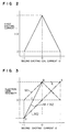
- This controller unit 6 controls the exciting currents I1 and I2 in such a fashion that the sum of their absolute values becomes substantially constant.
- Fig. 2 shows the relationship between these currents I1 and I2 in which the currents I2 is standardized by their maximum intensity.
- Fig. 3 shows the effective intensity of an electron lens by means of superimposition of the currents I1 and I2 versus the current I2.
- a one-dot-chain line M1 represents a first electron lens intensity which is generated only by the first exciting coil 2 with the current I1.
- a two-dot chain line M2 represents a second electron lens intensity which is generated only by the second exciting coil 2 with the current I2.
- a solid line represents the effective intensity of the electron lens, that is, it shows the sum of the first and second intensity of the two coils 1 and 2.
- the characteristics of the electron lens is as follows. At a portion A-B of the solid line, at which the electron lens intensity is constant, the currents I1 and I2 applied to the respective coils 1 and 2 have the same polarity.
- the currents I1 and I2 have the opposite polarity to each other.
- the electron lens intensity changes on proportion to the ratio of the currents I1 and I2.
- Negative lens intensity in Fig. 3 means that the rotating direction of an image becomes opposite. This phenomenon is appeared at the same time of the lens' focusing operation.
- the intensity of the electron lens can be changed from zero to the maximum value (+1) while the sum of the absolute values of the currents flowing through the same magnetic path is kept constant.
- Points C and E in Fig. 3 represent significant operational points of the lens of the present example.
- the currents I1 and I2 have the same absolute value.
- the currents have opposite polarity to each other so that the magnetic fields generated by the two exciting coils 1 and 2 offset each other, and lens intensity becomes zero when the intensity of the electron lens is considered as a whole.
- the magnetic field generated by the two coils are superimposed to each other so that the lens action, which is two times stronger than the single coil, can be obtained.
- Fig. 4 shows an embodiment of the present invention.
- a common exciting coil driving power supply 7 is used and the direction of the current I2 flowing through the second exciting coils 2 is switched by a polarity switch apparatus 8 as shown in the figure, the electron lens can easily be turned ON and OFF.
- the number of turns of the first and second exciting coils 1 and 2 is the same.
- the exciting coils 1 and 2 have the same turning direction.
- a magnetic field of the lens depends on both the turning direction and the polarity of exciting current. Accordingly, when one of coils has the opposite turning direction, the polarity of the exciting current applied to the coil should be turned so as to adapt also the above description.
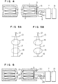
- Figs. 5A and 5B show an application example of the electron lens having the construction described above to a transmission electron microscope.
- an angular aperture of the electron beam emitted from an electron source 12 is limited by an aperture stop 13, and the electron beam is then irradiated on a specimen 16 through first and second converging lenses 14 and 15.
- the electron beam 17 is irradiated under the expanded state to the specimen 16 as shown in Fig. 5A to obtain a transmission image of this specimen.
- a portion (a very small portion) to be analyzed is determined in the image obtained in this way, and a thinly contracted electron beam is then irradiated to this portion (see Fig. 5B).
- Secondary data generated from this portion such as secondary electrons, X-rays, etc., are detected by a known detector, and useful data such as data of compositions, crystalline structures, etc., can be obtained.
- the electron lenses 14 and 15 constitute a condenser group of the electron beam irradiation system.
- the electron lens of this embodiment shown in Fig. 4 is used as the electron lens 15.
- the OFF state of this electron lens 15 is shown in Fig. 5A and its ON state, in Fig. 5B.
- the switch 8 makes the ON/OFF control of the electron lens 15.
- the controller 19 controls the power supply 7 at the time of switching of the switch 8 and makes the currents applied to the coils 1 and 2 temporarily (approximately for a second) zero.
- the coils 1 and 2 of the electron lens used in this embodiment have the number of turns of 560, and a current of 2.3 A is applied.
- the dimensions of the coils 1, 2 and the magnetic path 3 are substantially the same as those of an electron microscope (type HF-2000) produced by HITACHI, Ltd., the assigner of the present application.
- Fig. 6 shows an electron lens 20 according to another embodiment of the present invention.
- Like reference numerals are used in this drawing to identify like constituents as in Fig. 4, and the repetition of explanation of such constituents will be omitted.
- first exciting coil 1 and the second exciting coil 2 are connected in series.
- second and third exciting coils 22 and 23 are connected in parallel with the first exciting coil 21.
- These first to third exciting coils have the same number of turns.
- the turning direction of the first exciting coil is the same as that of the second exciting coil but is opposite to that of the third exciting coil.
- a switch 28 selectively connects one of the second and third exciting coils to the power supply 7. A current is always applied from the power supply 7 to the first exciting coil 21.
- the switch 28 selects the exciting coil 22
- the electron lens 20 is turned ON and the intensity of the electron lens is expressed by the sum of the magnetic fields generated by the first and second exciting coils.
- the switch 28 selects the third exciting coil 23
- the magnetic field generated by the first exciting coil 21 offsets the magnetic field generated by the third exciting coil 23, so that the electron lens 20 is turned OFF.
- the construction of the present invention when the construction of the present invention is applied to the second converging lens 15, only the lens intensity can be changed (ON/OFF) while the exciting current of the second converging lens 15 is kept constant. Accordingly, the second converging lens 15 is now substantially free from the temperature drift and can exhibit stable performance.
- the electron lens disclosed in each of the foregoing embodiments can be used as the electron lens of an electron microscope having the construction shown in Fig. 7.
- the electron lens is preferably used as a condenser lens 102 of the electron beam irradiation system or an image forming lens 103.
- the construction of the electron microscope shown in Fig. 7 refer to U.S. Patent Specification No. 4,788,425.
- the electron lens disclosed in each of the foregoing embodiments can further be applied to the electron microscopes described in U.S. Patent Specification Nos. 4,945,237 and 5,144,129.
- the electron lens of each of the foregoing embodiments can further be applied to an ion beam apparatus, an electron beam apparatus (EB), and so forth.
- EB electron beam apparatus
Landscapes
- Physics & Mathematics (AREA)
- Electromagnetism (AREA)
- Chemical & Material Sciences (AREA)
- Analytical Chemistry (AREA)
- Electron Beam Exposure (AREA)
- Electron Sources, Ion Sources (AREA)
Claims (7)
- Lentille électronique, comprenant :caractérisée en ce queune première bobine excitatrice (1),une seconde bobine excitatrice (2) ayant sensiblement le même nombre de spires que la première bobine excitatrice,un boítier (3) pour loger lesdites bobines excitatrices (1, 2),une alimentation électrique (7) etun moyen de commande d'excitation pour commander un état d'excitation desdites bobines excitatrices,
ledit moyen de commande d'excitation comprend un commutateur (8) et une première borne de ladite première bobine excitatrice (1) est connectée à ladite alimentation électrique (7), l'autre borne de ladite première bobine excitatrice (1) est connectée de manière sélective à l'une ou l'autre des bornes de ladite seconde bobine excitatrice (2) par ledit commutateur (8), et ledit commutateur connecte l'autre, respective, des bornes de ladite seconde bobine excitatrice (2) à ladite alimentation électrique (7) de façon que lesdites première et seconde bobines excitatrices soient excitées, leurs champs magnétiques se renforçant l'un l'autre lorsque ledit commutateur est dans un premier état, et leurs champs magnétiques se compensant l'un l'autre lorsque ledit commutateur est dans un second état. - Lentille électronique, comprenant :caractérisée en ce queune première bobine excitatrice (21),une seconde bobine excitatrice (22) ayant sensiblement le même nombre de spires que la première bobine excitatrice,un boítier (3) pour loger lesdites bobines excitatrices (21, 22),une alimentation électrique (7) etun moyen de commande d'excitation pour commander un état d'excitation desdites bobines excitatrices (21, 22),ledit moyen de commande d'excitation comprend un commutateur (28),une troisième bobine excitatrice (23) est disposée dans ledit boítier (3), etlesdites première et seconde bobines excitatrices (21, 22) ont des spires orientées dans le même sens, ladite troisième bobine excitatrice (23) a sensiblement le même nombre de spires que ladite première bobine excitatrice (21) mais des spires orientées dans un sens différent, lesdites seconde et troisième bobines excitatrices (22, 23) sont montées en parallèle avec ladite première bobine excitatrice (21) et ledit moyen de commande d'excitation excite toujours ladite première bobine excitatrice (21) tandis qu'il excite de manière sélective l'une ou l'autre desdites seconde et troisième bobines excitatrices (22, 23) à l'aide dudit commutateur (28), de telle sorte que lesdites première et seconde bobines excitatrices (21, 22) sont excitées, leurs champs magnétiques se renforçant l'un l'autre lorsque ledit commutateur est dans un premier état et lesdites première et troisième bobines excitatrices (21, 23) sont excitées, leurs champs magnétiques se compensant sensiblement l'un l'autre lorsque ledit commutateur est dans un second état.
- Lentille électronique selon la revendication 1 ou 2, comprenant en outre
un moyen (19) pour arrêter temporairement ladite alimentation électrique (7) en électricité lors du basculement dudit commutateur (8, 28). - Microscope électronique, comprenantun canon (12, 13) à électrons,une platine porte-échantillon, etune lentille électronique (14, 15) selon l'une quelconque des revendications 1 à 3.
- Dispositif de projection de faisceau d'électrons équipé d'une lentille électronique selon l'une quelconque des revendications 1 à 3.
- Dispositif selon la revendication 4 ou 5, dans lequel ladite lentille électronique est utilisée comme lentille de condenseur.
- Dispositif selon la revendication 4 ou 5, dans lequel ladite lentille électronique est utilisée comme lentille de projection.
Applications Claiming Priority (3)
| Application Number | Priority Date | Filing Date | Title |
|---|---|---|---|
| JP32148392 | 1992-11-06 | ||
| JP321483/92 | 1992-11-06 | ||
| JP32148392 | 1992-11-06 |
Publications (2)
| Publication Number | Publication Date |
|---|---|
| EP0596529A1 EP0596529A1 (fr) | 1994-05-11 |
| EP0596529B1 true EP0596529B1 (fr) | 2002-02-27 |
Family
ID=18133072
Family Applications (1)
| Application Number | Title | Priority Date | Filing Date |
|---|---|---|---|
| EP93117996A Expired - Lifetime EP0596529B1 (fr) | 1992-11-06 | 1993-11-05 | Lentille électronique |
Country Status (3)
| Country | Link |
|---|---|
| US (1) | US5442182A (fr) |
| EP (1) | EP0596529B1 (fr) |
| DE (1) | DE69331620T2 (fr) |
Families Citing this family (10)
| Publication number | Priority date | Publication date | Assignee | Title |
|---|---|---|---|---|
| US6523240B1 (en) | 1996-05-09 | 2003-02-25 | Spotless Plastics Pty. Ltd. | Method for reusing hangers with size indicia |
| US6627899B2 (en) * | 1998-05-27 | 2003-09-30 | Nikon Corporation | Magnetic lenses, charged-particle-beam optical systems, and charged-particle-beam pattern-transfer apparatus |
| JP2002117800A (ja) * | 2000-10-05 | 2002-04-19 | Jeol Ltd | 電子線バイプリズム装置を備えた電子顕微鏡 |
| US6624426B2 (en) * | 2000-12-11 | 2003-09-23 | Schlumberger Technologies Inc. | Split magnetic lens for controlling a charged particle beam |
| US7078994B2 (en) * | 2003-02-18 | 2006-07-18 | Glenn Henry Martin | Constant power and temperature coil |
| DE102004019835B4 (de) * | 2004-04-23 | 2007-08-02 | Vistec Electron Beam Gmbh | Beleuchtungskondensor für ein Partikeloptik-Projektionssystem |
| JP6285753B2 (ja) * | 2014-02-28 | 2018-02-28 | 日本電子株式会社 | 透過電子顕微鏡 |
| CN106783492A (zh) * | 2016-12-14 | 2017-05-31 | 聚束科技(北京)有限公司 | 一种磁透镜及激励电流控制方法 |
| JP2019169362A (ja) * | 2018-03-23 | 2019-10-03 | 株式会社日立製作所 | 電子ビーム装置 |
| JP6954885B2 (ja) * | 2018-11-26 | 2021-10-27 | 日本電子株式会社 | 荷電粒子線装置及び荷電粒子線装置の制御方法 |
Family Cites Families (7)
| Publication number | Priority date | Publication date | Assignee | Title |
|---|---|---|---|---|
| US2323328A (en) * | 1940-10-31 | 1943-07-06 | Rca Corp | Projection lens for electron microscopes |
| US2418349A (en) * | 1945-12-13 | 1947-04-01 | Rca Corp | Method of and means for correcting for distortion in electron lens systems |
| NL6918302A (fr) * | 1969-12-05 | 1971-06-08 | ||
| JPS5213713B2 (fr) * | 1971-12-15 | 1977-04-16 | ||
| US4345152A (en) * | 1980-08-11 | 1982-08-17 | The Perkin-Elmer Corporation | Magnetic lens |
| JPS5981850A (ja) * | 1982-11-02 | 1984-05-11 | Internatl Precision Inc | 電子レンズ |
| US4544847A (en) * | 1983-07-28 | 1985-10-01 | Varian Associates, Inc. | Multi-gap magnetic imaging lens for charged particle beams |
-
1993
- 1993-11-03 US US08/145,161 patent/US5442182A/en not_active Expired - Lifetime
- 1993-11-05 DE DE69331620T patent/DE69331620T2/de not_active Expired - Lifetime
- 1993-11-05 EP EP93117996A patent/EP0596529B1/fr not_active Expired - Lifetime
Also Published As
| Publication number | Publication date |
|---|---|
| DE69331620D1 (de) | 2002-04-04 |
| DE69331620T2 (de) | 2002-10-17 |
| EP0596529A1 (fr) | 1994-05-11 |
| US5442182A (en) | 1995-08-15 |
Similar Documents
| Publication | Publication Date | Title |
|---|---|---|
| US4306149A (en) | Electron microscope (comprising an auxiliary lens) | |
| US7872240B2 (en) | Corrector for charged-particle beam aberration and charged-particle beam apparatus | |
| US6852983B2 (en) | Charged-particle beam apparatus equipped with aberration corrector | |
| EP0596529B1 (fr) | Lentille électronique | |
| JP2000500913A (ja) | 粒子光学機器の色収差を補正する補正装置 | |
| US3851172A (en) | Compound electron lens for electron microscope and the like | |
| JP3899317B2 (ja) | 粒子ビーム装置のための偏向システム | |
| EP0133016A2 (fr) | Lentille magnétique à intervalles multiples par la focalisation des faisceaux de particules chargées | |
| US4469948A (en) | Composite concentric-gap magnetic lens | |
| JP2007280966A (ja) | 電子光学レンズ装置 | |
| EP0179294A1 (fr) | Dispositif à faisceau ionique avec micro-rayon | |
| US4105890A (en) | Device for electron-beam heating of materials | |
| JPH10177952A (ja) | 電子線を用いた転写装置 | |
| JPH01319236A (ja) | 電界放射電子銃 | |
| EP0551027B1 (fr) | Appareil à focalisation magnétique | |
| JP3234373B2 (ja) | 磁界形電子レンズおよびこれを用いた電子線装置 | |
| US6049084A (en) | Charged-particle-beam optical system | |
| US4520264A (en) | Electron microscope | |
| EP0493028A2 (fr) | Laser à gaz avec un dispositif d'excitation par décharge | |
| US4450357A (en) | Electron lens equipped with three magnetic pole pieces | |
| JPS5810818B2 (ja) | 電磁レンズ装置 | |
| JPH05128986A (ja) | 磁場型レンズ | |
| EP4362055A2 (fr) | Microscope électronique, élément multipolaire à utiliser dans celui-ci et procédé de commande pour un tel microscope électronique | |
| JP2876280B2 (ja) | ビーム発生方法及び装置 | |
| JP2004199912A (ja) | 荷電粒子ビーム装置における収差補正装置 |
Legal Events
| Date | Code | Title | Description |
|---|---|---|---|
| PUAI | Public reference made under article 153(3) epc to a published international application that has entered the european phase |
Free format text: ORIGINAL CODE: 0009012 |
|
| AK | Designated contracting states |
Kind code of ref document: A1 Designated state(s): DE NL |
|
| 17P | Request for examination filed |
Effective date: 19941013 |
|
| 17Q | First examination report despatched |
Effective date: 19951121 |
|
| GRAG | Despatch of communication of intention to grant |
Free format text: ORIGINAL CODE: EPIDOS AGRA |
|
| GRAG | Despatch of communication of intention to grant |
Free format text: ORIGINAL CODE: EPIDOS AGRA |
|
| GRAH | Despatch of communication of intention to grant a patent |
Free format text: ORIGINAL CODE: EPIDOS IGRA |
|
| GRAH | Despatch of communication of intention to grant a patent |
Free format text: ORIGINAL CODE: EPIDOS IGRA |
|
| GRAA | (expected) grant |
Free format text: ORIGINAL CODE: 0009210 |
|
| AK | Designated contracting states |
Kind code of ref document: B1 Designated state(s): DE NL |
|
| REF | Corresponds to: |
Ref document number: 69331620 Country of ref document: DE Date of ref document: 20020404 |
|
| PLBE | No opposition filed within time limit |
Free format text: ORIGINAL CODE: 0009261 |
|
| STAA | Information on the status of an ep patent application or granted ep patent |
Free format text: STATUS: NO OPPOSITION FILED WITHIN TIME LIMIT |
|
| 26N | No opposition filed |
Effective date: 20021128 |
|
| PGFP | Annual fee paid to national office [announced via postgrant information from national office to epo] |
Ref country code: DE Payment date: 20121031 Year of fee payment: 20 |
|
| PGFP | Annual fee paid to national office [announced via postgrant information from national office to epo] |
Ref country code: NL Payment date: 20121116 Year of fee payment: 20 |
|
| REG | Reference to a national code |
Ref country code: DE Ref legal event code: R071 Ref document number: 69331620 Country of ref document: DE |
|
| REG | Reference to a national code |
Ref country code: NL Ref legal event code: V4 Effective date: 20131105 |
|
| PG25 | Lapsed in a contracting state [announced via postgrant information from national office to epo] |
Ref country code: DE Free format text: LAPSE BECAUSE OF EXPIRATION OF PROTECTION Effective date: 20131106 |