EP0596584A2 - Arrangement de saisie de perturbation - Google Patents
Arrangement de saisie de perturbation Download PDFInfo
- Publication number
- EP0596584A2 EP0596584A2 EP93250297A EP93250297A EP0596584A2 EP 0596584 A2 EP0596584 A2 EP 0596584A2 EP 93250297 A EP93250297 A EP 93250297A EP 93250297 A EP93250297 A EP 93250297A EP 0596584 A2 EP0596584 A2 EP 0596584A2
- Authority
- EP
- European Patent Office
- Prior art keywords
- fault detection
- electronic assembly
- detection according
- coupling
- sensor
- Prior art date
- Legal status (The legal status is an assumption and is not a legal conclusion. Google has not performed a legal analysis and makes no representation as to the accuracy of the status listed.)
- Granted
Links
Images


Classifications
-
- G—PHYSICS
- G01—MEASURING; TESTING
- G01R—MEASURING ELECTRIC VARIABLES; MEASURING MAGNETIC VARIABLES
- G01R31/00—Arrangements for testing electric properties; Arrangements for locating electric faults; Arrangements for electrical testing characterised by what is being tested not provided for elsewhere
- G01R31/28—Testing of electronic circuits, e.g. by signal tracer
Definitions
- the invention relates to a device for fault detection of the type specified in the preamble of claim 1.
- line-conducted interference levels caused by line-bound and / or line-unbound disturbances are one of the main causes for influencing the electromagnetic compatibility of electronic control and regulation assemblies or the failure for the operational management of essential system parts.
- Line-related faults are recorded in a known manner in that a fuse responds and causes a permanent line interruption.
- the triggering of the fuse also forms a fault indicator, combined with switching off the correspondingly protected module for safety reasons. After the cause of the fault has been eliminated, the fuse is then replaced or switched on again.
- the fuse itself provides indirect information about the cause of the fault.
- registration devices for (exclusively line-bound) faults are known, which - particularly in the area of the electricity supply companies - continuously register spikes occurring on lines in order to be able to narrow down the cause of the fault in the event of failures.
- a circuit arrangement is known from DD-PS 279 083, with which digital modules can be tested with regard to their electromagnetic immunity.
- the clock or set input of a flip-flop which should have the same or similar interference behavior as the components of the module to be checked, is connected to a galvanically tapped interference voltage that arises in the test object as a result of electromagnetic interference.
- the main disadvantage of the solution described above is that the response of the flip-flop to possible interference pulses is equated with the interference pulse compatibility of digital circuits of any structure. With a few exceptions, this involves incorrect assessments that can lead to considerable damage to the device. In addition, the interference potentials are tapped across the spatial diagonal of the device, which makes a more precise fault analysis much more difficult, and that the sensitivity of the circuit for fault registration must be below the level of damage leading to damage in order to Ensure registration.
- the invention has for its object to provide a device of the type mentioned, which makes it possible in the case of line-borne, caused by line-bound and / or line-bound interference signals, after a malfunction, a more accurate statement both about to hit the amplitude of the interference signal as well as its possible cause.
- This task differs fundamentally, for example, from that on which a circuit arrangement known from DD 279 083 AI is based, for the clock or set input of a flip-flop, which is supposed to show the same or similar interference behavior as the components of the module to be tested, with the tapped interference voltage is connected.
- This circuit is not used to discriminate a disturbance occurring during operation, but to check the electromagnetic shielding of the device in question, by trying to determine the influence of a test module by introducing a disturbance in order to then draw conclusions about the behavior of other modules.
- the invention is based on the knowledge that the predominant number of line-bound and line-bound interferences which impair the electromagnetic compatibility between different electrical or electronic assemblies of devices are transmitted as interference levels through lines to the assemblies. Likewise, it should be noted that a fixed assignment between the device for fault monitoring and the module to be monitored is particularly advantageous for evidence-securing fault detection. This ensures that the location and type of disruption can be concluded at any time.
- a recognized and registered fault is not subsequently changed by the further signal processing by the electronic circuit of the module to be monitored. Since the assembly is likely to be affected by the malfunction in its operation, the malfunction message would also be handled incorrectly with a high probability, so that its reliability is questioned.
- a line-based fault is detected on an input line of the electronic assembly to be monitored.
- the coupling of the device for interference detection is carried out with a fixed spatial assignment to the assembly in a very small space in order to minimize falsification of the detected interference level.
- the use of a threshold circuit advantageously ensures level monitoring on the input line, so that any disturbance which leads to the logic level being exceeded can be detected and locally assigned.
- connection of the device for fault detection to the input line of a module to be monitored is established by a non-galvanic connection.
- a capacitive or inductive coupling advantageously prevents the normal logic level from being falsified and also allows operation on electrically isolated systems.
- the threshold value transmitter arranged upstream of the sensor / memory element is designed as a voltage divider.
- the adjustable or preprogrammable division ratio of one or more voltage dividers preferably connected in parallel, enables a simple implementation of different potentials caused by the disturbances, which are adapted to corresponding responsivities of the storage-capable detection devices, preferably bistable flip-flops, arranged downstream of the respective voltage dividers are.
- an additional evaluation unit e.g. Microcomputers, into which the disturbances detected by the sensor / memory elements are fed, can thus be compared to disturbance levels of different strengths and can be assigned to possible disturbances.
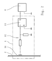
- the device for fault detection 1 shown in FIG. 1 as a block diagram is connected by a coupling element 3 to a line 2 of an electronic circuit to be monitored with regard to line-bound and / or line-free faults.
- the voltage values, corresponding to a fault, transmitted by the coupling to the line 2 to a threshold value transmitter, are fed to a sensor / memory element 5 and are suitably detected there.
- the detection and evaluation of detected malfunction events is advantageously carried out in a computer-assisted manner in an evaluation unit 6 connected downstream of the sensor / memory element 5.
- the effective relationship between the cable run 2 and the device for fault detection 1 is realized in accordance with the circuit diagram shown schematically in FIG. 2 by a capacitive coupling point 14, a section of the cable run 2 forming one of the electrodes of the capacitor of the coupling point.
- the threshold value transmitter (position 4 in FIG. 1) is designed as a voltage divider 12, the division ratio of which is adapted to the response threshold at the setting input S of the bistable multivibrator 13.
- the fault states detected and temporarily stored by the bistable flip-flop 13, preferably a flip-flop, are detected and further processed at the signal output Q of the bistable flip-flop 13 by the evaluation unit 6 (e.g. reference to comparison values of known disturbance events and registration of the disturbance amplitudes)
- the coupling 14 to one of the cable runs 2 of the electronic assembly is also capacitive.
- This capacitive coupling of a device 1 for fault detection can be carried out simultaneously at different points in the electronic assembly and at the same time - with suitable dimensioning of the capacitance of the coupling capacitor used - enables operation on electrically isolated systems.
- the device for fault detection 1 shown in FIG. 4 as a circuit diagram has an inductive coupling point 15 for coupling the voltage divider 12.
- the coupling point 15 is advantageously designed as a transformer, the line 2 forming the primary winding of the transformer.
- the operation of the rest of the circuit corresponds to the statements made above.
- FIG. 5 schematically shows an electronic assembly 7 to be monitored with the associated device 1 for fault detection in a perspective representation.
- the device 1 for fault detection is arranged on the circuit board 8 in the immediate vicinity of the plug 10.
- the detail A covers the area of the coupling point, which is located directly on the connector pin 11 or on the associated solder pad 9 of a cable line, preferably an input line of the electronic assembly 7 on the printed circuit board 8.
- the elements 3, 4, 5 of the device 1 thus form a structural unit with the closest spatial association with the electronic assembly 7.
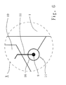
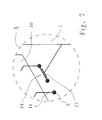
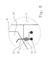
- FIGS. 6, 7 and 8 show, as an enlargement of the detail A in FIG. 5, a schematic representation of various embodiments of the coupling points 14 and 15 of the device 1 for fault detection, the formation of which advantageously includes a section of a line of the electronic assembly to be monitored.
- FIG. 6 shows a capacitive coupling point 14, the capacitor of which consists of an electrode 16 which surrounds the soldering eye 9 of the connector pin 11 in a ring and a rod electrode formed from the connector pin 11.
- the connector pin 11 led out of the connector 10 is preferably connected to an input line of the electronic assembly.
- the capacitance of the coupling point 14 can also be formed in a simple manner from two parallel and closely arranged cable runs 17, one of which embodies a section of the input line of the electronic assembly, as shown schematically in FIG.
- FIG. 8 shows an exemplary embodiment of an inductive coupling 15 of the device for fault detection 1 to a line of the electronics assembly.
- the coupling point 15 consists of a transformer, the primary winding of which is formed from the plug pin 11.
- the interference amplitudes are transmitted to the secondary winding 18 by induction and can then be further processed in the device for interference detection 1, as previously explained.
- insulation (not shown) is provided between plug pin 11 and the secondary winding 18 surrounding it.
- the embodiment of the invention is not limited to the preferred exemplary embodiment specified above. Rather, a number of variants are conceivable which make use of the solution shown, even in the case of fundamentally different types.
Landscapes
- Engineering & Computer Science (AREA)
- General Engineering & Computer Science (AREA)
- Physics & Mathematics (AREA)
- General Physics & Mathematics (AREA)
- Testing Electric Properties And Detecting Electric Faults (AREA)
- Testing Of Short-Circuits, Discontinuities, Leakage, Or Incorrect Line Connections (AREA)
- Acyclic And Carbocyclic Compounds In Medicinal Compositions (AREA)
- Chair Legs, Seat Parts, And Backrests (AREA)
- Bidet-Like Cleaning Device And Other Flush Toilet Accessories (AREA)
- Air Bags (AREA)
- Maintenance And Inspection Apparatuses For Elevators (AREA)
- Application Of Or Painting With Fluid Materials (AREA)
Applications Claiming Priority (2)
| Application Number | Priority Date | Filing Date | Title |
|---|---|---|---|
| DE4237828A DE4237828C2 (de) | 1992-11-04 | 1992-11-04 | Einrichtung zur Störungserfassung |
| DE4237828 | 1992-11-04 |
Publications (3)
| Publication Number | Publication Date |
|---|---|
| EP0596584A2 true EP0596584A2 (fr) | 1994-05-11 |
| EP0596584A3 EP0596584A3 (fr) | 1995-03-15 |
| EP0596584B1 EP0596584B1 (fr) | 1999-03-17 |
Family
ID=6472463
Family Applications (1)
| Application Number | Title | Priority Date | Filing Date |
|---|---|---|---|
| EP93250297A Expired - Lifetime EP0596584B1 (fr) | 1992-11-04 | 1993-11-03 | Arrangement de saisie de perturbation |
Country Status (3)
| Country | Link |
|---|---|
| EP (1) | EP0596584B1 (fr) |
| AT (1) | ATE177845T1 (fr) |
| DE (2) | DE4237828C2 (fr) |
Families Citing this family (3)
| Publication number | Priority date | Publication date | Assignee | Title |
|---|---|---|---|---|
| DE4417031C1 (de) * | 1994-05-14 | 1995-08-17 | Gunter Dipl Ing Langer | Verfahren zur Bewertung der EMV-Eigenschaften von integrierten Schaltungen und Anordnung zur Durchführung des Verfahrens |
| DE10151824B4 (de) * | 2001-10-15 | 2006-07-27 | Langer, Gunter, Dipl.-Ing. | Verfahren zur Ermittlung der elektromagnetischen Störaussendung einer Elektronikbaugruppe |
| DE102012012115A1 (de) * | 2012-06-20 | 2013-12-24 | Robert Bosch Gmbh | Verfahren zur Erkennung von elektromagnetischen Strörinpulsen und Elektronikbauteil zur Durchführung des Verfahrens |
Family Cites Families (6)
| Publication number | Priority date | Publication date | Assignee | Title |
|---|---|---|---|---|
| US3746981A (en) * | 1971-09-24 | 1973-07-17 | Collins Radio Co | Electrical fault monitoring with memory |
| DE3639430C1 (en) * | 1986-11-18 | 1988-02-04 | Ernst Neubert | Circuit arrangement to protect computers |
| US5025344A (en) * | 1988-11-30 | 1991-06-18 | Carnegie Mellon University | Built-in current testing of integrated circuits |
| DD279083A1 (de) * | 1988-12-29 | 1990-05-23 | Buchwitz Otto Starkstrom | Schaltungsanordnung zur pruefung der elektromagnetischen stoerfestigkeit digitaler baugruppen |
| JPH0390872A (ja) * | 1989-09-01 | 1991-04-16 | Toshiba Corp | 半導体装置 |
| DE4115432A1 (de) * | 1991-05-08 | 1992-11-12 | Eac Automation Consult Gmbh | Schaltung zur stoerungserfassung fuer eine prozessorgesteuerte elektronische baugruppe |
-
1992
- 1992-11-04 DE DE4237828A patent/DE4237828C2/de not_active Expired - Fee Related
-
1993
- 1993-11-03 AT AT93250297T patent/ATE177845T1/de not_active IP Right Cessation
- 1993-11-03 EP EP93250297A patent/EP0596584B1/fr not_active Expired - Lifetime
- 1993-11-03 DE DE59309455T patent/DE59309455D1/de not_active Expired - Fee Related
Also Published As
| Publication number | Publication date |
|---|---|
| DE4237828A1 (de) | 1994-05-05 |
| EP0596584A3 (fr) | 1995-03-15 |
| DE4237828C2 (de) | 1996-08-01 |
| EP0596584B1 (fr) | 1999-03-17 |
| DE59309455D1 (de) | 1999-04-22 |
| ATE177845T1 (de) | 1999-04-15 |
Similar Documents
| Publication | Publication Date | Title |
|---|---|---|
| DE112010004351B4 (de) | Elektrischer Schaltkreis mit Überspannungsschutz-Überwachungseinrichtung | |
| DE112007001098B4 (de) | Ethernet-Datensignal-Isolationsvorrichtung | |
| EP4046256B1 (fr) | Circuit d'unité de commande pour véhicule automobile, véhicule automobile et procédé de fonctionnement du circuit d'unité de commande | |
| EP2378663B1 (fr) | Circuit d'entrée sécurisé doté d'un raccordement périphérique sur un canal unique pour l'entrée d'un utilisateur de bus | |
| WO2013024151A1 (fr) | Élément de base pour supporter un module de protection contre les surtensions et système de bus modulaire | |
| DE2852582C2 (fr) | ||
| DE102007006219A1 (de) | Stromsensoranordnung | |
| DE102005016127A1 (de) | Sensorsystem | |
| EP0596584B1 (fr) | Arrangement de saisie de perturbation | |
| EP0609261B1 (fr) | Systeme de controle d'un systeme de commande electrique | |
| DE3519252A1 (de) | Fehlersichere logikschaltung | |
| EP0513952B1 (fr) | Circuit de détection de défaillance pour un ensemble électronique | |
| DE10033073A1 (de) | Verfahren zur Fehleraufdeckung an sicherheitsgerichteten Sensoren | |
| EP0164511A1 (fr) | Circuit de contrôle pour détecter le dépassement des valeurs limites données | |
| DE4313230C2 (de) | Überwachungsschaltung für den Funktionszustand der Signalleitungen einer Differenzsignal-Übertragungsstrecke | |
| EP0254125A1 (fr) | Système de signalisation de dangers | |
| DE19847841A1 (de) | Vorrichtung zur Identifizierung und Funktionsüberprüfung von Sensoren | |
| EP0958985B1 (fr) | Montage pour la surveillance de données opérationnelles de systèmes de signalisation de sécurité ferroviaires | |
| DE3931539A1 (de) | Anordnung zum anschluss von endgeraeten an eine busleitung | |
| DE102014116188A1 (de) | System zum fehlersicheren Abschalten eines elektrischen Verbrauchers | |
| EP4316945B1 (fr) | Dispositif de transmission de signal d'une installation technique de sécurité de signal destiné à la transmission sécurisée d'un signal de courant alternatif | |
| WO1998026299A1 (fr) | Dispositif de detection d'etat de n condensateurs de puissance appartenant a un groupe de condensateurs haute tension | |
| EP0372256B1 (fr) | Procédé de protection d'un transformateur et dispositif de mise en oeuvre du procédé | |
| DE102008008047A1 (de) | Externer Watchdog sowie Schaltgerät, insbesondere Niederspannungsschaltgerät, mit einem externen Watchdog | |
| DE2703255A1 (de) | Sicherungseinrichtung fuer eine verbraucheranordnung |
Legal Events
| Date | Code | Title | Description |
|---|---|---|---|
| PUAI | Public reference made under article 153(3) epc to a published international application that has entered the european phase |
Free format text: ORIGINAL CODE: 0009012 |
|
| AK | Designated contracting states |
Kind code of ref document: A2 Designated state(s): AT CH DE FR GB IE IT LI SE |
|
| PUAL | Search report despatched |
Free format text: ORIGINAL CODE: 0009013 |
|
| AK | Designated contracting states |
Kind code of ref document: A3 Designated state(s): AT CH DE FR GB IE IT LI SE |
|
| 17P | Request for examination filed |
Effective date: 19950830 |
|
| 17Q | First examination report despatched |
Effective date: 19970526 |
|
| GRAG | Despatch of communication of intention to grant |
Free format text: ORIGINAL CODE: EPIDOS AGRA |
|
| GRAG | Despatch of communication of intention to grant |
Free format text: ORIGINAL CODE: EPIDOS AGRA |
|
| GRAH | Despatch of communication of intention to grant a patent |
Free format text: ORIGINAL CODE: EPIDOS IGRA |
|
| RAP3 | Party data changed (applicant data changed or rights of an application transferred) |
Owner name: EAC AUTOMATION-CONSULTING-GMBH |
|
| GRAH | Despatch of communication of intention to grant a patent |
Free format text: ORIGINAL CODE: EPIDOS IGRA |
|
| GRAA | (expected) grant |
Free format text: ORIGINAL CODE: 0009210 |
|
| AK | Designated contracting states |
Kind code of ref document: B1 Designated state(s): AT CH DE FR GB IE IT LI SE |
|
| PG25 | Lapsed in a contracting state [announced via postgrant information from national office to epo] |
Ref country code: SE Free format text: THE PATENT HAS BEEN ANNULLED BY A DECISION OF A NATIONAL AUTHORITY Effective date: 19990317 Ref country code: IT Free format text: LAPSE BECAUSE OF FAILURE TO SUBMIT A TRANSLATION OF THE DESCRIPTION OR TO PAY THE FEE WITHIN THE PRE;WARNING: LAPSES OF ITALIAN PATENTS WITH EFFECTIVE DATE BEFORE 2007 MAY HAVE OCCURRED AT ANY TIME BEFORE 2007. THE CORRECT EFFECTIVE DATE MAY BE DIFFERENT FROM THE ONE RECORDED.SCRIBED TIME-LIMIT Effective date: 19990317 |
|
| REF | Corresponds to: |
Ref document number: 177845 Country of ref document: AT Date of ref document: 19990415 Kind code of ref document: T |
|
| REG | Reference to a national code |
Ref country code: CH Ref legal event code: EP |
|
| REG | Reference to a national code |
Ref country code: IE Ref legal event code: FG4D Free format text: GERMAN |
|
| REF | Corresponds to: |
Ref document number: 59309455 Country of ref document: DE Date of ref document: 19990422 |
|
| GBT | Gb: translation of ep patent filed (gb section 77(6)(a)/1977) |
Effective date: 19990428 |
|
| REG | Reference to a national code |
Ref country code: CH Ref legal event code: NV Representative=s name: PATENTANWAELTE SCHAAD, BALASS, MENZL & PARTNER AG |
|
| ET | Fr: translation filed | ||
| PG25 | Lapsed in a contracting state [announced via postgrant information from national office to epo] |
Ref country code: IE Free format text: LAPSE BECAUSE OF NON-PAYMENT OF DUE FEES Effective date: 19991019 |
|
| PG25 | Lapsed in a contracting state [announced via postgrant information from national office to epo] |
Ref country code: GB Free format text: LAPSE BECAUSE OF NON-PAYMENT OF DUE FEES Effective date: 19991103 Ref country code: AT Free format text: LAPSE BECAUSE OF NON-PAYMENT OF DUE FEES Effective date: 19991103 |
|
| REG | Reference to a national code |
Ref country code: IE Ref legal event code: FD4D |
|
| PG25 | Lapsed in a contracting state [announced via postgrant information from national office to epo] |
Ref country code: LI Free format text: LAPSE BECAUSE OF NON-PAYMENT OF DUE FEES Effective date: 19991130 Ref country code: CH Free format text: LAPSE BECAUSE OF NON-PAYMENT OF DUE FEES Effective date: 19991130 |
|
| PLBE | No opposition filed within time limit |
Free format text: ORIGINAL CODE: 0009261 |
|
| 26N | No opposition filed | ||
| GBPC | Gb: european patent ceased through non-payment of renewal fee |
Effective date: 19991103 |
|
| REG | Reference to a national code |
Ref country code: CH Ref legal event code: PL |
|
| PG25 | Lapsed in a contracting state [announced via postgrant information from national office to epo] |
Ref country code: FR Free format text: LAPSE BECAUSE OF NON-PAYMENT OF DUE FEES Effective date: 20000731 |
|
| REG | Reference to a national code |
Ref country code: FR Ref legal event code: ST |
|
| PGFP | Annual fee paid to national office [announced via postgrant information from national office to epo] |
Ref country code: DE Payment date: 20021204 Year of fee payment: 10 |
|
| PG25 | Lapsed in a contracting state [announced via postgrant information from national office to epo] |
Ref country code: DE Free format text: LAPSE BECAUSE OF NON-PAYMENT OF DUE FEES Effective date: 20040602 |