EP0596689B1 - Capteur magnétorésistif - Google Patents
Capteur magnétorésistif Download PDFInfo
- Publication number
- EP0596689B1 EP0596689B1 EP93308726A EP93308726A EP0596689B1 EP 0596689 B1 EP0596689 B1 EP 0596689B1 EP 93308726 A EP93308726 A EP 93308726A EP 93308726 A EP93308726 A EP 93308726A EP 0596689 B1 EP0596689 B1 EP 0596689B1
- Authority
- EP
- European Patent Office
- Prior art keywords
- layer
- layers
- ferromagnetic material
- magnetic
- magnetoresistive sensor
- Prior art date
- Legal status (The legal status is an assumption and is not a legal conclusion. Google has not performed a legal analysis and makes no representation as to the accuracy of the status listed.)
- Expired - Lifetime
Links
Images



Classifications
-
- B—PERFORMING OPERATIONS; TRANSPORTING
- B82—NANOTECHNOLOGY
- B82Y—SPECIFIC USES OR APPLICATIONS OF NANOSTRUCTURES; MEASUREMENT OR ANALYSIS OF NANOSTRUCTURES; MANUFACTURE OR TREATMENT OF NANOSTRUCTURES
- B82Y25/00—Nanomagnetism, e.g. magnetoimpedance, anisotropic magnetoresistance, giant magnetoresistance or tunneling magnetoresistance
-
- G—PHYSICS
- G11—INFORMATION STORAGE
- G11B—INFORMATION STORAGE BASED ON RELATIVE MOVEMENT BETWEEN RECORD CARRIER AND TRANSDUCER
- G11B5/00—Recording by magnetisation or demagnetisation of a record carrier; Reproducing by magnetic means; Record carriers therefor
- G11B5/127—Structure or manufacture of heads, e.g. inductive
- G11B5/33—Structure or manufacture of flux-sensitive heads, i.e. for reproduction only; Combination of such heads with means for recording or erasing only
- G11B5/39—Structure or manufacture of flux-sensitive heads, i.e. for reproduction only; Combination of such heads with means for recording or erasing only using magneto-resistive devices or effects
- G11B5/3903—Structure or manufacture of flux-sensitive heads, i.e. for reproduction only; Combination of such heads with means for recording or erasing only using magneto-resistive devices or effects using magnetic thin film layers or their effects, the films being part of integrated structures
-
- B—PERFORMING OPERATIONS; TRANSPORTING
- B82—NANOTECHNOLOGY
- B82Y—SPECIFIC USES OR APPLICATIONS OF NANOSTRUCTURES; MEASUREMENT OR ANALYSIS OF NANOSTRUCTURES; MANUFACTURE OR TREATMENT OF NANOSTRUCTURES
- B82Y10/00—Nanotechnology for information processing, storage or transmission, e.g. quantum computing or single electron logic
-
- G—PHYSICS
- G11—INFORMATION STORAGE
- G11B—INFORMATION STORAGE BASED ON RELATIVE MOVEMENT BETWEEN RECORD CARRIER AND TRANSDUCER
- G11B5/00—Recording by magnetisation or demagnetisation of a record carrier; Reproducing by magnetic means; Record carriers therefor
- G11B5/127—Structure or manufacture of heads, e.g. inductive
- G11B5/33—Structure or manufacture of flux-sensitive heads, i.e. for reproduction only; Combination of such heads with means for recording or erasing only
- G11B5/39—Structure or manufacture of flux-sensitive heads, i.e. for reproduction only; Combination of such heads with means for recording or erasing only using magneto-resistive devices or effects
- G11B2005/3996—Structure or manufacture of flux-sensitive heads, i.e. for reproduction only; Combination of such heads with means for recording or erasing only using magneto-resistive devices or effects large or giant magnetoresistive effects [GMR], e.g. as generated in spin-valve [SV] devices
Definitions
- the present invention relates generally to magnetic sensors for reading information signals recorded in a magnetic medium and, more particularly, to a magnetoresistive read sensor.
- the prior art discloses a magnetic read transducer referred to as a magnetoresistive (MR) sensor or head which has been shown to be capable of reading data from a magnetic surface at great linear densities.
- An MR sensor detects magnetic field signals through the resistance changes of a read element fabricated of a magnetic material as a function of the strength and direction of magnetic flux being sensed by the read element.
- These prior art MR sensors operate on the basis of the anisotropic magnetoresistive (AMR) effect in which a component of the read element resistance varies as the square of the cosine (cos 2 ) of the angle between the magnetization and the direction of sense current flow through the element.
- AMR anisotropic magnetoresistive
- U.S. Patent No. 4,949,039 to Grunberg describes a layered magnetic structure which yields enhanced MR effects caused by antiparallel alignment of the magnetizations in the magnetic layers.
- Grunberg lists ferromagnetic transition metals and alloys, but does not indicate preferred materials from the list for superior MR signal amplitude.
- Grunberg further describes the use of antiferromagnetic-type exchange coupling to obtain the antiparallel alignment in which adjacent layers of ferromagnetic materials are separated by a thin interlayer of chromium (Cr) or yttrium (Y).
- European Patent Application EP-A-490608 discloses an MR sensor in which the resistance between two uncoupled ferromagnetic layers is observed to vary as the cosine of the angle between the magnetizations of the two layers and which is independent of the direction of current flow through the sensor. This mechanism produces a magnetoresistance that, for selected combinations of materials, is greater in magnitude than the AMR, and is referred to as giant magnetoresistance or the "spin valve" (SV) magnetoresistance.
- SV spin valve
- Co-pending European Patent Application serial no 93306379.4 describes an MR sensor based on the above-described effect which includes two thin film layers of ferromagnetic material separated by a thin film layer of a non-magnetic metallic material and in which the magnetization of one ferromagnetic layer is maintained perpendicular to the magnetization of the other ferromagnetic layer at zero externally applied magnetic field by exchange coupling with an adjacent layer of antiferromagnetic material.
- a magnetoresistive sensor comprising a layered structure formed on a substrate, the structure comprising, a first, a second and a third layer of ferromagnetic material, each of said layers of ferromagnetic material separated from the adjacent layer of ferromagnetic material by a layer of non-magnetic metallic material, said second layer of ferromagnetic material disposed between said first and third layers of ferromagnetic material, the direction of magnetization being fixed in said first and third layers of ferromagnetic material, the direction of magnetization in said second layer of ferromagnetic material being substantially perpendicular to said fixed directions of magnetization in said first and third layers of ferromagnetic material at zero applied magnetic field.
- a magnetoresistive (MR) read sensor having a multilayered, dual spin valve structure which achieves a large MR response at low applied magnetic fields.
- the MR structure comprises a layered structure formed on a suitable substrate including first, second and third thin film layers of ferromagnetic material separated by thin film layers of non-magnetic metallic material.
- the first and third layers of ferromagnetic material ie, the outer layers of the structure, have their magnetization orientation fixed while the second, intermediate layer of ferromagnetic material is magnetically soft and has its magnetization oriented substantially perpendicular to that of both the outer layers of ferromagnetic material.
- the magnetization directions of the first and third layers of ferromagnetic material can be fixed or "pinned" by any of several methods including hard biasing or exchange biasing by an adjacent antiferromagnetic layer as is known in the art.
- the two outer ferromagnetic layers have their magnetization directions pinned antiparallel to each other and, thus, each pinned layer acts as a magnetic flux keeper for the other pinned layer.
- the magnetization direction of the second, intermediate ferromagnetic layer is free to rotate with an applied magnetic field.
- the electrical resistance of each pair of ferromagnetic layers, i.e., the first and second layers and the second and third layers, varies as a function of the cosine of the angle between the magnetization directions of the two ferromagnetic layers of the pair.
- an MR sensor can be fabricated in which the resistance of the sensor varies from a minimum to a maximum value when the magnetization direction of the intermediate, free layer rotates from a direction near parallel to the magnetization of the first, outer pinned layer, for example, to a direction near parallel to the magnetization direction of the third, outer pinned layer.
- a current source provides a sense current to the MR sensor which generates a voltage drop across the read element proportional to the variations in the resistance of the MR sensor due to the rotation of the magnetization in the intermediate, free layer of ferromagnetic material as a function of the applied external magnetic field being sensed.
- a multilayered, dual spin valve sensor in which the magnetization directions in the two outer ferromagnetic layers are parallel with both being perpendicular to the direction of magnetization in the centre, free ferromagnetic layer.
- a magnetic storage system comprising a magnetic storage medium having a plurality of tracks for recording of data; a magnetic transducer maintained in a closely spaced position relative to said magnetic storage medium during relative motion between said magnetic transducer and said magnetic storage medium, said magnetic transducer including a magnetoresistive read sensor according to the first aspect of the present invention; actuator means coupled to said magnetic transducer for moving said magnetic transducer to selected tracks on said magnetic storage medium; and detection means coupled to said magnetoresistive read sensor for detecting resistance changes in said magnetoresistive material responsive to magnetic fields representative of data bits recorded in said magnetic storage medium intercepted by said magnetoresistive sensor.
- FIG. 1 Although the invention is described as embodied in a magnetic disk storage system as shown in Fig. 1, it will be apparent that the invention is also applicable to other magnetic recording systems such as a magnetic tape recording system, for example.
- At least one rotatable magnetic disk 12 is supported on a spindle 14 and rotated by a disk drive motor 18.
- the magnetic recording media on each disk is in the form of an annular pattern of concentric data tracks (not shown) on disk 12.
- At least one slider 13 is positioned on the disk 12, each slider 13 supporting one or more magnetic read/write transducers 21, typically referred to as read/write heads. As the disks rotate, the sliders 13 are moved radially in and out over the disk surface 22 so that the heads 21 may access different portions of the disk where desired data is recorded.
- Each slider 13 is attached to an actuator arm 19 by means of a suspension 15.
- the suspension 15 provides a slight spring force which biases the slider 13 against the disk surface 22.
- Each actuator arm 19 is attached to an actuator means 27.
- the actuator means as shown in Fig.1 may be a voice coil motor (VCM), for example.
- the VCM comprises a coil moveable within a fixed magnetic field, the direction and velocity of the coil movements being controlled by the motor current signals supplied by a controller.
- the rotation of the disk 12 generates an air bearing between the slider 13 and the disk surface 22 which exerts an upward force or lift on the slider.
- the air bearing thus counterbalances the slight spring force of the suspension 15 and supports the slider 13 off and slightly above the disk surface by a small, substantially constant spacing during operation.
- control unit 29 The various components of the disk storage system are controlled in operation by control signals generated by control unit 29, such as access control signals and internal clock signals.
- control unit 29 comprises logic control circuits, storage means and a microprocessor, for example.
- the control unit 29 generates control signals to control various system operations such as drive motor control signals on line 23 and head position and seek control signals on line 28.
- the control signals on line 28 provide the desired current profiles to optimally move and position a selected slider 13 to the desired data track on the associated disk 12.
- Read and write signals are communicated to and from read/write heads 21 by means of recording channel 25.
- disk storage systems may contain a large number of disks and actuators, and each actuator may support a number of sliders.
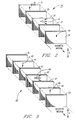
- a preferred embodiment of an MR sensor 30 comprises a first thin film layer 31 of ferromagnetic material, a first thin film layer 33 of a non-magnetic metallic material, a second thin film layer of ferromagnetic material 35, a second thin film layer 37 of a non-magnetic metallic material and a third thin film layer 39 of ferromagnetic material.
- the magnetizations of the two outer layers 31 and 39 of ferromagnetic material are oriented parallel to each other, i.e., in the same direction, and at an angle of about 90 degrees with respect to the magnetization of the intermediate layer 35 of ferromagnetic material in the absence of an externally applied magnetic field as indicated by arrows 32, 34 and 38, respectively.
- the magnetization directions of the first and third outer layers, 31 and 39 of ferromagnetic material are fixed or pinned in a preferred orientation as shown by the arrows 32 and 38.
- the magnetization in the intermediate layer 35 of ferromagnetic material is free to rotate its direction in response to an externally applied magnetic field (such as magnetic field h as shown in Fig. 2), as shown by the dashed arrows 34 on layer 35 in Fig. 2.
- an externally applied magnetic field such as magnetic field h as shown in Fig. 2
- the ferromagnetic layers 31, 35 and 39 can be fabricated of any suitable magnetic material such as cobalt (Co), iron (Fe), nickel (Ni) and their alloys such as nickel-iron (NiFe), nickel-cobalt (NiCo) and iron-cobalt (FeCo), for example.
- the non-magnetic metallic spacer layers 33 and 37 comprise copper (Cu), for example, or other suitable noble metal such as silver (Ag) or gold (Au) or their alloys.
- the fixed or pinned outer ferromagnetic layers 31 and 39 can be exchange biased by adjacent layers (as shown in Fig. 9) of an antiferromagnetic material such as iron-manganese (FeMn), for example.
- an MR sensor based on the spin valve effect wherein a pinned ferromagnetic layer is exchanged biased by an adjacent antiferromagnetic layer is described in greater detail in the above referenced European patent application 93306379.4.
- the magnetization directions of the pinned ferromagnetic layers 31, 39 can be fixed by use of an adjacent hard magnetic layer or by use of a material having a sufficiently high coercivity for the outer pinned layers 31, 39.
- the structure of a conventional or single spin valve MR sensor as described in the above-cited patent applications is essentially FM free /NM/FM pinned /AFM where FM free and FM pinned are ferromagnetic layers separated by a non-magnetic layer NM.
- the orientation of the magnetization of the FM pinned layer is fixed up to some moderate magnetic field by the exchange coupled bias field provided by the antiferromagnetic layer AFM.
- the magnetoresistive effect of the sensor is based on the fact that, when the directions of the magnetization in the adjacent FM layers are different, conduction electrons traversing the NM layer from one FM layer to the other are scattered depending on their spins such that the resistance of the sensor increases.
- This change in resistance is a function of the cosine of the angle between the directions of the magnetizations in the FM layers and is minimum when the magnetizations are parallel, i.e., in the same direction, and maximum when the magnetizations in the layers antiparallel, i.e., in opposite directions.
- the structure described above with reference to Fig. 2 comprises a "dual" spin valve wherein the spin valve structure is doubled symmetrically with respect to the FM free layer.
- the structure of a dual spin valve is AFM 1 /FM p1 /NM 1 /FM free /NM 2 /FM p2 /AFM 2 providing two pairs of FM layers separated by a NM layer which allows utilization of the conduction electrons scattered in both directions from the intermediate FM free layer.
- the directions of magnetization in the two pinned outer layers, FM p1 and FM p2 are fixed by adjacent antiferromagnetic layers AFM 1 and AFM 2 , respectively, while the direction of magnetization in the FM free layer is allowed to rotate freely in response to an applied free magnetic field.
- a dual spin valve sensor comprises the structure FM 1 /S 1 /FM 2 /S 2 /FM 3 as shown.
- the first ferromagnetic layer FM 1 comprises a layer of a first ferromagnetic material 311, such as NiFe, for example, and a thin layer 313, referred to as a "nanolayer", of a second ferromagnetic material, such as Co, for example.
- the nanolayer 313 of the second ferromagnetic material is deposited at the interface between the first ferromagnetic layer and the first spacer layer 371.
- the first ferromagnetic layer forms a bilayer 311, 313 of two different ferromagnetic materials.
- the third ferromagnetic layer FM 3 comprises a bilayer 301, 303 of two different ferromagnetic materials with the nanolayer 303 formed at the interface between the third ferromagnetic layer FM 3 and the second spacer layer 331.
- the second ferromagnetic layer FM 2 Since the second, central ferromagnetic layer FM 2 forms an interface with both spacer layers 331 and 371, the second ferromagnetic layer FM 2 will comprise a trilayer having a centre layer 305 of ferromagnetic material, such as NiFe, for example, with a nanolayer 309, 307 of a second ferromagnetic material, such as Co, for example, formed at the interface with each of the adjacent spacer layers 371, 331, respectively.
- the thickness of the nanolayers is in the range of 0.05 to 2 nm (0.5 to 20 Angstroms).
- the nanolayer can be formed within the ferromagnetic layer at a distance X from the interface between the ferromagnetic layer and the spacer layer.
- the material utilized for the nanolayer can be a non-magnetic material, such as Cr, for example, as well as a ferromagnetic material.
- Magnetoresistive sensors employing nanolayers as described above are described in greater detail in EP-A-529959 (published 3/3/93)
- the thickness of the layers is optimized to provide the highest value of magnetoresistance obtainable for these materials in this structure.
- a preferred embodiment of the dual spin valve formed on a Si substrate having the structure Si/50Ta/20NiFe/110FeMn/60NiFe/25Cu/100NiFe/25Cu/60NiFe/ 110FeMn/50Ta provides a magnetoresistance of 5.5 percent, a 35 percent increase over that obtained from the single spin valve structure.
- the first NiFe layer in the above dual spin valve structure provides a seed layer utilized to obtain the necessary crystalline structure to provide antiferromagnetic FeMn; any material having sufficiently high resistivity to minimize current shunting and which permits the growth of an antiferromagnetic form of FeMn is suitable for use as the seed layer.
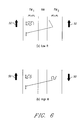
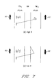
- a dual spin valve MR sensor can be designed wherein the directions of the magnetizations in the outer, pinned ferromagnetic layers are maintained antiparallel to each other, ie, in opposite directions. Further, by proper choice of materials for the different layers, both positive and negative spin-dependent magnetoresistance, referred to as giant magnetoresistance (GMR), can be utilized to produce a high value of (delta R)/R for the sensor. As shown in Fig.
- GMR giant magnetoresistance
- a single spin valve structure having positive GMR comprises two ferromagnetic layers, FM 1 and FM 2 , separated by a nonmagnetic layer, NM, wherein for both ferromagnetic layers the resistivities for spin-up (rho up ) and spin-down (rho down ) satisfy either the relation rho up >rho down or the relation rho up ⁇ rho down .
- the resistance is minimum when the magnetizations, as indicated by arrows 50, of the layers FM 1 and FM 2 are parallel and maximum when the magnetizations of the layers FM 1 and FM 2 are antiparallel. As shown in Fig.
- a single spin valve structure having negative GMR comprises two ferromagnetic layers separated by a nonmagnetic layer wherein for the first ferromagnetic layer, FM 1 , rho up >rho down and for the second ferromagnetic layer, FM 2 , rho up ⁇ rho down .
- the resistance is minimum for antiparallel alignment of the magnetizations, as indicated by arrows 60, and maximum for parallel alignment of the magnetizations.
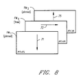
- Fig. 8 illustrates three ferromagnetic layers according to the present invention.
- the GMR is positive producing minimum resistance for parallel alignment of their magnetizations, arrows 71 and 73, respectively.
- the GMR is positive so that minimum resistance is produced for antiparallel alignment of their magnetizations, arrows 73 and 75, respectively.
- the net effect for the structure is that the resistance is maximum when the magnetization of the free layer FM 2 , arrow 73, is aligned parallel with the magnetization of pinned layer FM 3 , arrow 75, and minimum when the magnetization of FM 2 is aligned parallel with the magnetization of pinned layer FM 1 , arrow 71. Additionally, since the magnetizations of the two pinned layers, FM 1 and FM 2 , are aligned in opposite directions, each layer acts as a magnetic flux-keeper for the other layer, thus reducing the demagnetizing effect of the pinned layers.
- an MR sensor 40 comprises a first thin film layer 51 of antiferromagnetic material, a first thin film layer 41 of ferromagnetic material, a first thin film layer 43 of a non-magnetic metallic material, a second thin film layer 45 of ferromagnetic material, a second thin film layer 47 of a non-magnetic metallic material, a third thin film layer 49 of ferromagnetic material and a second thin film layer 53 of antiferromagnetic material.
- the two antiferromagnetic layers 51 and 53 provide a bias field in the adjacent ferromagnetic layers 41 and 49, respectively, by exchange coupling, as is known in the art.
- the magnetizations, as indicated by arrows 42 and 48, respectively, of the two outer ferromagnetic layers 41 and 49 are oriented antiparallel to each other, i.e., in opposite directions, and at an angle of about 90 degrees with respect to the magnetization, as indicated by arrow 44, of the intermediate layer 45 of ferromagnetic material in the absence of an externally applied magnetic field.
- the magnetization direction of the first and third outer layers, 41 and 49 of ferromagnetic material are fixed or pinned in the preferred orientation as shown by the arrows 42 and 48 by the exchange bias of the antiferromagnetic layers 51 and 53, respectively.
- exchange bias layers 51 and 53 comprise different antiferromagnetic materials, preferably FeMn and nickel-manganese (NiMn), respectively, for example.
- the two antiferromagnetic materials have different blocking temperatures, thus allowing the exchange bias direction of each antiferromagnetic layer 51, 53 to be set independent of the other.
- the blocking temperature for the FeMn is approximately 220 degrees C while the blocking temperature for NiMn is much higher.
- the exchange bias direction for the NiMn layer is first set at a relatively high temperature, about 260 degrees C, for example, then the exchange bias direction for the FeMn layer is set a lower temperature, just slightly above the blocking temperature for FeMn, about 230 degrees C, for example.
- a seed layer can be used to insure that the antiferromagnetic layers 51, 53 have the desired structure.
- the materials for the ferromagnetic layers 41, 45 and 49 are chosen to utilize both positive and negative GMR layer pairs. As described above with reference to Fig. 7, materials are chosen such that between the first and second ferromagnetic layers 41 and 45 the GMR is positive, and that between the second and third ferromagnetic layers 45 and 49 the GMR is negative.
- Dilute alloys of vanadium (V) or chromium (Cr) in a Ni or Fe matrix provide ferromagnetic materials wherein rho up >rho down
- Fe or Co in a Ni matrix provide ferromagnetic materials wherein rho up ⁇ rho down , for example.
- Spin-dependent resistivities for Fe or Co diluted with aluminum (Al), iridium (Ir) or Mn are also known.
- the non-magnetic spacer layers 43 and 47 can be any suitable non-magnetic metallic material such as Cu, Au or Ag, for example.
- a suitable underlayer 57 such as Ta, Ru or CrV, for example, is deposited on substrate 55 prior to the deposition of a first antiferromagnetic exchange bias layer 59.
- the purpose of underlayer 57 is to optimize the texture, grain size and morphology of the subsequent layers.
- the morphology can be crucial in obtaining the large MR effects characteristic of dual spin valve structures since it permits the use of very thin non-magnetic metallic spacer layers 63 and 65 between the ferromagnetic layers 61, 65 and 69.
- the underlayer must also have a high resistivity to minimize electrical current shunting effects.
- the underlayer 57 can be omitted.
- Any suitable antiferromagnetic magnetic material may be utilized for the exchange bias layer 59 such as FeMn or NiMn, for example.
- FeMn(60/40 by atomic weight) results in a reduction of the coupling field between the following two ferromagnetic layers where the FeMn antiferromagnetic layer is deposited first.
- a seed layer (not shown) may also be required if the material utilized for the first antiferromagnetic layer 59 cannot be directly deposited with the proper crystalline structure.
- a seed layer preferably of NiFe or AuCu, is desirable to ensure that the antiferromagnetic form of FeMn is obtained.
- a first thin film layer 61 of ferromagnetic material, a first thin film layer 63 of a non-magnetic metallic material, a second thin film layer 65 of ferromagnetic material, a second thin film layer 67 of a non-magnetic metallic material, a third thin film layer 69 of ferromagnetic material and a second thin film exchange bias layer 71 of antiferromagnetic material are deposited over underlayer 57.
- the first and third ferromagnetic layers 61 and 69 have their magnetizations oriented parallel to each other and at an angle of approximately 90 degrees with respect to the magnetization of the second, intermediate ferromagnetic layer 65 in the absence of an applied magnetic field.
- the magnetization directions of the first and third ferromagnetic layers 61 and 69 are fixed or pinned in position by a biasing field produced by exchange coupling.
- the outer ferromagnetic layers 61, 69 can be pinned utilizing an adjacent hard magnetic layer or by utilizing materials having relatively high coercivities for the outer ferromagnetic layers and setting the magnetization directions during fabrication. If the magnetization directions of the outer ferromagnetic layers 61, 69 are different, antiparallel, for example, the coercivity for each layer will have to be different to allow the magnetization direction of one layer to be set independent of the other layer.
- the ferromagnetic layers 61, 65 and 69 can be fabricated of any suitable magnetic material such as Co, Fe, Ni and their alloys such as NiFe, NiCo and FeCo, for example.
- the thicknesses of the ferromagnetic layers 61, 65 and 69 can be selected from a range of about 0.5 nm (5 Angstroms) to about 15 nm (150 Angstroms).
- the non-magnetic spacer layers 63 and 67 are preferably metallic with high conductivity. Noble materials such as Au, Ag and Cu provide large MR response, Pt and Pd provide small MR response, while Cr and Ta exhibit very little MR response.
- the thickness of the non-magnetic spacer layers 63 and 67 is less than the mean free path of the conduction electrons in the sensor, preferably within the range of about 1 nm (10 Angstroms) to about 4 nm (40 Angstroms).
- a longitudinal bias field parallel to the longitudinal direction of the magnetic layers in the sensor in order to minimize Barkhausen noise it is desirable to provide a longitudinal bias field parallel to the longitudinal direction of the magnetic layers in the sensor.
- layers 75 of a suitable magnetically hard material are deposited over the end regions of the sensor thus providing a longitudinal bias field in a central active region 78 of the sensor.
- the longitudinal bias field can be provided by exchange coupling with antiferromagnetic layers formed over the sensor end regions in direct contact with the ferromagnetic layers.
Landscapes
- Engineering & Computer Science (AREA)
- Chemical & Material Sciences (AREA)
- Nanotechnology (AREA)
- Crystallography & Structural Chemistry (AREA)
- Manufacturing & Machinery (AREA)
- Physics & Mathematics (AREA)
- Mathematical Physics (AREA)
- Theoretical Computer Science (AREA)
- Magnetic Heads (AREA)
- Hall/Mr Elements (AREA)
Claims (29)
- Capteur magnétorésistif comprenant :
une structure à couches formée sur un substrat, la structure comprenant une première couche (31), une seconde couche (35) et une troisième couche (39) d'un matériau ferromagnétique, chaque couche desdites couches de matériau ferromagnétique étant séparée de la couche adjacente de matériau ferromagnétique par une couche (33, 37) de matériau métallique non magnétique, ladite seconde couche du matériau ferromagnétique étant disposée entre lesdites première et troisième couches d'un matériau ferromagnétique, la direction de la magnétisation étant fixée dans lesdites première et troisième couches du matériau ferromagnétique, la direction de la magnétisation dans ladite seconde couche du matériau ferromagnétique étant pratiquement perpendiculaire auxdites directions fixées de la magnétisation dans lesdites première et troisième couches d'un matériau ferromagnétique à un champ magnétique nul appliqué. - Capteur magnétorésistif selon la revendication 1, dans lequel chaque couche desdites couches de matériau ferromagnétique comprend de plus au moins une couche supplémentaire de matériau.
- Capteur magnétorésistif selon la revendication 2, dans lequel ladite couche supplémentaire de matériau comprend au moins une nanocouche de matériau ferromagnétique.
- Capteur magnétorésistif selon la revendication 3, dans lequel chaque dite couche de matériau ferromagnétique comprend de plus une nanocouche d'un matériau ferromagnétique différent disposée à l'interface entre ladite couche de matériau ferromagnétique et ladite couche de matériau métallique non magnétique.
- Capteur magnétorésistif selon la revendication 4, dans lequel chaque couche desdites première et troisième couches de matériau ferromagnétique forme une bicouche comprenant une couche d'un premier matériau ferromagnétique et une nanocouche d'un second matériau ferromagnétique, ladite nanocouche disposée à l'interface entre lesdites première et troisième couches de matériau ferromagnétique et ladite couche de matériau métallique non magnétique séparant lesdites première et troisième couches de matériau ferromagnétique, respectivement, de ladite seconde couche de matériau ferromagnétique, et ladite seconde couche de matériau ferromagnétique formant une tricouche comprenant une couche d'un premier matériau ferromagnétique et deux nanocouches d'un second matériau ferromagnétique, lesdites nanocouches disposées aux interfaces entre ladite seconde couche de matériau ferromagnétique et lesdites couches de matériau métallique non magnétique séparant ladite seconde couche de matériau ferromagnétique desdites première et troisième couches de matériau ferromagnétique, respectivement.
- Capteur magnétorésistif selon la revendication 3, dans lequel ladite nanocouche présente une épaisseur dans la plage d'environ 0,05 nm (0,5 Angströms) à environ 2 nm (20,0 Angströms).
- Capteur magnétorésistif selon l'une quelconque des revendications précédentes, comprenant de plus un moyen de fixation pour fixer la direction de la magnétisation dans lesdites première et troisième couches du matériau ferromagnétique.
- Capteur magnétorésistif selon la revendication 7, le moyen de fixation comprenant une première couche d'un matériau magnétiquement dur adjacente à ladite première couche de matériau magnétique et une seconde couche d'un matériau magnétiquement dur adjacente à ladite troisième couche de matériau ferromagnétique, lesdites première et seconde couches de matériau magnétiquement dur servant à délivrer un champ de polarisation magnétique dans lesdites première et troisième couches du matériau ferromagnétique, respectivement, fixant de ce fait la direction de la magnétisation dans lesdites couches.
- Capteur magnétorésistif selon la revendication 7, le moyen de fixation comprenant une première couche (52) d'un matériau anti-ferromagnétique adjacente et en contact avec ladite première couche de matériau ferromagnétique et une seconde couche (53) d'un matériau anti-ferromagnétique adjacente et en contact avec ladite troisième couche de matériau ferromagnétique, lesdites première et seconde couches de matériau anti-ferromagnétique servant à délivrer un champ de polarisation magnétique dans lesdites première et troisième couches de matériau ferromagnétique, respectivement, fixant de ce fait la direction de la magnétisation dans lesdites couches.
- Capteur magnétorésistif selon la revendication 9, dans lequel lesdites première et seconde couches du matériau anti-ferromagnétique sont constituées d'un matériau choisi dans le groupe comprenant le fer-manganèse, le nickel-manganèse et le fer-nickel-manganèse.
- Capteur magnétorésistif selon la revendication 10, dans lequel lesdites première et seconde couches de matériau anti-ferromagnétique comprennent du fer-manganèse.
- Capteur magnétorésistif selon l'une quelconque des revendications 9 à 11, dans lequel lesdites première et seconde couches de matériau anti-ferromagnétique ont une épaisseur à l'intérieur de la plage d'environ 5 nm (50 Angströms) à environ 20 nm (200 Angströms).
- Capteur magnétorésistif selon l'une quelconque des revendications précédentes, dans lequel lesdites première, seconde et troisième couches de matériau ferromagnétique sont constituées d'un matériau choisi dans le groupe qui est constitué du fer, du cobalt et du nickel et des alliages de fer, cobalt ou nickel.
- Capteur magnétorésistif selon la revendication 13, dans lequel lesdites première, seconde et troisième couches de matériau ferromagnétique sont constituées d'un alliage de nickel-fer.
- Capteur magnétorésistif selon la revendication 13 ou la revendication 14, dans lequel lesdites première, seconde et troisième couches de matériau ferromagnétique ont une épaisseur à l'intérieur de la plage d'environ 0,5 nm (5 Angströms) à environ 15 nm (150 Angströms).
- Capteur magnétorésistif selon l'une quelconque des revendications précédentes, dans lequel ladite couche de séparation métallique non magnétique a une épaisseur inférieure à la longueur du libre parcours moyen des électrons de conduction dans ladite couche de séparation métallique non magnétique.
- Capteur magnétorésistif selon la revendication 16, dans lequel ladite couche de séparation métallique non magnétique a une épaisseur à l'intérieur de la plage d'environ 1 nm (10 Angströms) à environ 4 nm (40 Angströms).
- Capteur magnétorésistif selon l'une quelconque des revendications précédentes, dans lequel chaque couche de séparation métallique non magnétique est constituée d'un matériau choisi dans le groupe comprenant l'argent, l'or, le cuivre et des alliages d'argent, de cuivre et d'or.
- Capteur magnétorésistif selon la revendication 18, dans lequel chaque couche de séparation métallique non magnétique comprend une couche à film mince de cuivre.
- Capteur magnétorésistif selon l'une quelconque des revendications précédentes, dans lequel les directions de la magnétisation dans les première et troisième couches du matériau ferromagnétique sont alignées en une orientation parallèle.
- Capteur magnétorésistif selon l'une quelconque des revendications 1 à 19, dans lequel lesdites première et seconde couches de matériau ferromagnétique forment une première paire de couches ferromagnétiques séparées par une couche non magnétique ayant une magnétorésistance positive importante entre celles-ci et lesdites seconde et troisième couches de matériau ferromagnétique forment une seconde paire de couches ferromagnétiques séparées par une couche non magnétique ayant une magnétorésistance négative importante entre celles-ci.
- Capteur magnétorésistif selon la revendication 21, dans lequel les directions de la magnétisation dans les première et troisième couches du matériau ferromagnétique sont alignées en une orientation antiparallèle.
- Capteur magnétorésistif selon la revendication 20 ou la revendication 21, comprenant de plus une couche d'un premier matériau anti-ferromagnétique adjacente et en contact avec ladite première couche de matériau ferromagnétique et une couche d'un second matériau anti-ferromagnétique adjacente et en contact avec ladite troisième couche de matériau ferromagnétique, lesdites première et seconde couches de matériau anti-ferromagnétique servant à délivrer un champ de polarisation magnétique dans lesdites première et troisième couches du matériau ferromagnétique, respectivement, fixant de ce fait la direction de la magnétisation dans lesdites couches.
- Capteur magnétorésistif selon la revendication 23, dans lequel lesdits premier et second matériaux anti-ferromagnétiques ont des températures de blocage différentes.
- Capteur magnétorésistif selon la revendication 23 ou la revendication 24, dans lequel chacune desdites première et troisième couches du matériau ferromagnétique comprend un matériau ferromagnétique ayant une coercivité différente que la coercivité du matériau ferromagnétique de l'autre couche.
- Système de stockage magnétique comprenant :un support de stockage magnétique ayant une pluralité de pistes pour l'enregistrement des données ;un transducteur magnétique maintenu en position très proche par rapport audit support de stockage magnétique pendant le déplacement relatif entre ledit transducteur magnétique et ledit support de stockage magnétique, ledit transducteur magnétique comprenant un capteur de lecture magnétorésistif selon l'une quelconque des revendications précédentes ;un moyen d'organe d'actionnement couplé audit transducteur magnétique pour déplacer ledit transducteur magnétique sur les pistes sélectionnées sur le support de stockage magnétique ; etun moyen de détection couplé audit capteur de lecture magnétorésistif pour détecter les changements de valeur ohmique dans ledit matériau magnétorésistif en réponse au champ magnétique représentatif desdites informations enregistrées dans ledit support de stockage magnétique intercepté par ledit capteur magnétorésistif.
- Système de stockage magnétique selon la revendication 26, dans lequel ledit capteur magnétorésistif comprend de plus :une couche de protection déposée sur ladite seconde couche anti-ferromagnétique ; etun moyen de conducteur électrique déposé sur ladite couche de protection pour coupler ledit capteur magnétorésistif audit moyen de détection.
- Système de stockage magnétique selon la revendication 27, dans lequel ladite couche de protection comprend un matériau choisi dans le groupe comprenant le tantale et le zirconium.
- Système de stockage magnétique selon la revendication 27 ou la revendication 28, comprenant de plus un moyen pour délivrer un champ de polarisation longitudinale dans une partie active dudit capteur magnétorésistif.
Applications Claiming Priority (2)
| Application Number | Priority Date | Filing Date | Title |
|---|---|---|---|
| US973106 | 1992-11-06 | ||
| US07/973,106 US5287238A (en) | 1992-11-06 | 1992-11-06 | Dual spin valve magnetoresistive sensor |
Publications (3)
| Publication Number | Publication Date |
|---|---|
| EP0596689A2 EP0596689A2 (fr) | 1994-05-11 |
| EP0596689A3 EP0596689A3 (fr) | 1995-02-08 |
| EP0596689B1 true EP0596689B1 (fr) | 1998-01-28 |
Family
ID=25520504
Family Applications (1)
| Application Number | Title | Priority Date | Filing Date |
|---|---|---|---|
| EP93308726A Expired - Lifetime EP0596689B1 (fr) | 1992-11-06 | 1993-11-01 | Capteur magnétorésistif |
Country Status (5)
| Country | Link |
|---|---|
| US (1) | US5287238A (fr) |
| EP (1) | EP0596689B1 (fr) |
| JP (1) | JP2592216B2 (fr) |
| DE (1) | DE69316708T2 (fr) |
| SG (1) | SG42845A1 (fr) |
Cited By (1)
| Publication number | Priority date | Publication date | Assignee | Title |
|---|---|---|---|---|
| US6245450B1 (en) | 1997-11-17 | 2001-06-12 | Matsushita Electric Industrial Co., Ltd. | Exchange coupling film magnetoresistance effect device magnetoresistance effective head and method for producing magnetoresistance effect device |
Families Citing this family (166)
| Publication number | Priority date | Publication date | Assignee | Title |
|---|---|---|---|---|
| US5633092A (en) * | 1991-12-10 | 1997-05-27 | British Technology Group Ltd. | Magnetostrictive material |
| JP3022023B2 (ja) | 1992-04-13 | 2000-03-15 | 株式会社日立製作所 | 磁気記録再生装置 |
| SG47479A1 (en) * | 1992-08-25 | 1998-04-17 | Seagate Technology | A magnetoresistive sensor and method of making the same |
| US5617071A (en) * | 1992-11-16 | 1997-04-01 | Nonvolatile Electronics, Incorporated | Magnetoresistive structure comprising ferromagnetic thin films and intermediate alloy layer having magnetic concentrator and shielding permeable masses |
| US5569544A (en) * | 1992-11-16 | 1996-10-29 | Nonvolatile Electronics, Incorporated | Magnetoresistive structure comprising ferromagnetic thin films and intermediate layers of less than 30 angstroms formed of alloys having immiscible components |
| JPH08503336A (ja) * | 1992-11-16 | 1996-04-09 | ノンボラタイル エレクトロニクス,インコーポレイテッド | 合金層を有する磁気抵抗性構造 |
| KR100225179B1 (ko) * | 1992-11-30 | 1999-10-15 | 니시무로 타이죠 | 박막 자기 헤드 및 자기 저항 효과형 헤드 |
| DE4243358A1 (de) * | 1992-12-21 | 1994-06-23 | Siemens Ag | Magnetowiderstands-Sensor mit künstlichem Antiferromagneten und Verfahren zu seiner Herstellung |
| DE4243357A1 (de) * | 1992-12-21 | 1994-06-23 | Siemens Ag | Magnetowiderstands-Sensor mit verkürzten Meßschichten |
| DE4301704A1 (de) * | 1993-01-22 | 1994-07-28 | Siemens Ag | Vorrichtung zum Erfassen einer Winkelposition eines Objektes |
| JP3219329B2 (ja) * | 1993-02-03 | 2001-10-15 | 財団法人生産開発科学研究所 | 磁気抵抗効果素子 |
| US5422571A (en) * | 1993-02-08 | 1995-06-06 | International Business Machines Corporation | Magnetoresistive spin valve sensor having a nonmagnetic back layer |
| FR2702919B1 (fr) * | 1993-03-19 | 1995-05-12 | Thomson Csf | Transducteur magnétorésistif et procédé de réalisation. |
| JP2784457B2 (ja) * | 1993-06-11 | 1998-08-06 | インターナショナル・ビジネス・マシーンズ・コーポレイション | 磁気抵抗センサ装置 |
| JPH0766033A (ja) * | 1993-08-30 | 1995-03-10 | Mitsubishi Electric Corp | 磁気抵抗素子ならびにその磁気抵抗素子を用いた磁性薄膜メモリおよび磁気抵抗センサ |
| US5585199A (en) * | 1993-09-09 | 1996-12-17 | Kabushiki Kaisha Toshiba | Magnetoresistance effect head |
| JP2860233B2 (ja) * | 1993-09-09 | 1999-02-24 | 株式会社日立製作所 | 巨大磁気抵抗効果型磁気ヘッドおよびそれを用いた磁気記録再生装置 |
| US5475304A (en) * | 1993-10-01 | 1995-12-12 | The United States Of America As Represented By The Secretary Of The Navy | Magnetoresistive linear displacement sensor, angular displacement sensor, and variable resistor using a moving domain wall |
| SG55066A1 (en) * | 1993-10-06 | 1999-06-22 | Koninkl Philips Electronics Nv | Magneto-resistance device and magnetic head employing such a device |
| US5408377A (en) * | 1993-10-15 | 1995-04-18 | International Business Machines Corporation | Magnetoresistive sensor with improved ferromagnetic sensing layer and magnetic recording system using the sensor |
| US5465185A (en) * | 1993-10-15 | 1995-11-07 | International Business Machines Corporation | Magnetoresistive spin valve sensor with improved pinned ferromagnetic layer and magnetic recording system using the sensor |
| US5549977A (en) * | 1993-11-18 | 1996-08-27 | Lucent Technologies Inc. | Article comprising magnetoresistive material |
| US6002553A (en) * | 1994-02-28 | 1999-12-14 | The United States Of America As Represented By The United States Department Of Energy | Giant magnetoresistive sensor |
| DE69511145T2 (de) * | 1994-03-09 | 2000-02-03 | Eastman Kodak Co., Rochester | Magnetoresistiver Wiedergabekopf mit doppeltem Spin-Ventilelement |
| CN1095153C (zh) * | 1994-03-10 | 2002-11-27 | 国际商业机器公司 | 磁电阻传感元件及磁电阻传感器 |
| US5828525A (en) * | 1994-03-15 | 1998-10-27 | Kabushiki Kaisha Toshiba | Differential detection magnetoresistance head |
| US5712751A (en) * | 1994-03-17 | 1998-01-27 | Kabushiki Kaisha Toshiba | Magnetic sensor and magnetic recording-reproducing head and magnetic recording-reproducing apparatus using same |
| EP0677750A3 (fr) * | 1994-04-15 | 1996-04-24 | Hewlett Packard Co | Capteur magnétorésistif géant avec une couche d'ancrage. |
| US5841611A (en) * | 1994-05-02 | 1998-11-24 | Matsushita Electric Industrial Co., Ltd. | Magnetoresistance effect device and magnetoresistance effect type head, memory device, and amplifying device using the same |
| US6256222B1 (en) | 1994-05-02 | 2001-07-03 | Matsushita Electric Industrial Co., Ltd. | Magnetoresistance effect device, and magnetoresistaance effect type head, memory device, and amplifying device using the same |
| US5546253A (en) * | 1994-05-06 | 1996-08-13 | Quantum Corporation | Digitial output magnetoresistive (DOMR) head and methods associated therewith |
| US5442508A (en) * | 1994-05-25 | 1995-08-15 | Eastman Kodak Company | Giant magnetoresistive reproduce head having dual magnetoresistive sensor |
| US5583725A (en) * | 1994-06-15 | 1996-12-10 | International Business Machines Corporation | Spin valve magnetoresistive sensor with self-pinned laminated layer and magnetic recording system using the sensor |
| US5528440A (en) * | 1994-07-26 | 1996-06-18 | International Business Machines Corporation | Spin valve magnetoresistive element with longitudinal exchange biasing of end regions abutting the free layer, and magnetic recording system using the element |
| US5898546A (en) * | 1994-09-08 | 1999-04-27 | Fujitsu Limited | Magnetoresistive head and magnetic recording apparatus |
| JPH0877519A (ja) * | 1994-09-08 | 1996-03-22 | Fujitsu Ltd | 磁気抵抗効果型トランスジューサ |
| FR2724481B1 (fr) * | 1994-09-13 | 1996-10-18 | Commissariat Energie Atomique | Tete magnetique planaire a magnetoresistance multicouche longitudinale |
| US5991125A (en) * | 1994-09-16 | 1999-11-23 | Kabushiki Kaisha Toshiba | Magnetic head |
| US5434826A (en) * | 1994-09-26 | 1995-07-18 | Read-Rite Corporation | Multilayer hard bias films for longitudinal biasing in magnetoresistive transducer |
| US5561368A (en) * | 1994-11-04 | 1996-10-01 | International Business Machines Corporation | Bridge circuit magnetic field sensor having spin valve magnetoresistive elements formed on common substrate |
| US5896251A (en) * | 1994-12-26 | 1999-04-20 | Kabushiki Kaisha Toshiba | Magnetoresistance effect head with conductor film pair and magnetic field proving film pair disposed between substrate and magnetoresistance effect film |
| US5515221A (en) * | 1994-12-30 | 1996-05-07 | International Business Machines Corporation | Magnetically stable shields for MR head |
| US5664316A (en) * | 1995-01-17 | 1997-09-09 | International Business Machines Corporation | Method of manufacturing magnetoresistive read transducer having a contiguous longitudinal bias layer |
| FR2729790A1 (fr) * | 1995-01-24 | 1996-07-26 | Commissariat Energie Atomique | Magnetoresistance geante, procede de fabrication et application a un capteur magnetique |
| DE19507303A1 (de) * | 1995-03-02 | 1996-09-05 | Siemens Ag | Sensoreinrichtung mit einer Brückenschaltung von magnetoresistiven Sensorelementen |
| US5608593A (en) * | 1995-03-09 | 1997-03-04 | Quantum Peripherals Colorado, Inc. | Shaped spin valve type magnetoresistive transducer and method for fabricating the same incorporating domain stabilization technique |
| JP3629309B2 (ja) * | 1995-09-05 | 2005-03-16 | アルプス電気株式会社 | 薄膜磁気ヘッド |
| EP0749112B1 (fr) * | 1995-06-15 | 2002-02-13 | TDK Corporation | Transducteur magnétorésistif à structure "spin-valve" et procédé de fabrication |
| JP3651619B2 (ja) * | 1995-06-29 | 2005-05-25 | 富士通株式会社 | 磁気抵抗効果型トランスデューサ及び磁気記録装置 |
| SG46731A1 (en) * | 1995-06-30 | 1998-02-20 | Ibm | Spin valve magnetoresistive sensor with antiparallel pinned layer and improved exchange bias layer and magnetic recording system using the senor |
| JP2849354B2 (ja) * | 1995-07-28 | 1999-01-20 | ティーディーケイ株式会社 | 磁気変換素子及び薄膜磁気ヘッド |
| US5896252A (en) * | 1995-08-11 | 1999-04-20 | Fujitsu Limited | Multilayer spin valve magneto-resistive effect magnetic head with free magnetic layer including two sublayers and magnetic disk drive including same |
| US5648885A (en) * | 1995-08-31 | 1997-07-15 | Hitachi, Ltd. | Giant magnetoresistive effect sensor, particularly having a multilayered magnetic thin film layer |
| US5701222A (en) * | 1995-09-11 | 1997-12-23 | International Business Machines Corporation | Spin valve sensor with antiparallel magnetization of pinned layers |
| JPH0983039A (ja) * | 1995-09-14 | 1997-03-28 | Nec Corp | 磁気抵抗効果素子 |
| US5768067A (en) | 1995-09-19 | 1998-06-16 | Alps Electric Co., Ltd. | Magnetoresistive head using exchange anisotropic magnetic field with an antiferromagnetic layer |
| US5923504A (en) * | 1995-09-21 | 1999-07-13 | Tdk Corporation | Magnetoresistance device |
| KR100201681B1 (ko) * | 1996-01-03 | 1999-06-15 | 포만 제프리 엘 | 직교 자기저항 센서와 자기 저장 시스템 및 직교 자기저항 센서 제조 방법 |
| US6124711A (en) * | 1996-01-19 | 2000-09-26 | Fujitsu Limited | Magnetic sensor using tunnel resistance to detect an external magnetic field |
| EP0789250A3 (fr) * | 1996-02-12 | 1997-10-01 | Read Rite Corp | Transducteur magnétorésistif géant à couche mince muni d'un structure de guide de flux |
| JPH09274710A (ja) * | 1996-04-04 | 1997-10-21 | Fujitsu Ltd | スピンバルブ磁気抵抗効果ヘッドとその製造方法及び磁気記録装置 |
| KR100262282B1 (ko) * | 1996-04-30 | 2000-10-02 | 니시무로 타이죠 | 자기 저항 효과 소자 |
| US5744950A (en) * | 1996-05-09 | 1998-04-28 | Ssi Technologies, Inc. | Apparatus for detecting the speed of a rotating element including signal conditioning to provide a fifty percent duty cycle |
| US5668688A (en) * | 1996-05-24 | 1997-09-16 | Quantum Peripherals Colorado, Inc. | Current perpendicular-to-the-plane spin valve type magnetoresistive transducer |
| US5742162A (en) * | 1996-07-17 | 1998-04-21 | Read-Rite Corporation | Magnetoresistive spin valve sensor with multilayered keeper |
| FR2752302B1 (fr) * | 1996-08-08 | 1998-09-11 | Commissariat Energie Atomique | Capteur de champ magnetique a pont de magnetoresistances |
| US5793279A (en) * | 1996-08-26 | 1998-08-11 | Read-Rite Corporation | Methods and compositions for optimizing interfacial properties of magnetoresistive sensors |
| US5705973A (en) * | 1996-08-26 | 1998-01-06 | Read-Rite Corporation | Bias-free symmetric dual spin valve giant magnetoresistance transducer |
| US5945904A (en) * | 1996-09-06 | 1999-08-31 | Ford Motor Company | Giant magnetoresistors with high sensitivity and reduced hysteresis and thin layers |
| US5696656A (en) * | 1996-09-06 | 1997-12-09 | International Business Machines Corporation | Highly sensitive orthogonal spin valve read head |
| US5869963A (en) | 1996-09-12 | 1999-02-09 | Alps Electric Co., Ltd. | Magnetoresistive sensor and head |
| US6249406B1 (en) * | 1996-09-23 | 2001-06-19 | International Business Machines Corporation | Magnetoresistive sensor with a soft adjacent layer having high magnetization, high resistivity, low intrinsic anisotropy and near zero magnetostriction |
| JP3291208B2 (ja) | 1996-10-07 | 2002-06-10 | アルプス電気株式会社 | 磁気抵抗効果型センサおよびその製造方法とそのセンサを備えた磁気ヘッド |
| US5717550A (en) * | 1996-11-01 | 1998-02-10 | Read-Rite Corporation | Antiferromagnetic exchange biasing using buffer layer |
| US5796561A (en) * | 1996-11-27 | 1998-08-18 | International Business Machines Corporation | Self-biased spin valve sensor |
| US5768069A (en) * | 1996-11-27 | 1998-06-16 | International Business Machines Corporation | Self-biased dual spin valve sensor |
| JPH10162322A (ja) | 1996-11-28 | 1998-06-19 | Nec Corp | 磁気抵抗効果型複合ヘッドおよびその製造方法 |
| US6535362B2 (en) * | 1996-11-28 | 2003-03-18 | Matsushita Electric Industrial Co., Ltd. | Magnetoresistive device having a highly smooth metal reflective layer |
| JP3886589B2 (ja) * | 1997-03-07 | 2007-02-28 | アルプス電気株式会社 | 巨大磁気抵抗効果素子センサ |
| JP3255872B2 (ja) | 1997-04-17 | 2002-02-12 | アルプス電気株式会社 | スピンバルブ型薄膜素子及びその製造方法 |
| US5818685A (en) * | 1997-05-05 | 1998-10-06 | Read-Rite Corporation | CIP GMR sensor coupled to biasing magnet with spacer therebetween |
| US5748399A (en) * | 1997-05-13 | 1998-05-05 | International Business Machines Corporation | Resettable symmetric spin valve |
| US6118622A (en) * | 1997-05-13 | 2000-09-12 | International Business Machines Corporation | Technique for robust resetting of spin valve head |
| US5825595A (en) * | 1997-05-13 | 1998-10-20 | International Business Machines Corporation | Spin valve sensor with two spun values separated by an insulated current conductor |
| JP2985964B2 (ja) * | 1997-06-30 | 1999-12-06 | 日本電気株式会社 | 磁気抵抗効果型ヘッド及びその初期化方法 |
| US6222702B1 (en) | 1997-08-15 | 2001-04-24 | Seagate Technology, Inc. | Magnetic read element shield having dimensions that minimize domain wall movement |
| US5856617A (en) * | 1997-09-02 | 1999-01-05 | International Business Machines Corporation | Atomic force microscope system with cantilever having unbiased spin valve magnetoresistive strain gauge |
| US6350487B1 (en) | 1997-09-24 | 2002-02-26 | Alps Electric Co., Ltd. | Spin-valve type thin film element and its manufacturing method |
| JP3227116B2 (ja) * | 1997-09-24 | 2001-11-12 | アルプス電気株式会社 | スピンバルブ型薄膜素子およびその製造方法 |
| JP3833362B2 (ja) * | 1997-10-01 | 2006-10-11 | 富士通株式会社 | 磁気抵抗効果型ヘッド |
| JP3263016B2 (ja) * | 1997-10-20 | 2002-03-04 | アルプス電気株式会社 | スピンバルブ型薄膜素子 |
| JP3175922B2 (ja) * | 1997-10-24 | 2001-06-11 | アルプス電気株式会社 | スピンバルブ型薄膜素子の製造方法 |
| EP0917161B1 (fr) * | 1997-11-17 | 2003-02-19 | Matsushita Electronics Corporation | Film mince à accouplement d'interchange, élément magnétorésistif, tête magnétorésistive et procédé de fabrication |
| JP3269999B2 (ja) * | 1997-12-09 | 2002-04-02 | アルプス電気株式会社 | 薄膜磁気ヘッドの製造方法 |
| US6074767A (en) * | 1998-03-12 | 2000-06-13 | International Business Machines Corporation | Spin valve magnetoresistive head with two sets of ferromagnetic/antiferromagnetic films having high blocking temperatures and fabrication method |
| JP3790356B2 (ja) * | 1998-03-19 | 2006-06-28 | 富士通株式会社 | Gmrヘッド、gmrヘッドの製造方法及び磁気ディスク駆動装置 |
| US6639764B2 (en) | 1998-07-21 | 2003-10-28 | Alps Electric Co., Ltd. | Spin-valve magnetoresistive thin film element |
| JP2000040212A (ja) | 1998-07-24 | 2000-02-08 | Alps Electric Co Ltd | スピンバルブ型薄膜素子 |
| JP2000057527A (ja) | 1998-08-04 | 2000-02-25 | Alps Electric Co Ltd | スピンバルブ型薄膜素子 |
| US6215695B1 (en) * | 1998-12-08 | 2001-04-10 | Canon Kabushiki Kaisha | Magnetoresistance element and magnetic memory device employing the same |
| US6587315B1 (en) | 1999-01-20 | 2003-07-01 | Alps Electric Co., Ltd. | Magnetoresistive-effect device with a magnetic coupling junction |
| US6277505B1 (en) | 1999-01-21 | 2001-08-21 | Read-Rite Corporation | Read sensor with improved thermal stability and manufacturing method therefor |
| US6418000B1 (en) | 1999-01-21 | 2002-07-09 | Read-Rite Corporation | Dual, synthetic spin valve sensor using current pinning |
| JP3703348B2 (ja) | 1999-01-27 | 2005-10-05 | アルプス電気株式会社 | スピンバルブ型薄膜素子とそのスピンバルブ型薄膜素子を備えた薄膜磁気ヘッド |
| JP3212567B2 (ja) * | 1999-01-27 | 2001-09-25 | アルプス電気株式会社 | 磁気抵抗効果型薄膜磁気素子を備えた薄膜磁気ヘッドおよびその製造方法 |
| JP3212569B2 (ja) | 1999-01-27 | 2001-09-25 | アルプス電気株式会社 | デュアルスピンバルブ型薄膜磁気素子及び薄膜磁気ヘッド及びデュアルスピンバルブ型薄膜磁気素子の製造方法 |
| US6181533B1 (en) | 1999-02-19 | 2001-01-30 | Seagate Technology Llc | Simultaneous fixation of the magnetization direction in a dual GMR sensor's pinned layers |
| US6583971B1 (en) * | 1999-03-09 | 2003-06-24 | Sae Magnetics (Hk) Ltd. | Elimination of electric-pop noise in MR/GMR device |
| US6331773B1 (en) | 1999-04-16 | 2001-12-18 | Storage Technology Corporation | Pinned synthetic anti-ferromagnet with oxidation protection layer |
| JP2000331316A (ja) * | 1999-05-20 | 2000-11-30 | Tdk Corp | 磁気抵抗効果型ヘッド |
| JP2000348310A (ja) * | 1999-06-03 | 2000-12-15 | Alps Electric Co Ltd | スピンバルブ型薄膜素子およびそのスピンバルブ型薄膜素子を備えた薄膜磁気ヘッド |
| US6219208B1 (en) * | 1999-06-25 | 2001-04-17 | International Business Machines Corporation | Dual spin valve sensor with self-pinned layer specular reflector |
| US6317298B1 (en) * | 1999-06-25 | 2001-11-13 | International Business Machines Corporation | Spin valve read sensor with specular reflector structure between a free layer structure and a keeper layer |
| US6366420B1 (en) | 1999-07-13 | 2002-04-02 | Texas Instruments Incorporated | Method of restoring the orientation of a pinned layer of a magnetoresistive head |
| US6449134B1 (en) * | 1999-08-05 | 2002-09-10 | International Business Machines Corporation | Read head with file resettable dual spin valve sensor |
| US6611405B1 (en) * | 1999-09-16 | 2003-08-26 | Kabushiki Kaisha Toshiba | Magnetoresistive element and magnetic memory device |
| US6326637B1 (en) | 1999-10-18 | 2001-12-04 | International Business Machines Corporation | Antiferromagnetically exchange-coupled structure for magnetic tunnel junction device |
| US6381105B1 (en) | 1999-10-22 | 2002-04-30 | Read-Rite Corporation | Hybrid dual spin valve sensor and method for making same |
| US6411476B1 (en) * | 1999-10-28 | 2002-06-25 | International Business Machines Corporation | Trilayer seed layer structure for spin valve sensor |
| US6447935B1 (en) | 1999-11-23 | 2002-09-10 | Read-Rite Corporation | Method and system for reducing assymetry in a spin valve having a synthetic pinned layer |
| US6430013B1 (en) | 1999-12-06 | 2002-08-06 | International Business Machines Corporation | Magnetoresistive structure having improved thermal stability via magnetic barrier layer within a free layer |
| US6519117B1 (en) | 1999-12-06 | 2003-02-11 | International Business Machines Corporation | Dual AP pinned GMR head with offset layer |
| US6643103B1 (en) * | 2000-01-05 | 2003-11-04 | Seagate Technology Llc | Very high linear resolution CPP differential dual spin valve magnetoresistive head |
| US20010030839A1 (en) * | 2000-01-13 | 2001-10-18 | Lieping Zhong | Dual spin-valve magnetoresistive sensor |
| US20010045826A1 (en) * | 2000-03-16 | 2001-11-29 | Schneider Mark R. | Distortion immune magnetic field generator for magnetic tracking systems and method of generating magnetic fields |
| JP4136261B2 (ja) * | 2000-03-29 | 2008-08-20 | 富士通株式会社 | 磁気抵抗効果素子を製造する方法 |
| US6583969B1 (en) * | 2000-04-12 | 2003-06-24 | International Business Machines Corporation | Pinned layer structure having nickel iron film for reducing coercivity of a free layer structure in a spin valve sensor |
| JP2001307308A (ja) * | 2000-04-24 | 2001-11-02 | Fujitsu Ltd | 磁気抵抗効果型ヘッドおよび情報再生装置 |
| US6473275B1 (en) | 2000-06-06 | 2002-10-29 | International Business Machines Corporation | Dual hybrid magnetic tunnel junction/giant magnetoresistive sensor |
| US6549382B1 (en) | 2000-06-14 | 2003-04-15 | International Business Machines Corporation | Read head with asymmetric dual AP pinned spin valve sensor |
| US6560078B1 (en) | 2000-07-13 | 2003-05-06 | International Business Machines Corporation | Bilayer seed layer for spin valves |
| US6680827B2 (en) | 2000-08-07 | 2004-01-20 | Tdk Corporation | Dual spin valve CPP MR with flux guide between free layers thereof |
| US6853520B2 (en) | 2000-09-05 | 2005-02-08 | Kabushiki Kaisha Toshiba | Magnetoresistance effect element |
| US6580588B1 (en) | 2000-10-06 | 2003-06-17 | International Business Machines Corporation | Resettable dual AP pinned valve sensor insensitive to sense current direction and having symmetrically balanced fields about a free layer |
| US6714389B1 (en) | 2000-11-01 | 2004-03-30 | Seagate Technology Llc | Digital magnetoresistive sensor with bias |
| US6624986B2 (en) * | 2001-03-08 | 2003-09-23 | International Business Machines Corporation | Free layer structure for a spin valve sensor with a specular reflecting layer composed of ferromagnetic oxide |
| US7289303B1 (en) * | 2001-04-05 | 2007-10-30 | Western Digital (Fremont), Llc | Spin valve sensors having synthetic antiferromagnet for longitudinal bias |
| DE10118650A1 (de) * | 2001-04-14 | 2002-10-17 | Philips Corp Intellectual Pty | Winkelsensor sowie Verfahren zum Erhöhen der Anisotropiefeldstärke einer Sensoreinheit eines Winkelsensors |
| US20030002232A1 (en) * | 2001-06-29 | 2003-01-02 | Storage Technology Corporation | Apparatus and method of making a reduced sensitivity spin valve sensor apparatus in which a flux carrying capacity is increased |
| US20030002231A1 (en) * | 2001-06-29 | 2003-01-02 | Dee Richard Henry | Reduced sensitivity spin valve head for magnetic tape applications |
| US6581272B1 (en) * | 2002-01-04 | 2003-06-24 | Headway Technologies, Inc. | Method for forming a bottom spin valve magnetoresistive sensor element |
| US6822838B2 (en) * | 2002-04-02 | 2004-11-23 | International Business Machines Corporation | Dual magnetic tunnel junction sensor with a longitudinal bias stack |
| US7161771B2 (en) * | 2002-04-02 | 2007-01-09 | Hitachi Global Storage Technologies Netherlands B.V. | Dual spin valve sensor with a longitudinal bias stack |
| JP4245318B2 (ja) * | 2002-08-29 | 2009-03-25 | アルプス電気株式会社 | 磁気検出素子 |
| JP4237991B2 (ja) * | 2002-08-29 | 2009-03-11 | アルプス電気株式会社 | 磁気検出素子 |
| US20040061987A1 (en) * | 2002-09-27 | 2004-04-01 | International Business Machines Corporation | Self-stabilized giant magnetoresistive spin valve read sensor |
| US7339769B2 (en) * | 2004-03-02 | 2008-03-04 | Hitachi Global Storage Technologies Netherlands B.V. | Magnetoresistive sensor with antiferromagnetic exchange-coupled structure having underlayer for enhancing chemical-ordering in the antiferromagnetic layer |
| JP4202958B2 (ja) * | 2004-03-30 | 2008-12-24 | 株式会社東芝 | 磁気抵抗効果素子 |
| US7359161B2 (en) * | 2004-06-30 | 2008-04-15 | Seagate Technology Llc | Magnetic sensor that combines both CPP and CIP modes of operation |
| US7446982B2 (en) * | 2004-07-01 | 2008-11-04 | Hitachi Global Storage Technologies Netherlands B.V. | Pinning structure with trilayer pinned layer |
| JP4614061B2 (ja) * | 2004-09-28 | 2011-01-19 | ヤマハ株式会社 | 巨大磁気抵抗効果素子を用いた磁気センサ及び同磁気センサの製造方法 |
| US7573684B2 (en) * | 2005-04-13 | 2009-08-11 | Seagate Technology Llc | Current-in-plane differential magnetic tri-layer sensor |
| US7715154B2 (en) * | 2005-04-13 | 2010-05-11 | Seagate Technology Llc | Suppression of spin momentum transfer and related torques in magnetoresistive elements |
| US7450350B2 (en) * | 2005-08-30 | 2008-11-11 | Hitachi Global Storage Technologies Netherlands B.V. | Current-perpendicular-to-the-plane (CPP) magnetoresistive sensor with antiparallel-pinned structure having segregated grains of a ferromagnetic material and additive Cu, Au or Ag |
| US7423847B2 (en) * | 2005-11-03 | 2008-09-09 | Hitachi Global Storage Technologies Netherlands B.V. | Current-perpendicular-to-the-plane spin-valve (CPP-SV) sensor with current-confining apertures concentrated near the sensing edge |
| JP2007299880A (ja) * | 2006-04-28 | 2007-11-15 | Toshiba Corp | 磁気抵抗効果素子,および磁気抵抗効果素子の製造方法 |
| JP5044157B2 (ja) * | 2006-07-11 | 2012-10-10 | 株式会社東芝 | 磁気抵抗効果素子,磁気ヘッド,および磁気再生装置 |
| JP4458103B2 (ja) * | 2007-02-27 | 2010-04-28 | Tdk株式会社 | 磁気センサ、磁気方位センサ、磁界検出方法および磁気方位検出方法 |
| JP4388093B2 (ja) * | 2007-03-27 | 2009-12-24 | 株式会社東芝 | 磁気抵抗効果素子、磁気ヘッド、磁気記録再生装置 |
| US8519703B2 (en) * | 2008-03-20 | 2013-08-27 | Infineon Technologies Ag | Magnetic sensor device and method of determining resistance values |
| JP5032429B2 (ja) * | 2008-09-26 | 2012-09-26 | 株式会社東芝 | 磁気抵抗効果素子の製造方法、磁気抵抗効果素子、磁気ヘッドアセンブリ及び磁気記録再生装置 |
| JP5032430B2 (ja) * | 2008-09-26 | 2012-09-26 | 株式会社東芝 | 磁気抵抗効果素子の製造方法、磁気抵抗効果素子、磁気ヘッドアセンブリ及び磁気記録再生装置 |
| JP5039007B2 (ja) * | 2008-09-26 | 2012-10-03 | 株式会社東芝 | 磁気抵抗効果素子の製造方法、磁気抵抗効果素子、磁気ヘッドアセンブリ及び磁気記録再生装置 |
| JP5039006B2 (ja) | 2008-09-26 | 2012-10-03 | 株式会社東芝 | 磁気抵抗効果素子の製造方法、磁気抵抗効果素子、磁気ヘッドアセンブリ及び磁気記録再生装置 |
| US8648589B2 (en) * | 2009-10-16 | 2014-02-11 | HGST Netherlands B.V. | Magnetoresistive sensor employing nitrogenated Cu/Ag under-layers with (100) textured growth as templates for CoFe, CoFeX, and Co2(MnFe)X alloys |
| US9134386B2 (en) * | 2011-06-28 | 2015-09-15 | Oracle International Corporation | Giant magnetoresistive sensor having horizontal stabilizer |
Family Cites Families (7)
| Publication number | Priority date | Publication date | Assignee | Title |
|---|---|---|---|---|
| DE3820475C1 (fr) * | 1988-06-16 | 1989-12-21 | Kernforschungsanlage Juelich Gmbh, 5170 Juelich, De | |
| FR2648942B1 (fr) * | 1989-06-27 | 1995-08-11 | Thomson Csf | Capteur a effet magnetoresistif |
| FR2665011B1 (fr) * | 1990-07-20 | 1992-09-18 | Thomson Csf | Tete magnetique de lecture a effet magneto-resistif. |
| JP3483895B2 (ja) * | 1990-11-01 | 2004-01-06 | 株式会社東芝 | 磁気抵抗効果膜 |
| US5206590A (en) * | 1990-12-11 | 1993-04-27 | International Business Machines Corporation | Magnetoresistive sensor based on the spin valve effect |
| JP2690623B2 (ja) * | 1991-02-04 | 1997-12-10 | 松下電器産業株式会社 | 磁気抵抗効果素子 |
| US5159513A (en) * | 1991-02-08 | 1992-10-27 | International Business Machines Corporation | Magnetoresistive sensor based on the spin valve effect |
-
1992
- 1992-11-06 US US07/973,106 patent/US5287238A/en not_active Expired - Lifetime
-
1993
- 1993-11-01 DE DE69316708T patent/DE69316708T2/de not_active Expired - Fee Related
- 1993-11-01 SG SG1996000076A patent/SG42845A1/en unknown
- 1993-11-01 EP EP93308726A patent/EP0596689B1/fr not_active Expired - Lifetime
- 1993-11-04 JP JP5275141A patent/JP2592216B2/ja not_active Expired - Fee Related
Cited By (1)
| Publication number | Priority date | Publication date | Assignee | Title |
|---|---|---|---|---|
| US6245450B1 (en) | 1997-11-17 | 2001-06-12 | Matsushita Electric Industrial Co., Ltd. | Exchange coupling film magnetoresistance effect device magnetoresistance effective head and method for producing magnetoresistance effect device |
Also Published As
| Publication number | Publication date |
|---|---|
| SG42845A1 (en) | 1997-10-17 |
| EP0596689A3 (fr) | 1995-02-08 |
| DE69316708T2 (de) | 1998-08-06 |
| EP0596689A2 (fr) | 1994-05-11 |
| US5287238A (en) | 1994-02-15 |
| DE69316708D1 (de) | 1998-03-05 |
| JP2592216B2 (ja) | 1997-03-19 |
| JPH06223336A (ja) | 1994-08-12 |
Similar Documents
| Publication | Publication Date | Title |
|---|---|---|
| EP0596689B1 (fr) | Capteur magnétorésistif | |
| EP0585009B1 (fr) | Capteur magnétorésistif | |
| EP0611033B1 (fr) | Capteur magnétorésistif à soupape de spin et dispositif magnétique comportant un tel capteur | |
| EP0598581B1 (fr) | Capteur magnétorésistif | |
| EP0660127B1 (fr) | Capteur magnétorésistif multicouche | |
| US5465185A (en) | Magnetoresistive spin valve sensor with improved pinned ferromagnetic layer and magnetic recording system using the sensor | |
| US5701222A (en) | Spin valve sensor with antiparallel magnetization of pinned layers | |
| US6452763B1 (en) | GMR design with nano oxide layer in the second anti-parallel pinned layer | |
| US5408377A (en) | Magnetoresistive sensor with improved ferromagnetic sensing layer and magnetic recording system using the sensor | |
| US7116530B2 (en) | Thin differential spin valve sensor having both pinned and self pinned structures for reduced difficulty in AFM layer polarity setting | |
| US6473275B1 (en) | Dual hybrid magnetic tunnel junction/giant magnetoresistive sensor | |
| KR100261385B1 (ko) | 반평행 구속층과 개선된 바이어스층을 갖는 스핀 밸브 자기저항 센서와 그 센서를 이용한 자기 기록 시스템 | |
| US6052263A (en) | Low moment/high coercivity pinned layer for magnetic tunnel junction sensors | |
| US6667861B2 (en) | Dual/differential GMR head with a single AFM layer | |
| EP0622781B1 (fr) | Capteur magnétorésistif granulaire à couches multiples | |
| US6538859B1 (en) | Giant magnetoresistive sensor with an AP-coupled low Hk free layer | |
| US6456469B1 (en) | Buffer layer of a spin valve structure | |
| US6788502B1 (en) | Co-Fe supermalloy free layer for magnetic tunnel junction heads | |
| JP3618300B2 (ja) | スピン・バルブ・センサ及びディスク・ドライブ装置 | |
| US6175475B1 (en) | Fully-pinned, flux-closed spin valve | |
| US6473278B1 (en) | Giant magnetoresistive sensor with a high resistivity free layer |
Legal Events
| Date | Code | Title | Description |
|---|---|---|---|
| PUAI | Public reference made under article 153(3) epc to a published international application that has entered the european phase |
Free format text: ORIGINAL CODE: 0009012 |
|
| AK | Designated contracting states |
Kind code of ref document: A2 Designated state(s): DE FR GB |
|
| 17P | Request for examination filed |
Effective date: 19940927 |
|
| PUAL | Search report despatched |
Free format text: ORIGINAL CODE: 0009013 |
|
| AK | Designated contracting states |
Kind code of ref document: A3 Designated state(s): DE FR GB |
|
| GRAG | Despatch of communication of intention to grant |
Free format text: ORIGINAL CODE: EPIDOS AGRA |
|
| 17Q | First examination report despatched |
Effective date: 19970219 |
|
| GRAG | Despatch of communication of intention to grant |
Free format text: ORIGINAL CODE: EPIDOS AGRA |
|
| GRAH | Despatch of communication of intention to grant a patent |
Free format text: ORIGINAL CODE: EPIDOS IGRA |
|
| GRAH | Despatch of communication of intention to grant a patent |
Free format text: ORIGINAL CODE: EPIDOS IGRA |
|
| GRAA | (expected) grant |
Free format text: ORIGINAL CODE: 0009210 |
|
| AK | Designated contracting states |
Kind code of ref document: B1 Designated state(s): DE FR GB |
|
| REF | Corresponds to: |
Ref document number: 69316708 Country of ref document: DE Date of ref document: 19980305 |
|
| ET | Fr: translation filed | ||
| PLBE | No opposition filed within time limit |
Free format text: ORIGINAL CODE: 0009261 |
|
| 26N | No opposition filed | ||
| REG | Reference to a national code |
Ref country code: GB Ref legal event code: IF02 |
|
| REG | Reference to a national code |
Ref country code: FR Ref legal event code: TP |
|
| REG | Reference to a national code |
Ref country code: GB Ref legal event code: 732E |
|
| PGFP | Annual fee paid to national office [announced via postgrant information from national office to epo] |
Ref country code: GB Payment date: 20071119 Year of fee payment: 15 Ref country code: FR Payment date: 20071115 Year of fee payment: 15 |
|
| PGFP | Annual fee paid to national office [announced via postgrant information from national office to epo] |
Ref country code: DE Payment date: 20071206 Year of fee payment: 15 |
|
| GBPC | Gb: european patent ceased through non-payment of renewal fee |
Effective date: 20081101 |
|
| REG | Reference to a national code |
Ref country code: FR Ref legal event code: ST Effective date: 20090731 |
|
| PG25 | Lapsed in a contracting state [announced via postgrant information from national office to epo] |
Ref country code: DE Free format text: LAPSE BECAUSE OF NON-PAYMENT OF DUE FEES Effective date: 20090603 |
|
| PG25 | Lapsed in a contracting state [announced via postgrant information from national office to epo] |
Ref country code: GB Free format text: LAPSE BECAUSE OF NON-PAYMENT OF DUE FEES Effective date: 20081101 |
|
| PG25 | Lapsed in a contracting state [announced via postgrant information from national office to epo] |
Ref country code: FR Free format text: LAPSE BECAUSE OF NON-PAYMENT OF DUE FEES Effective date: 20081130 |