EP0596701A1 - Dispositif de montage sur un plaque à circuits imprimés - Google Patents
Dispositif de montage sur un plaque à circuits imprimés Download PDFInfo
- Publication number
- EP0596701A1 EP0596701A1 EP93308748A EP93308748A EP0596701A1 EP 0596701 A1 EP0596701 A1 EP 0596701A1 EP 93308748 A EP93308748 A EP 93308748A EP 93308748 A EP93308748 A EP 93308748A EP 0596701 A1 EP0596701 A1 EP 0596701A1
- Authority
- EP
- European Patent Office
- Prior art keywords
- spade
- component
- plane
- board
- head portion
- Prior art date
- Legal status (The legal status is an assumption and is not a legal conclusion. Google has not performed a legal analysis and makes no representation as to the accuracy of the status listed.)
- Granted
Links
Images


Classifications
-
- H—ELECTRICITY
- H05—ELECTRIC TECHNIQUES NOT OTHERWISE PROVIDED FOR
- H05K—PRINTED CIRCUITS; CASINGS OR CONSTRUCTIONAL DETAILS OF ELECTRIC APPARATUS; MANUFACTURE OF ASSEMBLAGES OF ELECTRICAL COMPONENTS
- H05K7/00—Constructional details common to different types of electric apparatus
- H05K7/02—Arrangements of circuit components or wiring on supporting structure
- H05K7/12—Resilient or clamping means for holding component to structure
-
- H—ELECTRICITY
- H05—ELECTRIC TECHNIQUES NOT OTHERWISE PROVIDED FOR
- H05K—PRINTED CIRCUITS; CASINGS OR CONSTRUCTIONAL DETAILS OF ELECTRIC APPARATUS; MANUFACTURE OF ASSEMBLAGES OF ELECTRICAL COMPONENTS
- H05K3/00—Apparatus or processes for manufacturing printed circuits
- H05K3/30—Assembling printed circuits with electric components, e.g. with resistors
- H05K3/301—Assembling printed circuits with electric components, e.g. with resistors by means of a mounting structure
-
- H—ELECTRICITY
- H05—ELECTRIC TECHNIQUES NOT OTHERWISE PROVIDED FOR
- H05K—PRINTED CIRCUITS; CASINGS OR CONSTRUCTIONAL DETAILS OF ELECTRIC APPARATUS; MANUFACTURE OF ASSEMBLAGES OF ELECTRICAL COMPONENTS
- H05K3/00—Apparatus or processes for manufacturing printed circuits
- H05K3/30—Assembling printed circuits with electric components, e.g. with resistors
- H05K3/306—Assembling printed circuits with electric components, e.g. with resistors with lead-in-hole components
-
- Y—GENERAL TAGGING OF NEW TECHNOLOGICAL DEVELOPMENTS; GENERAL TAGGING OF CROSS-SECTIONAL TECHNOLOGIES SPANNING OVER SEVERAL SECTIONS OF THE IPC; TECHNICAL SUBJECTS COVERED BY FORMER USPC CROSS-REFERENCE ART COLLECTIONS [XRACs] AND DIGESTS
- Y10—TECHNICAL SUBJECTS COVERED BY FORMER USPC
- Y10T—TECHNICAL SUBJECTS COVERED BY FORMER US CLASSIFICATION
- Y10T24/00—Buckles, buttons, clasps, etc.
- Y10T24/30—Trim molding fastener
- Y10T24/304—Resilient metal type
- Y10T24/307—Sheet metal formed
Definitions
- the present invention relates to printed circuit board (pcb) component mounting devices and more particularly to such devices for mounting semiconductor heatsinks on pcbs.
- pcb printed circuit board
- Semiconductor heatsinks are mounted on pcbs to be in contact with certain components (normally electronic) to dissipate heat from said components. In some cases a heatsink is relatively massive when compared to the component contacting with it.
- the component can, with other components, be soldered to the pcb by firstly locating the components on the pcb by inserting their contact pins (terminals) in ready formed apertures in the pcb and then passing the pcb over a solder bath to solder said pins to a reverse surface of the pcb thus forming electrical circuit connections.
- contact pins terminals
- solder bath to solder said pins to a reverse surface of the pcb thus forming electrical circuit connections.
- larger heatsinks must subsequently be separately screwed to the pcb or separately soldered thereto thus complicating and increasing the cost of the pcb circuit assembly process.
- the sinks are provided with large solder pins which locate through relatively large preformed apertures in the pcb. Heat required for separately soldering such a large component to the pcb can damage already formed solder joints thus jeopardising the integrity of the circuit assembled on the pcb.
- a printed circuit board component mounting device characterised in that it comprises: a sheet-metal member having a head portion formed to be locatable in a slot of a component to be mounted by the device on a printed circuit board; and a base portion formed to be locatable in an aperture in the board and to partially extend therethrough to be soldered to a reverse surface of the board to retain said device on the board for mounting a component thereon.
- the head portion is formed to be locatable in a slot of a component by stamping at least one spade-form member from said portion such that said spade-form member projects at an angle from the plane of the head portion and is directed generally downwardly towards said base portion wherein, in use, said head portion locates within the slot of a component and said spade-form member engages a side wall of said slot.
- the head portion may be formed to be locatable in a slot of a component by bending over a top edge portion of said head portion to provide a spade-form member depending at an angle from the plane of the head portion and directed generally downwardly towards said base portion wherein, in use, said head portion locates within the slot of a component and said spade-form member engages a side wall of the slot.
- the base portion is formed to engage an aperture in a printed circuit board by stamping at least one spade-form member from said portion such that said spade-form member projects at an angle from the plane of the base portion and is directed generally upwardly towards said head portion wherein, in use, said base portion locates through an aperture in the board and said spade-form member engages a side wall of the aperture.
- the base portion may be formed to be locatable through an aperture in a board by bending over a lower edge portion of said base portion to provide a spade-form member depending at an angle from the plane of the base portion and directed generally upwardly towards the head portion wherein, in use, said base portion locates through an aperture in the board and said spade-form member engages a side wall of the aperture.
- the base portion may comprise a spade-form member of arcuate form extending in the plane of the sheet-metal member.
- the head portion may have two spade-form members which depend outwardly from respective oppositely facing faces of said portion to engage, in use, respective opposing side walls of a slot in a component.
- the base portion may have two spade-form members which depend outwardly from respective oppositely facing faces of said portion to engage, in use, the side wall of an aperture in a printed circuit board.
- a top edge portion of the head portion may be bent over to generally lie in a plane at an angle to the plane of the head portion.
- the plane in which the bent over top edge portion lies is generally at right-angles to the plane of the head portion.
- a side edge portion of the sheet-metal member may be bent to generally lie in a plane at an angle to the plane of said sheet-metal member.
- the plane in which said bent side edge portion lies is generally at right-angles to the plane of the sheet-metal member.
- the width of the base portion is less than that of the sheet-metal member.
- the device may have two or more base portions.
- the device may include an integrally formed support member depending generally away from the plane of the sheet-metal member such that, in use, a distal end of the support member rests upon an upper surface of a printed circuit board to hold a component mounted on the device with its base resting on the support member spaced from said upper surface of the board.
- the support member comprises a first portion depending generally away form the plane of the sheet-metal member in a direction normal thereto, and a second portion depending generally downwardly from said first portion such that, in use, the base of a component mounted on the device rests only on the first portion of the support member.
- the support member is formed by stamping said member from the plane of the sheet-metal member.
- the support member is formed by stamping from a side edge portion of the sheet-metal member.
- the device may include two support members which depend outwardly from respective oppositely facing faces of the sheet-metal member.
- a printed circuit board having a device in accordance with the next nineteen preceding paragraphs fixed thereto by soldering.
- a method of mounting a component to a printed circuit board using a device comprising the steps of: mounting a device on a printed circuit board such that a base portion of the device locates through an aperture in the board; soldering the base portion of the device to a reverse surface of the board to that upon which the device is mounted; and mounting a component having a slot therein on the board by placing said component on the device such that the head portion of the device locates within the slot of the component such that a spade-form member of the head portion engages a side wall of the slot.
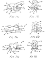
- FIGS 1 to 7 show various embodiments of an integrally formed sheet-metal device 10 for mounting relatively large components, particularly semiconductor heatsinks, to a printed circuit board 12 (pcb).
- pcb printed circuit board 12
- FIG. 1 shows various embodiments of an integrally formed sheet-metal device 10 for mounting relatively large components, particularly semiconductor heatsinks, to a printed circuit board 12 (pcb).
- FIG. 1 shows various embodiments of an integrally formed sheet-metal device 10 for mounting relatively large components, particularly semiconductor heatsinks, to a printed circuit board 12 (pcb).
- FIG. 1 to 7 show various embodiments of an integrally formed sheet-metal device 10 for mounting relatively large components, particularly semiconductor heatsinks, to a printed circuit board 12 (pcb).
- FIG. 1 to 7 show various embodiments of an integrally formed sheet-metal device 10 for mounting relatively large components, particularly semiconductor heatsinks, to a printed circuit board 12 (pcb).
- FIG. 1 to 7 shows various embodiments of an integrally
- Each device includes a sheet-metal member 14 having a head portion 16 for locating in a slot 18 of a component 20 (partially shown in the side views of the figures) to be mounted by the device 10 to a pcb 12.
- Each device 10 also includes a base portion 22 which extends through an aperture 24 formed in the pcb.
- the aperture 24 in the pcb is intended to be generally of standard size as employed for directly mounting normal size components such as integrated circuit chips, transistors or resistors, for example, to the pcb 14 to thus avoid complicating the pcb circuit assembly process.
- the head portion 16 of the device is either formed with a stamped out spade-form member 30 and/or a rolled over spade-form member 32, each of which act in an identical manner to engage in a slot 18 of a component 20.
- the base portion 22 is formed with a stamped out spade-form member 30 and/or a rolled over spade-form member 32.
- the spade-form member (30, 32) of the base portion 22 engages a side wall 28 of an aperture 24 of the pcb 12 and a pull-out force applied to the device 10 causes the spade-form member (30, 32) to imbed firmly into the material of the pcb 12.
- the base portion 22 of the device 10 extends through the aperture 24 and can be soldered by normal techniques, such as the solder bath method, to a reverse surface 36 of the pcb simultaneously with the soldering of other components on the pcb 12.
- the degree to which the spade-form member (30, 32) extends away from the base portion 22 is chosen such that the base portion and spade-form member combination forms a friction fit in an aperture 24 in a pcb 12 thus holding the device 10 in a stable position until the soldering process is complete.
- the spade-form member (30, 32) of the base portion is generally flat across its width. This provides a greater surface area between the spade-form member and aperture surfaces for contact with solder (not shown) than in the conventional case where a component is mounted on a pcb by means of wire-like terminals.
- the base portion 22 may, however, comprise a spade-form member 38 of arcuate form extending in the plane of the sheet-metal member, as shown in figure 3. It will be understood that the base portion can comprise a spade-form member of any suitable shape for securing the device by soldering to a pcb.
- a component 20 such as a semiconductor heatsink can be mounted on a pcb 12 by mounting on the device 10 subsequent to the device having been soldered to the pcb. It is intended that components such as heatsinks are mounted onto the head portion 16 of the device 10 having firstly been formed with a suitably shaped slot in a base part thereof.
- the component 20 can be push-fitted onto the head portion 16 of a mounting device 10 such that the spade-form member (30, 32) of the head portion engages a side wall 26 of the slot in the component.
- the side wall 26 of the slot 18 may have serrations 40 to improve the grip of the head portion in the slot and to increase its resistance to being forcably extracted.
- the spade-form member (30, 32) will possess some resilience which improves the fitting grip and assists in more easily retrieving the component 20 from the device 10.
- Figure 1 shows a first embodiment of the invention. This is of simple form, the head portion 16 having two integrally formed spade-form members 30 stamped from widthwise extending side edge portions 50, both of said spade-form members 30 depending in the same direction away from a face 52 of the head portion 16.
- the base portion 22 of the device has a single integrally formed spade-form member 30, also formed by stamping, which depends outwardly in the same direction as the spade-form members of the head portion.
- the base portion is of lesser width than a central portion 54 of the sheet-metal member extending between the head and base portions. Accordingly, at sides of a line defining the junction between the central and base portions 54, 22), there are provided shoulders 56 which assist in the accurate location of the device 10 on a pcb 12. These shoulders contact with an upper surface 58 of the pcb and thus ensure that the base portion projects through an aperture in the pcb such that an outer edge of the spade-form member engages a side wall of the aperture.
- the device can be positioned ready for soldering on the pcb simultaneously with other components (normally electronic) and by similar methods. Once all components, including component mounting devices, are positioned on the pcb, they can then be secured thereto by passing over a solder bath or by some other suitable soldering method.
- figure 2 is similar to that of figure 1 insofar that it also has a head portion 16 including two spade-form members 32 and a base portion 22 with a single spade-form member 32.
- the width of the base portion 16 is also less than that of the central portion 54.
- the spade-form members 32 of the head portion are formed by bending over top edge portions of side portions of the head portion.
- the spade-form member of the base portion is formed by bending an edge portion but the spade-form members 32 act in identical manner to those of the first embodiment.
- the embodiment of figure 3 is also similar to that of figure 1 but differs in that the base portion 22 has been formed by pressing to provide a single arcuate spade-form member 38 which is adapted to fit in a generally circular aperture in a pcb.
- the shape of the spade-form member 38 is such that it provides a friction fit in the aperture 24 of the pcb 12 with its outer curved surface in contact with a portion of a side wall 28 of said aperture 24.
- Figure 4 illustrates an embodiment of the device in which the head portion 16 has a number of spade-form members 30 arranged in rows.
- the spade-form members are integrally formed by stamping but are arranged such that alternate spade-form members depend from oppositely facing faces of said head portion.
- the oppositely directed spade-form members 30 engage opposing side walls 26 of said slot.
- Such an arrangement can improve the grip between the device and component particularly where both side walls of the slot and the component have serrations 40.
- figure 5 is similar to that of figure 4 insofar that it also has a head portion 16 having a number of rows of spade-form members 30. These also are arranged to depend alternately from oppositely facing faces of the head portion.
- a top edge portion 60 of the head portion is bent over to lie in a plane substantially at right-angles to the plane of the head portion.
- This portion 60 acts to provide a contact zone for manually applying pressure to the device 10 when inserting it on a pcb 12.
- the top edge of the device 10 can be sharp and cause injury when manual pressure is applied on this edge during insertion of the device on the board.
- the bent edge portion 60 provides rigidity in the device in a transverse direction across its width.
- side edge portions 62 of the head portion 16 are bent to lie in a plane at right-angles to the plane of the head portion.
- the bent side edge portions 62 provide rigidity to the device in a depth-wise direction and also improve the stability of the device when inserted on a pcb.
- the bent side edge portions contact on an upper surface 58 of the pcb and act to prevent rotational movement of the device in a direction normal to the plane of the device 10 when a component 20 is being push fitted onto the device.
- the base portion 22 of the device 10 is shown as having or comprising only one spade-form member (30, 32, 38). It will be clearly understood that this portion 22 of the device may be formed with a number of such spade-form members suitably arranged for contact, in use, with a side wall 28 of an aperture 24 on a pcb 12.
- the base portion is shown to be located in an aperture which is generally elongate in shape. It will be understood that the width of the base portion 22 can be reduced in order that the base portion might locate in a standard circular aperture on a pcb.
- Figure 6 shows a sixth embodiment of the invention which has a configuration generally similar to that of the embodiment of figure 5.
- the device has two base portions (22a,b) each formed with a spade-form member 30.
- the spade-form member of the first base portion 22a extends in a direction generally opposite to that of the spade-form member of the second base portion 22b. Therefore, in use, this embodiment of the device can be mounted on a pcb 12 by locating said base portions (22a,b) in separate apertures 24, or alternatively, by locating said base portions in a single elongate aperture whereby said spade-form members each contact with respective opposing side walls of said aperture.
- Figure 7 shows a seventh embodiment of the invention which is generally similar to the embodiment of figure 6.
- this embodiment includes support members 70 extending generally outwardly from the plane of the sheet-metal member 14.
- Each of said support members 70 comprises a first portion 70a extending in a direction normal to the plane of the sheet-metal member 14 and a second portion 70b depending from the first portion in a downward direction generally at right-angles thereto.
- the distal ends 70c of the support members 70 contact with an upper surface 58 of a pcb 12.
- the support members 70 extend from the plane of the sheet-metal member 14 for a distance sufficient to allow a component 20 mounted on the device 10 to rest with its base on the first portions 70a of said support members 70 such that the component is mounted to the pcb spaced above the upper surface 58 thereof.
- the support members facilitate washing of the pcb.
- the support members are integrally formed from the sheet-metal member 14 by stamping from edge portions of said member.
Landscapes
- Engineering & Computer Science (AREA)
- Microelectronics & Electronic Packaging (AREA)
- Structures For Mounting Electric Components On Printed Circuit Boards (AREA)
- Electric Connection Of Electric Components To Printed Circuits (AREA)
- Mounting Components In General For Electric Apparatus (AREA)
Applications Claiming Priority (2)
| Application Number | Priority Date | Filing Date | Title |
|---|---|---|---|
| GB9223064 | 1992-11-04 | ||
| GB929223064A GB9223064D0 (en) | 1992-11-04 | 1992-11-04 | Improvements in electrical component mounting |
Publications (2)
| Publication Number | Publication Date |
|---|---|
| EP0596701A1 true EP0596701A1 (fr) | 1994-05-11 |
| EP0596701B1 EP0596701B1 (fr) | 1998-01-28 |
Family
ID=10724494
Family Applications (1)
| Application Number | Title | Priority Date | Filing Date |
|---|---|---|---|
| EP93308748A Expired - Lifetime EP0596701B1 (fr) | 1992-11-04 | 1993-11-02 | Dispositif de montage sur un plaque à circuits imprimés |
Country Status (4)
| Country | Link |
|---|---|
| US (1) | US5422789A (fr) |
| EP (1) | EP0596701B1 (fr) |
| DE (1) | DE69316709T2 (fr) |
| GB (1) | GB9223064D0 (fr) |
Cited By (2)
| Publication number | Priority date | Publication date | Assignee | Title |
|---|---|---|---|---|
| EP0718932A3 (fr) * | 1994-12-22 | 1997-12-10 | The Whitaker Corporation | Dispositif de maintien en position basse de connecteurs montés sur panneaux |
| EP0735626A3 (fr) * | 1995-03-31 | 1998-02-04 | The Whitaker Corporation | Connecteur électrique avec une fonction de blocage |
Families Citing this family (27)
| Publication number | Priority date | Publication date | Assignee | Title |
|---|---|---|---|---|
| US6280248B1 (en) | 1993-04-19 | 2001-08-28 | Berg Technology, Inc. | Hold-down element for electrical and/or electronic components |
| US5775418A (en) * | 1996-09-20 | 1998-07-07 | Digital Equipment Corporation | T-shaped locking member for engaging a passageway in a heat sink for securement to a mounting board |
| US5987714A (en) * | 1996-10-07 | 1999-11-23 | Smith; Edward John | Spring fastener of high sealing performance |
| US5870285A (en) * | 1996-10-25 | 1999-02-09 | International Business Machines Corporation | Assembly mounting techniques for heat sinks in electronic packaging |
| US5917701A (en) * | 1997-11-05 | 1999-06-29 | Artesyn Technologies, Inc. | Heat sink hold-down clip |
| US6279207B1 (en) | 1999-02-01 | 2001-08-28 | Wtpa, Incorporated | Fasteners with increased holding power |
| US6353981B1 (en) | 1999-02-25 | 2002-03-12 | Termax Corporation | Multi-engagement spring fastener |
| US6139362A (en) * | 1999-07-30 | 2000-10-31 | Berg Technology, Inc. | Fastener for connecting an electrical device to a substrate |
| US6424538B1 (en) * | 2000-10-18 | 2002-07-23 | Compaq Computer Corporation | Mounting protection system for a circuit board |
| US6568045B2 (en) | 2000-12-13 | 2003-05-27 | Termax Corporation | Easily insertable V-shaped sealing fastener |
| US7640634B2 (en) * | 2002-06-07 | 2010-01-05 | Termax Corporation | Ergonomic fastener |
| US7784159B2 (en) * | 2002-06-07 | 2010-08-31 | Termax Corporation | Fastener with ergonomic removal to insertion force ratio |
| US6718599B2 (en) * | 2001-06-25 | 2004-04-13 | Termax Corporation | Spring fastener with ergonomically balanced removal to insertion force ratio |
| US6691380B2 (en) | 2001-07-31 | 2004-02-17 | Eustathios Vassiliou Revocable Trust | Fasteners of increased holding power |
| WO2003100267A1 (fr) | 2002-05-28 | 2003-12-04 | Newfrey Llc | Attache-clip resiliente et son procede de production |
| US6648682B1 (en) * | 2002-07-24 | 2003-11-18 | Hon Hai Precision Ind. Co., Ltd. | Electrical connector having board locks |
| FR2852223B1 (fr) * | 2003-03-11 | 2005-06-10 | Perception Raisonnement Action En Medecine | Instrument de reperage de la position d'un plan de coupe |
| US7188392B2 (en) * | 2003-11-17 | 2007-03-13 | Termax Corporation | Spring fastener with highly improved lever/angle pulling force |
| KR101061108B1 (ko) * | 2003-12-12 | 2011-08-31 | 엘지전자 주식회사 | 비엘디시 모터를 사용하는 세탁기 |
| US8231309B2 (en) * | 2009-12-10 | 2012-07-31 | Willamette Graystone, Inc. | Pier bracket |
| JP2012190561A (ja) * | 2011-03-08 | 2012-10-04 | Fujitsu Ltd | コネクタ固定金具およびコネクタ |
| JP6148489B2 (ja) | 2013-02-13 | 2017-06-14 | 矢崎総業株式会社 | コネクタのペグ圧入構造 |
| AT514072B1 (de) * | 2013-05-13 | 2014-10-15 | Schnabl Stecktechnik Gmbh | Befestigungselement |
| US10894516B2 (en) | 2017-10-18 | 2021-01-19 | Newfrey Llc | U-base fastener with folded barb and multiple spring arms |
| US10704577B2 (en) | 2017-10-18 | 2020-07-07 | Newfrey Llc | U-base fastener with folded barb |
| US11746812B2 (en) | 2021-05-12 | 2023-09-05 | Newfrey Llc | Dual component sealing fastener and coupling assembly including same |
| FR3146970A1 (fr) * | 2023-03-20 | 2024-09-27 | Safran Aircraft Engines | Plaquette d’étanchéité améliorée pour turbine à gaz |
Citations (3)
| Publication number | Priority date | Publication date | Assignee | Title |
|---|---|---|---|---|
| DE7044242U (de) * | 1970-11-30 | 1971-03-11 | Siemens Ag | Aufnahmevorrichtung zur Halterung und Kontaktierung von elektrischen Schaltele menten |
| DE8423052U1 (de) * | 1984-08-02 | 1985-11-28 | Siemens AG, 1000 Berlin und 8000 München | Befestigungsvorrichtung für ein Bauelement, insbesondere ein Relais |
| GB2239135A (en) * | 1989-11-02 | 1991-06-19 | Amp Inc | Mechanical retaining device for electrical connectors |
Family Cites Families (14)
| Publication number | Priority date | Publication date | Assignee | Title |
|---|---|---|---|---|
| US3066367A (en) * | 1957-05-23 | 1962-12-04 | Bishop & Babcock Corp | Panel mounting fastener |
| US3673643A (en) * | 1969-11-19 | 1972-07-04 | Amp Inc | Heat seal retaining clips |
| US4495380A (en) * | 1982-10-08 | 1985-01-22 | Mite Corporation | Combined metal and plastic standoff |
| US4321423A (en) * | 1980-05-15 | 1982-03-23 | Aavid Engineering, Inc. | Heat sink fastenings |
| US4393560A (en) * | 1980-06-28 | 1983-07-19 | Kabushiki Kaisha Togo Seisakusho | Clip for retaining a windshield molding in an automobile |
| US4783899A (en) * | 1984-08-24 | 1988-11-15 | Thermalloy Incorporated | Method of mounting heat sinks |
| US4602315A (en) * | 1984-08-24 | 1986-07-22 | Thermalloy Incorporated | Compensating roll pin for heat sink mounting |
| US4625260A (en) * | 1984-08-24 | 1986-11-25 | Thermalloy Incorporated | Fasteners for surface mounting of printed circuit board components |
| US4964198A (en) * | 1988-09-21 | 1990-10-23 | Avvid Engineering, Inc. | V-shaped clip for attaching a semiconductor device to a heat sink |
| US5015802A (en) * | 1990-08-27 | 1991-05-14 | Enlight Corporation | Computer casing connector |
| US5101540A (en) * | 1991-08-05 | 1992-04-07 | General Motors Corporation | Lamp housing mounting clip |
| US5263233A (en) * | 1991-11-12 | 1993-11-23 | Kim John C | Method and apparatus for flocking an article and the article produced thereby |
| US5145407A (en) * | 1991-11-25 | 1992-09-08 | Amp Incorporated | Mounting device for components |
| US5186517A (en) * | 1992-03-05 | 1993-02-16 | Prince Corporation | Shiftable/releasable mount |
-
1992
- 1992-11-04 GB GB929223064A patent/GB9223064D0/en active Pending
-
1993
- 1993-11-02 US US08/146,323 patent/US5422789A/en not_active Expired - Fee Related
- 1993-11-02 DE DE69316709T patent/DE69316709T2/de not_active Expired - Fee Related
- 1993-11-02 EP EP93308748A patent/EP0596701B1/fr not_active Expired - Lifetime
Patent Citations (3)
| Publication number | Priority date | Publication date | Assignee | Title |
|---|---|---|---|---|
| DE7044242U (de) * | 1970-11-30 | 1971-03-11 | Siemens Ag | Aufnahmevorrichtung zur Halterung und Kontaktierung von elektrischen Schaltele menten |
| DE8423052U1 (de) * | 1984-08-02 | 1985-11-28 | Siemens AG, 1000 Berlin und 8000 München | Befestigungsvorrichtung für ein Bauelement, insbesondere ein Relais |
| GB2239135A (en) * | 1989-11-02 | 1991-06-19 | Amp Inc | Mechanical retaining device for electrical connectors |
Cited By (2)
| Publication number | Priority date | Publication date | Assignee | Title |
|---|---|---|---|---|
| EP0718932A3 (fr) * | 1994-12-22 | 1997-12-10 | The Whitaker Corporation | Dispositif de maintien en position basse de connecteurs montés sur panneaux |
| EP0735626A3 (fr) * | 1995-03-31 | 1998-02-04 | The Whitaker Corporation | Connecteur électrique avec une fonction de blocage |
Also Published As
| Publication number | Publication date |
|---|---|
| EP0596701B1 (fr) | 1998-01-28 |
| US5422789A (en) | 1995-06-06 |
| DE69316709D1 (de) | 1998-03-05 |
| GB9223064D0 (en) | 1992-12-16 |
| DE69316709T2 (de) | 1998-07-16 |
Similar Documents
| Publication | Publication Date | Title |
|---|---|---|
| US5422789A (en) | Printed circuit board component mounting device | |
| JP3238713B2 (ja) | 小型カード・エッジクリップ | |
| EP0855089B1 (fr) | Clip brasable de transistor et puits de chaleur | |
| US4605058A (en) | Heat dissipating retainer for electronic package | |
| US6538197B1 (en) | Conductive member | |
| JP2001522135A (ja) | コンバータソケット端子 | |
| EP0798816A2 (fr) | Dispositif pour fixer d'un connecteur électrique sur une plaquette de circuit imprimé | |
| US4847449A (en) | Alignment apparatus for use in mounting electronic components and heat sinks on circuit boards | |
| JP2001044506A (ja) | 発光ダイオードの固定構造 | |
| US6188131B1 (en) | Clip for retaining a heatsink onto an electronic component | |
| US6923678B2 (en) | Device for temporarily fastening electronic component to circuit board | |
| US6163461A (en) | Terminal mounting structure for a printed circuit board | |
| EP0124715A1 (fr) | Fixation à pince d'un dispositif semi-conducteur à un dissipateur de chaleur | |
| JP2002246085A (ja) | ボトムエントリ型コネクタ | |
| US20040095290A1 (en) | Antenna coupler having a pick-up surface to facilitate surface mounting | |
| US4347552A (en) | Assembly of electrical components with substrates | |
| JP2946059B2 (ja) | 電子部品の取付装置及び取付方法 | |
| US5374205A (en) | Fuse holder | |
| GB2192492A (en) | Alignment device for connecting an electronic component to a printed circuit board | |
| JPS6228797Y2 (fr) | ||
| JPS61193727A (ja) | 電子部品の装着方法 | |
| JPS5932149Y2 (ja) | 配線装置 | |
| US20050160568A1 (en) | Support clip | |
| JPH0129790Y2 (fr) | ||
| JPS6023899Y2 (ja) | プリント配線基板 |
Legal Events
| Date | Code | Title | Description |
|---|---|---|---|
| PUAI | Public reference made under article 153(3) epc to a published international application that has entered the european phase |
Free format text: ORIGINAL CODE: 0009012 |
|
| AK | Designated contracting states |
Kind code of ref document: A1 Designated state(s): DE GB IT |
|
| 17P | Request for examination filed |
Effective date: 19941107 |
|
| 17Q | First examination report despatched |
Effective date: 19960111 |
|
| GRAG | Despatch of communication of intention to grant |
Free format text: ORIGINAL CODE: EPIDOS AGRA |
|
| GRAH | Despatch of communication of intention to grant a patent |
Free format text: ORIGINAL CODE: EPIDOS IGRA |
|
| GRAH | Despatch of communication of intention to grant a patent |
Free format text: ORIGINAL CODE: EPIDOS IGRA |
|
| GRAA | (expected) grant |
Free format text: ORIGINAL CODE: 0009210 |
|
| AK | Designated contracting states |
Kind code of ref document: B1 Designated state(s): DE GB IT |
|
| ITF | It: translation for a ep patent filed | ||
| REF | Corresponds to: |
Ref document number: 69316709 Country of ref document: DE Date of ref document: 19980305 |
|
| PGFP | Annual fee paid to national office [announced via postgrant information from national office to epo] |
Ref country code: DE Payment date: 19981026 Year of fee payment: 6 |
|
| PGFP | Annual fee paid to national office [announced via postgrant information from national office to epo] |
Ref country code: GB Payment date: 19981027 Year of fee payment: 6 |
|
| PLBE | No opposition filed within time limit |
Free format text: ORIGINAL CODE: 0009261 |
|
| 26N | No opposition filed | ||
| PG25 | Lapsed in a contracting state [announced via postgrant information from national office to epo] |
Ref country code: GB Free format text: LAPSE BECAUSE OF NON-PAYMENT OF DUE FEES Effective date: 19991102 |
|
| GBPC | Gb: european patent ceased through non-payment of renewal fee |
Effective date: 19991102 |
|
| PG25 | Lapsed in a contracting state [announced via postgrant information from national office to epo] |
Ref country code: DE Free format text: LAPSE BECAUSE OF NON-PAYMENT OF DUE FEES Effective date: 20000901 |
|
| PG25 | Lapsed in a contracting state [announced via postgrant information from national office to epo] |
Ref country code: IT Free format text: LAPSE BECAUSE OF NON-PAYMENT OF DUE FEES;WARNING: LAPSES OF ITALIAN PATENTS WITH EFFECTIVE DATE BEFORE 2007 MAY HAVE OCCURRED AT ANY TIME BEFORE 2007. THE CORRECT EFFECTIVE DATE MAY BE DIFFERENT FROM THE ONE RECORDED. Effective date: 20051102 |