EP0597441A1 - Microprocesseur à fonction de changement de largeur de bus - Google Patents
Microprocesseur à fonction de changement de largeur de bus Download PDFInfo
- Publication number
- EP0597441A1 EP0597441A1 EP93118142A EP93118142A EP0597441A1 EP 0597441 A1 EP0597441 A1 EP 0597441A1 EP 93118142 A EP93118142 A EP 93118142A EP 93118142 A EP93118142 A EP 93118142A EP 0597441 A1 EP0597441 A1 EP 0597441A1
- Authority
- EP
- European Patent Office
- Prior art keywords
- bus
- data
- width
- external
- microprocessor
- Prior art date
- Legal status (The legal status is an assumption and is not a legal conclusion. Google has not performed a legal analysis and makes no representation as to the accuracy of the status listed.)
- Granted
Links
Images




Classifications
-
- G—PHYSICS
- G06—COMPUTING OR CALCULATING; COUNTING
- G06F—ELECTRIC DIGITAL DATA PROCESSING
- G06F13/00—Interconnection of, or transfer of information or other signals between, memories, input/output devices or central processing units
- G06F13/38—Information transfer, e.g. on bus
- G06F13/40—Bus structure
- G06F13/4004—Coupling between buses
- G06F13/4009—Coupling between buses with data restructuring
- G06F13/4018—Coupling between buses with data restructuring with data-width conversion
-
- G—PHYSICS
- G06—COMPUTING OR CALCULATING; COUNTING
- G06F—ELECTRIC DIGITAL DATA PROCESSING
- G06F13/00—Interconnection of, or transfer of information or other signals between, memories, input/output devices or central processing units
- G06F13/14—Handling requests for interconnection or transfer
- G06F13/16—Handling requests for interconnection or transfer for access to memory bus
- G06F13/1668—Details of memory controller
- G06F13/1678—Details of memory controller using bus width
Definitions
- the present invention relates to a microprocessor which is capable of changing or adjusting data-width according to data-width of external memories to be accessed during memory access operation.
- a conventional microprocessor system consists of a microprocessor having 32 bit bus-width, a ROM of 8 bit bus-width for storing a program including instructions, and 4 RAMs, each having 8 bit bus-width, for temporarily storing data.
- the bus-width conversion circuit 104 shown in Fig.1
- there is a method for adjusting the bus-width difference in which the total number of bit-width of ROMs 103 is 32 bits because the total number of the ROMs 103 is four (8 bitsx4 32 bits).
- the 32 bit data bus 102 may be connected directly to the ROMs 102 in the microprocessor system.
- the microcomputer system uses these four RAMs 106, the data-width of the ROMs 106 becomes 8 bits in the conventional method described above.
- the bit-width of data is decreased, so that the operational performance of the microprocessor system is decreased because the processing function thereof is decreased.
- This function of the microprocessor is called as "dynamic bus sizing function".
- the microprocessor inputs bus-width indication signals per bus cycle in order to repeatedly perform a bus cycle operation for requiring.
- This function is introduced in many kinds of conventional microprocessors, for example MC68020 manufactured by MOTOROLA corporation.
- a microprocessor system including a MPU 107 having the dynamic bus sizing function must have a circuit 109 which is generates a bus-width indication signal corresponding to a data-width of an external memory which is recognized for accessing after decoding an address signal transferred to an address bus 108 in the MPU 107.
- the bus-width indication signals generated from this circuit 109 is transferred to MPU 107 per bus cycle.
- the bus-width indication signals are generated by an address driver 112 for transferring address signals output from the MPU 110 to a memory 111, an address decoder 113 for decoding the output from the address driver 112 and then generates a selection signal CS for selecting the memory 111 to be accessed, and a bus-width indication signal generator 114 for generating bus-width indication signals corresponding to the bit-width of the memory to be selected by the selection signal from the address decoder 112.
- t c y c is an allowable bus cycle time to access the memory 111
- t a is a delay time of address signal output from the MPU 110 in synchronization with a clock signal
- t b is a delay time of an address signal by the address driver 112
- t c is a delay time of the address decoder 113
- t d is a time to be required for generating signals by the generator 114
- t e " is a setting up timing of the bus-width indication signal.
- the setting-up timing for the bus-width indication signal becomes strict and accessing timing for the memory becomes also rigid when the operational frequency such as the clock signal becomes high in order to reduce the bus cycle time. It causes error operation in the microprocessor system.
- a high speed operation of the microprocessor system cannot be achieved because the output condition of the bus-width indication signals is not satisfied.
- microprocessor having a function similar to the dynamic bus sizing function described above is disclosed in the Japanese Patent laid open No.3-98145.
- This microprocessor is capable of dynamically changing a bus-width corresponding to the address of a region to be accessed.
- signal indicatings a bus-width are generated based on an address decoding result like the microprocessor having the dynamic bus sizing function because a bus-width indication signals is generated after comparing the decoding result of an address signal with a specified address.
- the main object of the present invention is to provide a microprocessor which is capable of performing at a high speed rate and adjusting data-width without decreasing processing ability and increasing of a system costs thereof and to avoid decreasing of the margin of operations caused by increasing of an operational frequency thereof.
- a microprocessor having a data-width changing function which accesses instruction and data to external memory means through external data bus means consisting of a plurality of buses which is connected to said microprocessor, which comprising:
- the content of said memory means is re-set by said processor core means based on a program.
- the content of said memory means is set with fixed data when said microprocessor is initialized.
- the content of said memory means may be re-set after initialization for said microprocessor.
- said microprocessor further comprises selection means for selecting the first and second bus-width indication data which is provided from external device of said microprocessor when a re-setting signal is effective, and selecting the first and second bus-width indication data which is transferred from said processor core means, then said microprocessor stores the first and second bus-width indication data selected by said selection means to said memory means as an initial value.
- a microprocessor having a data-width change function which accesses instruction and data to external memory means through external data bus means consisting of a plurality of buses which is connected to said microprocessor, which comprising:
- Fig.7 is a block diagram of a microprocessor as a first embodiment of the present invention.
- the microprocessor is capable of selecting a bus-width at an instruction fetch operation and an operand access operation each according to a specified bus-width which has already stored in an internal register.
- a 32 bit microprocessor or MPU 1 comprises a MPU core section 2 which has a main function of the MPU 1, a control register 3 to store information designating a bus-width, a bus state control circuit 4, an external data bus (DO to D31), an internal data bus (IBO to IB31), and a bus-width change circuit 5 for performing under the control of the bus state control circuit 4.
- a microprocessor system is formed by using the microprocessor 1 above, a ROM of 8 bit bus-width for storing a program, and four RAMs for temporarily storing data.
- the MPU core section 2 can treat address and data of 32 bit-width.
- the MPU core section 2 consists of instruction fetch unit 201, an instruction decode unit 202, and an execution unit 203.
- the instruction fetch unit 201 outputs a bus access type signal BAT of 1 (BAT 1) that indicates instruction fetch operation to the external ROM.
- the control register 3 stores data that indicates a bus-width of the external data bus 6 to actually use for data transfer operation.
- the configuration of the control register 3 is made up of 4 bit fields, as shown in Fig.10.
- the fields RO and R1 are used for indicating a bus-width of the external data bus 6 during the operand access operation.
- One of 8 bit bus-width, the 16 bit bus-width, and 32 bit bus-width is selected based on the contents of the fields RO and R1.
- the fields R2 and R3 are used for indicating a bus-width of the external data bus 6 during the instruction fetch operation.
- One of 8 bit bus-width, the 16 bit bus-width, and 32 bit bus-width is also selected based on the contents of the fields R2 and R3.
- a bus-width indication data is input to the control register 3 from external bus-width indication signal when a reset signal for initializing the microprocessor 1 is asserted.
- the bus-width indication data is input to the control register 3 from the MPU core section 2 through the selector 7.
- an actual bus-width of the external data bus 6 to be accessed is set as an initial value from the bus-width indication signal when the microprocessor 1 is initialized, then during normal operation the content of the control register 3 may be changed by a software program as required.
- the bus state control circuit 4 consists of a bus-width indication signal generator 11 and a bus state control signal generator 12.
- the bus-width indication signal generator 11 generates a bus-width indication signal B8, B16, and B32 based on the contents of the control register 3 (RO to R3) and the bus access type signal BAT.
- the bus state control signal generator 12 generates control signals S2, S4, S6, S8, and S10 for controlling the bus-width change circuit 5, an internal bus cycle completion signal IBDC for indicating the completion of the bus cycle, and an external bus cycle start signal BS for indicating the start of the bus cycle.
- the bus-width indication signal generator 11 for example as shown in Fig.12, consists of logical gates which have the following logic relationship shown in Table 1.
- the bus-width of the external data bus 6 is selected as follows:
- the bus-width of the external data bus 6 is selected as follows:
- the bus state control signal generator 12 generates control signals S2, S4, S6, S8, and S10 in order to control the bus-width change operation for the bus-width change circuit 5 as shown in a state transition diagram in Fig.13.
- each state transits in synchronism with a rising edge of the clock signal.
- a state St1 means a state in which no bus cycle is performed.
- the states St2, St4, St6, St8, and St10 indicate a waiting state in which the current state is kept as long as the external data transfer completion signal (DC) is asserted.
- DC external data transfer completion signal
- the state St1 transits to the state St2 at the first clock, and the state St2 transits to the state St1 at the second clock if the data transfer completion signal DC is asserted as the low level. If the DC is not asserted, then the state St2 transits to itself repeatedly till the DC is asserted at the state. In this case, 32 bit data is transferred at the timing of the state transition St2 to St1.
- the bus-width of the external data bus is set as 16 bit data-width when the bus cycle operation starts at the state St1
- the state St1 transits to the state St2 at the first clock
- the state St2 transits to the state St3 at the second clock if the DC is asserted
- the state St3 transits to the state St4 at the third clock
- the state St4 transits to the state St1 at the fourth clock if the DC is asserted.
- the state transits to itself repeatedly till the DC is asserted at the state.
- each 16 bit data is transferred at the timing of state transition St2 to St3 and St4 to St1. Thereby the entire 32 bit data is transferred completely by 16 bit data each in two external bus cycles.
- the state transition is St1--> St2--> St5--> St6--> St7--> St8--> St9--> St10--> St1.
- each 8 bit data is transferred at the timing of state transition St2 to St5, St6 to St7, St8 to St9, and St10 to St1. Thereby the entire 32 bit data is transferred completely by 8 bit data each in four external bus cycles.
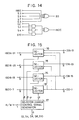
- the external bus cycle start signal (BS) and the internal bus data transfer completion signal (IBDC) are generated by the logic gates as shown in Fig.14.
- the bus-width change circuit 5 consists of selectors 13 to 16 and a selector change control signal generator 17.
- the bus-width change circuit 5 is connected to the internal data bus 8 through a memory data register (MDR) 9.
- MDR memory data register
- the internal data bus 8 is connected to the external data bus 6 every 8 bits.
- the selectors 13 to 16 has a configuration shown in Figs.16 to 19, for example.
- the selector 13 connects the external data bus 6 including DO to D7 with the internal data bus 8 of IBDBO to IBDB7 even if one of 32 bit bus-width, 16 bit bus-width, and 8 bit bus-width is selected based on selector change signals S2R, S2W.
- the selector 13 transfers data read from the external memories through from external data bus of DO to D7 to the internal data bus of IBDBO to IBDB7 when the selector change signal S2R is asserted, and when the selector change signal S2W is asserted data read out from the MPU core section 2 is transferred through from the internal data bus of IBDBO to IBDB7 to the external data bus of DO to D7.
- the selector 14 as shown in Fig.17, connects the external data bus of D8 to D15 with the internal data bus of IBDB8 to IBDB15 when the bus-width of the external data bus 6 is selected as the 32 bit bus-width.
- the selector 14 connects the external data bus of DO to D7 with the internal data bus of IBDB8 to IBDB15 when the bus-width of the external data bus 6 is selected as the 8 bit bus-width.
- the selector 15 as shown in Fig.18, connects the external data bus of D16 to D23 with the internal data bus of IBDB16 to IBDB23 when the bus-width of the external data bus 6 is selected as the 32 bit bus-width.
- the selector 15 connects the external data bus of DO to D7 with the internal data bus of IBDB16 to IBDB23 when the bus-width of the external data bus 6 is selected as the 16 bit or 8 bit bus-width.
- the selector 16 connects the external data bus of D24 to D31 with the internal data bus of IBDB24 to IBDB31 in the buffer transfer state when the bus-width of the external data bus 6 is selected as the 32 bit bus-width.
- the selector 16 connects the external data bus of D8 to D15 with the internal data bus of IBDB24 to IBDB31 when the bus-width of the external data bus 6 is selected as the 16 bit bus-width.
- the selector 16 connects the external data bus of DO to D8 with the internal data bus of IBDB24 to IBDB31 when the bus-width of the external data bus 6 is selected as the bit bus-width.
- the selector change signal generator 17 generates selector change control signals S2R, S2W, S4R, S4W, S6R, S6W, S8R, S8W, S10R, and S10W for controlling the selector change operation for the selectors 13 to 16 shown in Figs.16 to 19.
- This selector change signal generator 17 is made up of the logic gates shown in Fig.20.
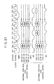
- Fig.21 is a timing chart of the bus cycles of the microprocessor system having the configuration described above.
- the bus access type signal BAT is transferred from the MPU core section 2 to the bus-width indication control generator 11 in the bus state control circuit 4, the bus-width indication signals B8, B16, and B32 are generated based on the bus-width designating data stored in the control register 3.
- the data-width of the external data bus 6 is set as the 32 bit data-width in order to read 32 bit data of A to D from the external memory into the MPU 1, as shown in Fig.21, the internal bus cycle and the external bus cycle for the read operation of the external data is started when the IBBS signal and the BS signal are in the low level. Then, when the state St1 transits to the state St2, data of A to D on the external data bus 6 read-out from the external memory is latched in the memory data register 9 without changing the bus-width of the external data bus 6. This data of A to D in the memory data register 9 is then transferred to the MPU core section 2 through the internal data bus 8.
- the data-width of the external data bus 6 is set as the 16 bit data-width in order to read 32 bit data of E to H from the external memory into the MPU 1, as shown in Fig.21, the internal bus cycle and the external bus cycle for the read operation of the external data is started when the IBBS signal and the BS signal are in the low level.
- E and F (16 bit data) are latched in the lower order 16 bit side of the memory data register 9 through the external data bus DO to D15 and the bus change circuit 4 in the first external bus cycle.
- the data-width of the external data bus 6 is set as the 8 bit data-width in order to read 32 bit data from the external memory into the MPU core section 2, the external data bus 6 and the internal data bus 8 are switched sequentially every 8 bit data transfer for the 32 bit data by the bus change circuit 5 in four by cycles. In this case each 8 bit data in the 32 bit data is transferred sequentially.
- the method of the present invention when comparing with the conventional method described in the prior art section in which a bus-width is determined by an address signal with which an external memory is accessed, the method of the present invention has adequate setting-up timing for the bus-width indication signal. Accordingly, a bus cycle can be executed without operation errors in a case even if the operation frequency becomes high. Therefore the present invention can provide a microprocessor which is capable of performing at a high speed operation.
- This invention is not limited to the embodiment described above. Several modifications of a microprocessor according to the present invention can be available.
- the field configuration of the control register 3 and the configuration of the internal circuits formed in the microprocessor 1 can be changed to another configurations.
- the field configuration RO and R1 registers shown in Fig.10, for the operand data access operation in the control register 3, the operand data field can be further divided into read-out operation and writing operation.
- control register 3 is set by input of an external signal when the re-setting operation is performed in the embodiment described above, there is another method that fixed data values are used, for example 32 bits data for operand access and 8 bit data for instruction fetch access. Further, this fixed values can be also changed after setting the fixed data values.
- each of the data transfer width for instruction fetch operation and the data transfer width for operand access operation may be indicated independently by using external signals. It may be realized by indicating it from external of the MPU 1 instead of input signals RO to R3 to the control register 3.
- the bus-width of an external data bus to be accessed is determined, so that the time for setting the bus-width of the external data bus during a bus cycle is not required. It can be caused to execute the bus cycle in adequate operation margin. Thereby it can be realized to reduce the time of the bus cycle in order to perform a high speed operation.
Landscapes
- Engineering & Computer Science (AREA)
- Theoretical Computer Science (AREA)
- General Engineering & Computer Science (AREA)
- Physics & Mathematics (AREA)
- General Physics & Mathematics (AREA)
- Computer Hardware Design (AREA)
- Bus Control (AREA)
- Microcomputers (AREA)
- Memory System (AREA)
Applications Claiming Priority (3)
| Application Number | Priority Date | Filing Date | Title |
|---|---|---|---|
| JP298526/92 | 1992-11-09 | ||
| JP29852692 | 1992-11-09 | ||
| JP29852692A JP3369227B2 (ja) | 1992-11-09 | 1992-11-09 | プロセッサ |
Publications (2)
| Publication Number | Publication Date |
|---|---|
| EP0597441A1 true EP0597441A1 (fr) | 1994-05-18 |
| EP0597441B1 EP0597441B1 (fr) | 2000-01-26 |
Family
ID=17860871
Family Applications (1)
| Application Number | Title | Priority Date | Filing Date |
|---|---|---|---|
| EP93118142A Expired - Lifetime EP0597441B1 (fr) | 1992-11-09 | 1993-11-09 | Microprocesseur à fonction de changement de largeur de bus |
Country Status (4)
| Country | Link |
|---|---|
| US (1) | US5613078A (fr) |
| EP (1) | EP0597441B1 (fr) |
| JP (1) | JP3369227B2 (fr) |
| DE (1) | DE69327703T2 (fr) |
Cited By (6)
| Publication number | Priority date | Publication date | Assignee | Title |
|---|---|---|---|---|
| EP0786727A1 (fr) * | 1996-01-26 | 1997-07-30 | Motorola, Inc. | Procédé et système de traitement de données pour accéder à un dispositif externe |
| EP0962868A1 (fr) | 1998-06-03 | 1999-12-08 | Lucent Technologies Inc. | Interface de couche physique à largeur de bande échelonnable pour fond de panier |
| JP2002528786A (ja) * | 1998-08-24 | 2002-09-03 | マイクロユニティ システムズ エンジニアリング インコーポレイテッド | ワイド・オペランド・アーキテクチャを含むシステムおよび方法 |
| JP2007531072A (ja) * | 2003-12-19 | 2007-11-01 | マイクロユニティ システムズ エンジニアリング インコーポレイテッド | プログラム可能なプロセッサ及び拡張演算を伴う方法 |
| US7818548B2 (en) | 1995-08-16 | 2010-10-19 | Microunity Systems Engineering, Inc. | Method and software for group data operations |
| US7849291B2 (en) | 1995-08-16 | 2010-12-07 | Microunity Systems Engineering, Inc. | Method and apparatus for performing improved group instructions |
Families Citing this family (48)
| Publication number | Priority date | Publication date | Assignee | Title |
|---|---|---|---|---|
| EP0562151B1 (fr) * | 1992-03-27 | 1998-12-23 | Siemens Aktiengesellschaft | Microprocesseur intégré |
| JPH09231130A (ja) * | 1996-02-26 | 1997-09-05 | Mitsubishi Electric Corp | マイクロコンピュータ |
| DE19636381C1 (de) * | 1996-09-09 | 1998-03-12 | Ibm | Bus mit anforderungsabhängiger Anpassung der in beiden Richtungen zur Verfügung stehenden Bandbreite |
| US5911053A (en) * | 1996-09-30 | 1999-06-08 | Intel Corporation | Method and apparatus for changing data transfer widths in a computer system |
| US6226736B1 (en) * | 1997-03-10 | 2001-05-01 | Philips Semiconductors, Inc. | Microprocessor configuration arrangement for selecting an external bus width |
| US5919254A (en) * | 1997-06-25 | 1999-07-06 | Intel Corporation | Method and apparatus for switching between source-synchronous and common clock data transfer modes in a multiple processing system |
| US7272703B2 (en) * | 1997-08-01 | 2007-09-18 | Micron Technology, Inc. | Program controlled embedded-DRAM-DSP architecture and methods |
| US6427179B1 (en) * | 1997-10-01 | 2002-07-30 | Globespanvirata, Inc. | System and method for protocol conversion in a communications system |
| KR100265362B1 (ko) * | 1997-12-30 | 2000-09-15 | 김영환 | 직병렬 방식을 이용한 마이크로프로세서의 데이터송수신 방법 |
| US6298431B1 (en) * | 1997-12-31 | 2001-10-02 | Intel Corporation | Banked shadowed register file |
| JPH11259238A (ja) * | 1998-03-11 | 1999-09-24 | Matsushita Electric Ind Co Ltd | 信号処理装置 |
| US6202116B1 (en) * | 1998-06-17 | 2001-03-13 | Advanced Micro Devices, Inc. | Write only bus with whole and half bus mode operation |
| DE69942339D1 (de) | 1998-08-24 | 2010-06-17 | Microunity Systems Eng | System mit breiter operandenarchitektur und verfahren |
| US7932911B2 (en) | 1998-08-24 | 2011-04-26 | Microunity Systems Engineering, Inc. | Processor for executing switch and translate instructions requiring wide operands |
| US6611891B1 (en) * | 1998-11-23 | 2003-08-26 | Advanced Micro Devices, Inc. | Computer resource configuration mechanism across a multi-pipe communication link |
| US6510472B1 (en) * | 1999-09-23 | 2003-01-21 | Intel Corporation | Dual input lane reordering data buffer |
| US6609171B1 (en) * | 1999-12-29 | 2003-08-19 | Intel Corporation | Quad pumped bus architecture and protocol |
| US6622194B1 (en) * | 2000-08-28 | 2003-09-16 | Intel Corporation | Efficient use of multiple buses for a scalable and reliable high-bandwidth connection |
| TW507128B (en) * | 2001-07-12 | 2002-10-21 | Via Tech Inc | Data memory controller supporting the data bus invert |
| US7174467B1 (en) | 2001-07-18 | 2007-02-06 | Advanced Micro Devices, Inc. | Message based power management in a multi-processor system |
| US7051218B1 (en) * | 2001-07-18 | 2006-05-23 | Advanced Micro Devices, Inc. | Message based power management |
| JP2003223412A (ja) * | 2002-01-30 | 2003-08-08 | Oki Electric Ind Co Ltd | 半導体集積回路 |
| DE10204344A1 (de) * | 2002-02-01 | 2003-08-14 | Systemonic Ag | Konfigurierbares Bussystem |
| JP4198376B2 (ja) * | 2002-04-02 | 2008-12-17 | Necエレクトロニクス株式会社 | バスシステム及びバスシステムを含む情報処理システム |
| US8832346B2 (en) * | 2003-06-16 | 2014-09-09 | Nvidia Corporation | Data packing and unpacking engine |
| JP2005190092A (ja) * | 2003-12-25 | 2005-07-14 | Matsushita Electric Ind Co Ltd | メモリアクセスコントロール回路 |
| JP4489454B2 (ja) * | 2004-02-16 | 2010-06-23 | 富士通マイクロエレクトロニクス株式会社 | 半導体集積回路 |
| US7366864B2 (en) * | 2004-03-08 | 2008-04-29 | Micron Technology, Inc. | Memory hub architecture having programmable lane widths |
| US7590797B2 (en) * | 2004-04-08 | 2009-09-15 | Micron Technology, Inc. | System and method for optimizing interconnections of components in a multichip memory module |
| JP2005309229A (ja) * | 2004-04-23 | 2005-11-04 | Matsushita Electric Ind Co Ltd | 情報処理装置 |
| US7844767B2 (en) * | 2004-05-21 | 2010-11-30 | Intel Corporation | Method for identifying bad lanes and exchanging width capabilities of two CSI agents connected across a link |
| CN101031900A (zh) * | 2004-07-30 | 2007-09-05 | 皇家飞利浦电子股份有限公司 | 可适应可变外部存储器的大小和字节存储顺序的数据处理设备 |
| US7392331B2 (en) * | 2004-08-31 | 2008-06-24 | Micron Technology, Inc. | System and method for transmitting data packets in a computer system having a memory hub architecture |
| US7328299B2 (en) * | 2004-11-23 | 2008-02-05 | Atmel Corporation | Interface for compressed data transfer between host system and parallel data processing system |
| JP4565090B2 (ja) * | 2005-12-26 | 2010-10-20 | タイヨーエレック株式会社 | 弾球遊技機 |
| US7536490B2 (en) * | 2006-07-20 | 2009-05-19 | Via Technologies, Inc. | Method for link bandwidth management |
| KR100805836B1 (ko) * | 2006-07-26 | 2008-02-21 | 삼성전자주식회사 | 버스 폭 설정 장치, 디스플레이 장치 그리고 버스 폭 설정방법 |
| US7624211B2 (en) * | 2007-06-27 | 2009-11-24 | Micron Technology, Inc. | Method for bus width negotiation of data storage devices |
| US8742791B1 (en) * | 2009-01-31 | 2014-06-03 | Xilinx, Inc. | Method and apparatus for preamble detection for a control signal |
| JP2010287150A (ja) * | 2009-06-15 | 2010-12-24 | Sanyo Electric Co Ltd | データ転送回路 |
| WO2014088802A1 (fr) | 2012-12-06 | 2014-06-12 | Rambus Inc. | Découverte et configuration internes locales de dispositifs sélectionnés individuellement et sélectionnés collectivement |
| BR122016007765B1 (pt) | 2013-03-15 | 2022-03-03 | Intel Corporation | Aparelho em comunicação com controlador de memória de host, aparelho acoplado a um módulo de memória e métodos para formar conjuntos eletrônicos |
| JP2015053095A (ja) * | 2013-09-09 | 2015-03-19 | ソニー株式会社 | メモリ、メモリシステムおよびメモリの制御方法 |
| US9785565B2 (en) | 2014-06-30 | 2017-10-10 | Microunity Systems Engineering, Inc. | System and methods for expandably wide processor instructions |
| US10163508B2 (en) | 2016-02-26 | 2018-12-25 | Intel Corporation | Supporting multiple memory types in a memory slot |
| US10459855B2 (en) | 2016-07-01 | 2019-10-29 | Intel Corporation | Load reduced nonvolatile memory interface |
| US10489056B2 (en) * | 2017-11-09 | 2019-11-26 | Nvidia Corporation | Queue manager for streaming multiprocessor systems |
| CN115221078A (zh) * | 2021-04-14 | 2022-10-21 | 瑞昱半导体股份有限公司 | 数据传输方法与数据处理电路 |
Citations (2)
| Publication number | Priority date | Publication date | Assignee | Title |
|---|---|---|---|---|
| EP0036185A2 (fr) * | 1980-03-19 | 1981-09-23 | Kabushiki Kaisha Toshiba | Système de traitement d'information incorporant une unité de commande arithmétique formée sur une seule puce par application d'un circuit semiconducteur à haute intégration |
| EP0417707A2 (fr) * | 1989-09-11 | 1991-03-20 | Hitachi, Ltd. | Microcalculateur avec registres d'adresses pour commande dynamique de bus |
Family Cites Families (7)
| Publication number | Priority date | Publication date | Assignee | Title |
|---|---|---|---|---|
| KR900007564B1 (ko) * | 1984-06-26 | 1990-10-15 | 모토로라 인코포레이티드 | 동적 버스를 갖는 데이터 처리기 |
| JPS6226561A (ja) * | 1985-07-26 | 1987-02-04 | Toshiba Corp | パ−ソナルコンピユ−タ |
| US5125084A (en) * | 1988-05-26 | 1992-06-23 | Ibm Corporation | Control of pipelined operation in a microcomputer system employing dynamic bus sizing with 80386 processor and 82385 cache controller |
| US5220651A (en) * | 1989-10-11 | 1993-06-15 | Micral, Inc. | Cpu-bus controller for accomplishing transfer operations between a controller and devices coupled to an input/output bus |
| JPH03216776A (ja) * | 1990-01-22 | 1991-09-24 | Mitsubishi Electric Corp | 集積回路装置及びそれにより構成されたマイクロプロセッサ |
| JPH0484253A (ja) * | 1990-07-26 | 1992-03-17 | Mitsubishi Electric Corp | バス幅制御回路 |
| US5191653A (en) * | 1990-12-28 | 1993-03-02 | Apple Computer, Inc. | Io adapter for system and io buses having different protocols and speeds |
-
1992
- 1992-11-09 JP JP29852692A patent/JP3369227B2/ja not_active Expired - Fee Related
-
1993
- 1993-11-09 EP EP93118142A patent/EP0597441B1/fr not_active Expired - Lifetime
- 1993-11-09 DE DE69327703T patent/DE69327703T2/de not_active Expired - Fee Related
-
1995
- 1995-06-01 US US08/456,618 patent/US5613078A/en not_active Expired - Fee Related
Patent Citations (2)
| Publication number | Priority date | Publication date | Assignee | Title |
|---|---|---|---|---|
| EP0036185A2 (fr) * | 1980-03-19 | 1981-09-23 | Kabushiki Kaisha Toshiba | Système de traitement d'information incorporant une unité de commande arithmétique formée sur une seule puce par application d'un circuit semiconducteur à haute intégration |
| EP0417707A2 (fr) * | 1989-09-11 | 1991-03-20 | Hitachi, Ltd. | Microcalculateur avec registres d'adresses pour commande dynamique de bus |
Non-Patent Citations (1)
| Title |
|---|
| ZOCH ET AL.: "68020 DYNAMICALLY ADJUSTS ITS DATA TRANSFERS TO MATCH PERIPHERAL PORTS", ELECTRONIC DESIGN, vol. 33, no. 12, May 1985 (1985-05-01), HASBROUCK HEIGHTS, NEW JERSEY US, pages 219 - 225, XP000718152 * |
Cited By (11)
| Publication number | Priority date | Publication date | Assignee | Title |
|---|---|---|---|---|
| US7818548B2 (en) | 1995-08-16 | 2010-10-19 | Microunity Systems Engineering, Inc. | Method and software for group data operations |
| US7849291B2 (en) | 1995-08-16 | 2010-12-07 | Microunity Systems Engineering, Inc. | Method and apparatus for performing improved group instructions |
| US7987344B2 (en) | 1995-08-16 | 2011-07-26 | Microunity Systems Engineering, Inc. | Multithreaded programmable processor and system with partitioned operations |
| US8001360B2 (en) | 1995-08-16 | 2011-08-16 | Microunity Systems Engineering, Inc. | Method and software for partitioned group element selection operation |
| US8117426B2 (en) | 1995-08-16 | 2012-02-14 | Microunity Systems Engineering, Inc | System and apparatus for group floating-point arithmetic operations |
| EP0786727A1 (fr) * | 1996-01-26 | 1997-07-30 | Motorola, Inc. | Procédé et système de traitement de données pour accéder à un dispositif externe |
| KR100385383B1 (ko) * | 1996-01-26 | 2004-03-31 | 모토로라 인코포레이티드 | 외부디바이스를억세스하기위한데이터처리시스템및그방법 |
| EP0962868A1 (fr) | 1998-06-03 | 1999-12-08 | Lucent Technologies Inc. | Interface de couche physique à largeur de bande échelonnable pour fond de panier |
| AU751233B2 (en) * | 1998-06-03 | 2002-08-08 | Lucent Technologies Inc. | Parallel backplane physical layer interface with scalable data bandwidth |
| JP2002528786A (ja) * | 1998-08-24 | 2002-09-03 | マイクロユニティ システムズ エンジニアリング インコーポレイテッド | ワイド・オペランド・アーキテクチャを含むシステムおよび方法 |
| JP2007531072A (ja) * | 2003-12-19 | 2007-11-01 | マイクロユニティ システムズ エンジニアリング インコーポレイテッド | プログラム可能なプロセッサ及び拡張演算を伴う方法 |
Also Published As
| Publication number | Publication date |
|---|---|
| JPH06149723A (ja) | 1994-05-31 |
| JP3369227B2 (ja) | 2003-01-20 |
| EP0597441B1 (fr) | 2000-01-26 |
| US5613078A (en) | 1997-03-18 |
| DE69327703T2 (de) | 2000-06-15 |
| DE69327703D1 (de) | 2000-03-02 |
Similar Documents
| Publication | Publication Date | Title |
|---|---|---|
| US5613078A (en) | Microprocessor and microprocessor system with changeable effective bus width | |
| US5005121A (en) | Integrated CPU and DMA with shared executing unit | |
| US4894768A (en) | Data processing system with coprocessor | |
| KR100341948B1 (ko) | 제어된버스트메모리액세스기능을갖는데이타처리기및그방법 | |
| EP0464615B1 (fr) | Micro-ordinateur équipé d'un appareil de commande DMA | |
| US4949241A (en) | Microcomputer system including a master processor and a slave processor synchronized by three control lines | |
| US4181934A (en) | Microprocessor architecture with integrated interrupts and cycle steals prioritized channel | |
| KR100335785B1 (ko) | 데이타처리명령의실행 | |
| US5041962A (en) | Computer system with means for regulating effective processing rates | |
| US4274138A (en) | Stored program control system with switching between instruction word systems | |
| US5628018A (en) | Data processing apparatus handling plural divided interruption | |
| US4747045A (en) | Information processing apparatus having an instruction prefetch circuit | |
| EP1063594B1 (fr) | Un gestionnaire d'interruption et un micro-ordinateur comprenant ce gestionnaire | |
| US5696957A (en) | Integrated circuit comprising a central processing unit for executing a plurality of programs | |
| US5386537A (en) | System with reduced instruction set processor accessing plural memories at different speeds using bank interleaving | |
| JP7468112B2 (ja) | インタフェース回路およびインタフェース回路の制御方法 | |
| US6769051B2 (en) | Memory controller and memory control method for controlling an external memory device to be accessible even in an addressing mode that is not supported thereby | |
| US5588124A (en) | Microcomputer | |
| US5742842A (en) | Data processing apparatus for executing a vector operation under control of a master processor | |
| EP0385136B1 (fr) | Microprocesseur coopérant avec un coprocesseur | |
| US5247640A (en) | Dual access control system including plural magnetic disk control units and contention control circuitry | |
| US5487157A (en) | Microprogrammed microcomputer with high-speed interrupt for DRAM refresh | |
| US5677859A (en) | Central processing unit and an arithmetic operation processing unit | |
| US4628450A (en) | Data processing system having a local memory which does not use a directory device with distributed resident programs and a method therefor | |
| US5201052A (en) | System for transferring first and second ring information from program status word register and store buffer |
Legal Events
| Date | Code | Title | Description |
|---|---|---|---|
| PUAI | Public reference made under article 153(3) epc to a published international application that has entered the european phase |
Free format text: ORIGINAL CODE: 0009012 |
|
| 17P | Request for examination filed |
Effective date: 19931109 |
|
| AK | Designated contracting states |
Kind code of ref document: A1 Designated state(s): DE FR GB |
|
| 17Q | First examination report despatched |
Effective date: 19961223 |
|
| GRAG | Despatch of communication of intention to grant |
Free format text: ORIGINAL CODE: EPIDOS AGRA |
|
| GRAG | Despatch of communication of intention to grant |
Free format text: ORIGINAL CODE: EPIDOS AGRA |
|
| GRAH | Despatch of communication of intention to grant a patent |
Free format text: ORIGINAL CODE: EPIDOS IGRA |
|
| GRAH | Despatch of communication of intention to grant a patent |
Free format text: ORIGINAL CODE: EPIDOS IGRA |
|
| GRAA | (expected) grant |
Free format text: ORIGINAL CODE: 0009210 |
|
| AK | Designated contracting states |
Kind code of ref document: B1 Designated state(s): DE FR GB |
|
| REF | Corresponds to: |
Ref document number: 69327703 Country of ref document: DE Date of ref document: 20000302 |
|
| ET | Fr: translation filed | ||
| PLBE | No opposition filed within time limit |
Free format text: ORIGINAL CODE: 0009261 |
|
| STAA | Information on the status of an ep patent application or granted ep patent |
Free format text: STATUS: NO OPPOSITION FILED WITHIN TIME LIMIT |
|
| 26N | No opposition filed | ||
| REG | Reference to a national code |
Ref country code: GB Ref legal event code: IF02 |
|
| PGFP | Annual fee paid to national office [announced via postgrant information from national office to epo] |
Ref country code: DE Payment date: 20051103 Year of fee payment: 13 |
|
| PGFP | Annual fee paid to national office [announced via postgrant information from national office to epo] |
Ref country code: FR Payment date: 20051108 Year of fee payment: 13 |
|
| PGFP | Annual fee paid to national office [announced via postgrant information from national office to epo] |
Ref country code: GB Payment date: 20051109 Year of fee payment: 13 |
|
| PG25 | Lapsed in a contracting state [announced via postgrant information from national office to epo] |
Ref country code: DE Free format text: LAPSE BECAUSE OF NON-PAYMENT OF DUE FEES Effective date: 20070601 |
|
| GBPC | Gb: european patent ceased through non-payment of renewal fee |
Effective date: 20061109 |
|
| REG | Reference to a national code |
Ref country code: FR Ref legal event code: ST Effective date: 20070731 |
|
| PG25 | Lapsed in a contracting state [announced via postgrant information from national office to epo] |
Ref country code: GB Free format text: LAPSE BECAUSE OF NON-PAYMENT OF DUE FEES Effective date: 20061109 |
|
| PG25 | Lapsed in a contracting state [announced via postgrant information from national office to epo] |
Ref country code: FR Free format text: LAPSE BECAUSE OF NON-PAYMENT OF DUE FEES Effective date: 20061130 |