EP0598400A2 - Halbleiterspeicheranordnung - Google Patents
Halbleiterspeicheranordnung Download PDFInfo
- Publication number
- EP0598400A2 EP0598400A2 EP93118578A EP93118578A EP0598400A2 EP 0598400 A2 EP0598400 A2 EP 0598400A2 EP 93118578 A EP93118578 A EP 93118578A EP 93118578 A EP93118578 A EP 93118578A EP 0598400 A2 EP0598400 A2 EP 0598400A2
- Authority
- EP
- European Patent Office
- Prior art keywords
- voltage
- lines
- transistors
- precharge
- data
- Prior art date
- Legal status (The legal status is an assumption and is not a legal conclusion. Google has not performed a legal analysis and makes no representation as to the accuracy of the status listed.)
- Withdrawn
Links
Images




Classifications
-
- G—PHYSICS
- G11—INFORMATION STORAGE
- G11C—STATIC STORES
- G11C11/00—Digital stores characterised by the use of particular electric or magnetic storage elements; Storage elements therefor
- G11C11/21—Digital stores characterised by the use of particular electric or magnetic storage elements; Storage elements therefor using electric elements
- G11C11/34—Digital stores characterised by the use of particular electric or magnetic storage elements; Storage elements therefor using electric elements using semiconductor devices
- G11C11/40—Digital stores characterised by the use of particular electric or magnetic storage elements; Storage elements therefor using electric elements using semiconductor devices using transistors
- G11C11/41—Digital stores characterised by the use of particular electric or magnetic storage elements; Storage elements therefor using electric elements using semiconductor devices using transistors forming static cells with positive feedback, i.e. cells not needing refreshing or charge regeneration, e.g. bistable multivibrator or Schmitt trigger
- G11C11/413—Auxiliary circuits, e.g. for addressing, decoding, driving, writing, sensing, timing or power reduction
- G11C11/417—Auxiliary circuits, e.g. for addressing, decoding, driving, writing, sensing, timing or power reduction for memory cells of the field-effect type
- G11C11/419—Read-write [R-W] circuits
-
- G—PHYSICS
- G11—INFORMATION STORAGE
- G11C—STATIC STORES
- G11C11/00—Digital stores characterised by the use of particular electric or magnetic storage elements; Storage elements therefor
- G11C11/21—Digital stores characterised by the use of particular electric or magnetic storage elements; Storage elements therefor using electric elements
- G11C11/34—Digital stores characterised by the use of particular electric or magnetic storage elements; Storage elements therefor using electric elements using semiconductor devices
- G11C11/40—Digital stores characterised by the use of particular electric or magnetic storage elements; Storage elements therefor using electric elements using semiconductor devices using transistors
- G11C11/41—Digital stores characterised by the use of particular electric or magnetic storage elements; Storage elements therefor using electric elements using semiconductor devices using transistors forming static cells with positive feedback, i.e. cells not needing refreshing or charge regeneration, e.g. bistable multivibrator or Schmitt trigger
- G11C11/413—Auxiliary circuits, e.g. for addressing, decoding, driving, writing, sensing, timing or power reduction
- G11C11/417—Auxiliary circuits, e.g. for addressing, decoding, driving, writing, sensing, timing or power reduction for memory cells of the field-effect type
- G11C11/418—Address circuits
-
- G—PHYSICS
- G11—INFORMATION STORAGE
- G11C—STATIC STORES
- G11C7/00—Arrangements for writing information into, or reading information out from, a digital store
- G11C7/06—Sense amplifiers; Associated circuits, e.g. timing or triggering circuits
Definitions
- This invention relates to a semiconductor memory device and, more particularly, to an random access MOS memory devise of a static type performing a high speed operation with low power consumption.
- MOS transistors used in each memory cell i.e. memory transistors
- MOS transistors used in each memory cell are formed in an as small size as possible for the sake of the integration density so that the load driving capacity of each memory transistor is extremely low, making it difficult to transfer the data quickly to a sense amplifier via a bit line pair.
- each bit line of the bit line pair has a large stray capacitance owing to a large number of memory cells being connected thereto so that the operation of sending the data in the memory elements to the sense amplifier via the bit line pair requires a very long time taking up the major part of the total time far access operation.
- each memory transistor since each memory transistor is extremely small, the node voltages in the memory elements relative to the stored data are sensitive to voltages on the bit line pair. Therefore, it is needed to precharge the bit line pair to a certain voltage preceeding to the access operation in order to prevent the destribution of the stored data, causing a high current consumption.
- a memory cell MC11 in a conventional semiconductor memory device, includes CMOS type inverters 1, 2 whose input nodes and output nodes are mutually connected to each other and N-channel MOS transfer gate transistors 3, 4 having gate electrode connected to a word line 15.
- a pair of lines 17 and 18 are provided as a bit line pair.
- a plurality of the memory cells MC11 a plurality of the word lines 15 and a plural pairs of bit lines 17 and 18, only one set of them is shown in Figure 5 for simplifying the explanation. That is, a memory cell MC11 as described in the above is provided at each intersection of these word lines 15 and the bit line pair 17 and 18.
- the bit lines 17, 18 are connected to a power supply line V D via N-channel type MOS precharge transistors 5, 6 respectively which have gate electrodes connected to a precharge control line 14.
- the bit lines 17, 18 are also selectively connected to data signal lines 17s, 18s via N-channel column selection gate transistors 7, 8 respectively, each of which has its gate electrode connected to a column selection signal line 23.
- a sense amplifier SA is provided to amplify the memory data transferred to the data lines 17s, 18s.
- This sense amplifier consists of a current mirror load circuit formed by P-channel type MOS transistors 11, 12 and N-channel type MOS transistors 9, 10 which have gate electrodes connected to the data lines 17s, 18s and amplify the memory data, and an N-channel type MOS transistor 13 as a current source.
- the read data is output from a node Nout which is a drain node of the transistor 10.
- the current source transistor 13 is connected to a sense amplifier control line 16 which selectively activates the sense amplifier SA.
- the data lines 17s, 18s are also precharged by precharge transistors 25, 26 which have gate electrodes connected to the precharge control line 14.
- the data lines 17s, 18s are further connected to write signal lines WBa, WBb via write gate transistors WGa, WGb respectively, the gates of these transistors being connected to a write control signal line WSW.
- the bit lines 17, 18 and the data lines 17s, 18s are preliminary precharged to the voltage level of V D - V t , wherein the voltage V D and V t are the power source voltage of the device and the threshold voltage of the N-channel transistors 5, 6, 25, 26 respectively, according to a precharge signal PC on the precharge control line 14 during a first period. Then, in a second period, the precharge operation is completed and the sense amplifier SA is activated according to the control signal on the sense amplifier control line 16. Subsequently, the word line 15 and the column selection line 23 are selectively activated to correct the memory cell MC11 to the bit lines 17 and 18 and the data lines 17s, 18s via the column selection transistors 7, 8.
- the voltage difference appears between the nodes 21, 22 in response to the data stored in the memory cell MC11.
- the data is amplified by the sense amplifier SA and output from the output node Nout.
- the write control signal on the control line WSW is at its low level to disconnect the data lines 17s, 18s from the write signal lines WBa, WBb.
- the write control signal line WSW is changed to the high level so that the data lines 17s, 18s are connected to the write signal lines WBa, WBb, respectively, in the second period.
- the voltage level of one of the bit lines 17, 18 is decreased to the ground voltage VS according to write data so that the write data is written into the memory cell MC11.
- Fig. 7 shows another example of conventional memory devices wherein parts equivalent to those in Fig. 5 are shown by identical symbols.
- This device utilizes P-channel transistors 5P, 6P, 25P, 26P as precharge means for precharging the bit lines 17, 18 and the data lines 17s, 18s up to a power supply voltage V D .
- This device further includes P-channel gate transistors 7P, 8P additionally to the N-channel gate transistors 7, 8.
- the read and write operations of this device is nearly the same as the device of Fig. 6 except for the precharge voltage and the input voltage of the sense amplifier SA.
- the bit lines 17, 18 and the data lines 17s, 18s are precharged to the power supply voltage V D so that the input voltages of the sense amplifier SA become the voltage V D and the lower voltage. Therefore, the sense amplifier SA can operate more efficiently than in case of Fig. 6 where the input voltages at nodes 21 and 22 are V D - V t and the lower voltage.
- the precharge level of each line is at V D - V t , so that the voltage difference between the input nodes 21, 22 of the sense amplifier SA are comparatively low, making it difficult for the sense amplifier to sense the voltage difference quickly.
- the threshold voltage of the N-channel transistors is usually about 1.5V, the range of the input voltage levels of the sense amplifier is decreased to lower than 1.5V. This voltage range markedly reduces the sensing ability of the sense amplifier to detect the potential difference on the complementary data lines and thereby increases the access time of the semiconductor memory circuit.
- the memory device is required to operate under a lower power supply voltage such as 2.5V, it is impossible for the sense amplifier to detect the input voltage difference.
- this voltage raise at the low level node is substantially determined as a product of the precharge voltage of the complementary data lines and the ratio of the ON-resistances of the transfer transistor 3, 4 and an N-channel transistor which is used in the inverter 1 or 2. Therefore, the higher the bit lines are precharged, the higher the voltage of the low level node is raised, making it difficult to hold the memory data correctly and the keeping holding margin of the device small.
- the Japanese Patent Laid-Open Publication No. Hei 2-56799 discloses a circuit configuration in which the MOS transistors corresponding to the transistors 3, 4 in memory cell MC11 in Fig. 6 and the MOS transistors corresponding to the transistors 5, 6 for precharging the bit lines 17, 18 in Fig. 6 are replaced by P-channel type MOS transistors and the voltage source for precharging is set at the ground level.
- the precharge level of the bit lines corresponding to the lines 17, 18 are the voltage V t so that the input voltages of the sense amplifier become the voltage V t and a more higher voltage. Therefore the sense amplifier itself can operate more efficiently than in a case of Fig.
- a semiconductor memory device comprises a plurality of word lines, a plurality of pairs of bit lines, a plurality of memory elements each arranged at one of intersections of the word lines and the pairs of bit lines, a pair of data lines each associated with a sense amplifier and selectively connected to one of the pairs of complementary data lines via pair of transfer gates transistors, a first precharge circuit for charging the pairs of bit lines, and a second precharge circuit for charging the pair of data lines, wherein the second precharge circuit charges the pair of data lines to a first voltage and the first precharge circuit charges the pairs of bit lines to a second voltage which is smaller than the first voltage.
- the second voltage is preferably smaller than the first voltage by a threshold voltage of the transfer gate transistors.
- the transfer gate transistors have their gate electrodes is supplied, when selected with the first voltage.
- each of the transfer gate transistors is of an N-channel type, and the first and the second precharge means include N-channel and P-channel MOS type transistors, respectively.
- Fig. 1 is a block diagram of a memory device embodying the present invention.
- Fig. 2 shows a circuit configuration of the important part of the device shown in Fig. 1 according to an embodiment of the invention.
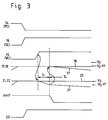
- Fig. 3 is a timing chart in a data read mode of the circuit shown in Fig. 2.
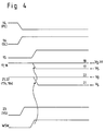
- Fig. 4 is a timing chart in a data write mode of the circuit shown in Fig. 3.
- Fig. 5 is a circuit configuration of a device of another embodiment of the present invention.
- Fig. 6 shows an example of conventional semiconductor memory circuits.
- Fig. 7 shows another example of conventional semiconductor memory circuits.
- a memory device has a memory cell array 101, a word driver 102, a column, selector 103, a bit line precharge circuit 107 and a sensing circuit 104 which comprises a sense amplifier portion 104a and a sense amplifier precharge circuit 104a.
- the device also comprises a write data bus line region 105, a write circuit 106 and a control circuit 108 supplied with a set of address signals Add and control signals (not shown) and outputting a precharge control signal PC to the bit line precharge circuit 107, a sensing control signal SC to the sensing circuit 104, the drive control signals Ax to the word driver 102 and selection control signals YS to the column selector 103, respectively.
- Fig. 2 is a circuit diagram illustrating a part of the memory device of this embodiment, wherein equivalent parts to those in Figs. 5 are designated by reference numerals and identical symbols to omit further description thereof.
- P-channel MOS type precharge transistors 19, 20 are provided for precharging the data lines 17s, 18s and the input nodes 21 and 22 of the sense amplifier SA up to the power supply voltage V D , which is about 3V
- the precharge transistors 5, 6 are formed by N-channel MOS type transistors for precharging the complementary data lines 17, 18 to the voltage V D - V t , wherein the voltage V t is a threshold voltage of each N-channel transistor and about 1.5V.
- the transistors 3, 4 in the memory cell MC11, the column selection transistors 7, 8, the transistors 9, 10, 13 in the sense amplifier SA and the write gate transistors WGa, WGb are also formed by using N-channel transistors.
- the read operation of this device will be described with reference to Fig. 3.
- the set of address signals Add designates the memory cell MC11.
- the precharge control signal PC on the precharge line 14 is preliminary at high level and the bit lines 17 and 18 are precharged by the transistors 5, 6 to V D - V t .
- the sensing control signal SC on the control line 16 is at low level at this time so that the complementary signal lines 17s, 18s and the input nodes 21, 22 of the sense amplifier SA are precharged by the transistors 19, 20 up to the power supply voltage V D .
- the precharge control signal PC goes to the low level to stop the precharge operation on the bit lines 17, 18.
- the control signal SC goes to the high level so that the precharge operation for the signal lines 17s, 18s and the nodes 21, 22 is also completed.
- the column selection signal YS on the control line 23 is activated to the high level according to the address signal Add.
- the transistors 7, 8 are thereby turned on to connect the bit line pair 17, 18 to the data lines 17s, 18s, respectively.
- the precharge level of the bit lines 17, 18 and that of the data lines 17s, 18s are different from each other, that is, the former is V D - V t and the latter is V D , respectively.
- the transistors 7, 8 are of an N-channel type and supplied at the gates thereof with the high level voltage of the control signal SC, which is the power supply voltage V D , charge movement from the data lines 17s, 18s to the bit lines 17, 18 does not occur so that the respective precharging levels are maintained.
- the word line 15 is activated and energized to the high level according to the address signal Add so that the memory cells MC11 is connected to the bit lines 17, 18 via the transistors 3, 4.
- the memory cell MC11 stores data "0" so that the node N1 connected to the transistor 3, is at the low level voltage VS and the node N2 connected to the transistor 4 is at the high level voltage V D .
- one end of the transfer gate transistor 4, which is the node N2 is at V D and the other end thereof, which is the data line 18, is at V D - V t .
- the node N1 within the memory cell MC11 is at the ground voltage VS, the current from the bit line 17 flows to the ground line via the transfer transistor 3 and the N-channel transistor 2TN of the inverter 2, that is, the memory cell MC11 starts to discharge the bit line 17 as well as the data line 17s through the transistor 7.
- the data line 17s is precharged up to the V D level, the precharge voltage V D - V t of the bit line 17 is substantially maintained at the precharge voltage V D - V t until the voltage of the data line 17s (end of the input node 21 of the sense amplifier SA) becomes equal to the voltage level V D - V t .
- the voltage level of the input node 21 of the sense amplifier SA is decreased with the inclination In/Csb during the period T1 from the voltage V D and with the inclination In/(Cb + Csb) during the period T2 as shown in Fig. 3, whereas the voltage level of the data line 17 is not charged during the period T1 and decreased only after the period T1, that is during the period T2, from the precharge voltage V D - V t with the inclination In/(Cb + Csb).
- the sense amplifier SA For the sense amplifier SA, on the other hand, it is required to supply between the input nodes 21, 22 thereof a voltage difference above, about 0.5 to 1V to make the sense amplifies SA sense and amplify the input voltage difference.
- the voltage of the input node 21 of the sense amplifier SA falls to the voltage V D - V t at the end of the first read period T1, making the input voltage difference of the sense amplifier SA as large as the voltage V t . Therefore, it is sufficient for the sense amplifier SA to sense the input potential difference and output the read data OUT from the output node Nout at the time near to the end of the period T1 or, at least, immediately after the period T1.
- the stored data in the memory cell MC11 substantially reflects only on the voltage of the data line 17s (the input node 21 of the sense amplifier SA), so that the data transfer speed is substantially independent from the capacitance Cb of the bit line 17 which is very large because of its length and the large number of the memory cells MC11 being connected thereto.
- the the capacitance Csb of the data line 17s is very small owing to the minute size thereof, the read operation is achieved at considerably high speed.
- the read operation time as large as (Vsen*(Csb+Cb))/In is needed. That is, the operating speed in a read operation according to this memory device is as several tens or a hundred times as high as in case of conventional ones.
- the precharging level of the input nodes 21, 22 of the sense amplifier SA is the power supply voltage V D , there is no decline in the sensing ability of the sense amplifier SA even under the condition where the lower power supply voltage such as 2.5 or 2V is provided. Furthermore, since the precharging level of the bit lines 17, 18 is the voltage V D - V t , the power consumption of the precharging operation can be reduced and there is no possibility of deterioration in the holding ability of the memory cells MC11 to store the low level voltage as a memory data, that is, the holding margin of the memory cells MC11 is highly increased.
- the precharge control signal PC on the precharge line 14 is preliminary at high level and the bit lines 17, 18 are precharged to the voltage V D - V t .
- the sensing control signal SC is at low level and the data lines 17s, 18s and the input nodes 21, 22 of the sense amplifier SA are precharged to the power supply voltage V D .
- the signals PC and SC are changed to the low level and the high level, respectively, to terminate the precharge operation of the respective lines 17, 18, 17s and 18s.
- the column selection signal YS on the line 23 is then activated to the high level so that the bit lines 17, 18 and the data lines 17s, 18s are connected to each other, respectively.
- the precharge levels of the complementary data lines 17, 18 and the signal lines 17s, 18s, which are V D - V t and V D , respectively, are maintained owing to the transistors 7, 8.
- the word line 15 is activated and the memory cell MC11 is thereby connected to the bit lines 17, 18.
- the write control signal line WSW is activated to the high level, so that the true and complementary write data signals indicative of data to be written are transferred via the write data lines WBa, WBb and the write control gate transistors WGa, WGb to the data lines 17s, 18s.
- one of the data lines 17s and 18s and one of the bit lines 17 and 18 are discharged to the ground voltage VS, whereas the other data line and the other bit line 17 are maintained at the precharged voltage levels V D and V D - V t , respectively.
- the desired data is thus written into the cell MC11.
- the signal line 17s has a very small capacitance Csb as mentioned above so that the power consumption for precharging and discharging the signal line 17s is also very small.
- the data line 17 is precharged only up to the voltage V D - V t which is sufficient to restrain the power consumption within a small amount. That is, when the power supply voltage V D is at 3V and the threshold voltage V t is at 1.5V as mentioned above, power consumption according to this embodiment is only half as in the case where the data lines 17, 18 are precharged to the voltage V D .
- a memory device of another embodiment of this invention corresponds to a case where a memory device has a plurality of columns of complementary data line pairs 17 and 18 associated with a single pair of the data lines 17s, 18s and a sense amplifier SA.
- Fig. 5 shows a circuit configuration where two columns of the data lines 17, 18 are provided.
- the transistors 7, 8 and 71, 81 are selectively activated by a column selection signal on the lines 23, 24 so that a desired column of complementary data line pair is selected according to the addess signal Add.
- each complementary data line pair 17 and 18 is precharged to the voltage V D - V t by the N-channel MOS transistors 5, 6 and the signal lines 17s, 18s and the input nodes 21, 22 of the sense amplifier SA are precharged to the voltage V D by the P-channel MOS transistors 11, 12.
- This device also achieves the high speed operation even under the condition of a low power supply voltage and has small power consumption and a large holding margin.
- the circuit configuration of the device according to the invention can be improved in such a manner that the sense amplifier SA is deactivated and the data lines 17, 18 and the signal lines 17s, 18s are precharged immediately after the first read period T1 so as to reduce the power consumption more effectively.
Landscapes
- Engineering & Computer Science (AREA)
- Microelectronics & Electronic Packaging (AREA)
- Computer Hardware Design (AREA)
- Static Random-Access Memory (AREA)
- Dram (AREA)
Applications Claiming Priority (2)
| Application Number | Priority Date | Filing Date | Title |
|---|---|---|---|
| JP4332507A JPH06162776A (ja) | 1992-11-18 | 1992-11-18 | 半導体メモリ回路 |
| JP332507/92 | 1992-11-18 |
Publications (2)
| Publication Number | Publication Date |
|---|---|
| EP0598400A2 true EP0598400A2 (de) | 1994-05-25 |
| EP0598400A3 EP0598400A3 (de) | 1995-03-29 |
Family
ID=18255707
Family Applications (1)
| Application Number | Title | Priority Date | Filing Date |
|---|---|---|---|
| EP93118578A Withdrawn EP0598400A3 (de) | 1992-11-18 | 1993-11-18 | Halbleiterspeicheranordnung. |
Country Status (4)
| Country | Link |
|---|---|
| US (1) | US5418749A (de) |
| EP (1) | EP0598400A3 (de) |
| JP (1) | JPH06162776A (de) |
| KR (1) | KR0150013B1 (de) |
Cited By (2)
| Publication number | Priority date | Publication date | Assignee | Title |
|---|---|---|---|---|
| SG113403A1 (en) * | 2001-07-03 | 2005-08-29 | Agilent Technologies Inc | Low-voltage digital rom circuit and method |
| EP1933326A4 (de) * | 2005-09-09 | 2009-07-01 | Fujitsu Microelectronics Ltd | Integrierte halbleiterschaltung |
Families Citing this family (16)
| Publication number | Priority date | Publication date | Assignee | Title |
|---|---|---|---|---|
| US5859807A (en) * | 1996-01-26 | 1999-01-12 | Hitachi, Ltd. | Semiconductor integrated circuit device having a controlled overdriving circuit |
| JP2996168B2 (ja) * | 1996-02-23 | 1999-12-27 | 日本電気株式会社 | 半導体メモリ集積回路装置 |
| US5999469A (en) * | 1998-03-04 | 1999-12-07 | Lsi Logic Corporation | Sense time reduction using midlevel precharge |
| US6075733A (en) * | 1998-11-23 | 2000-06-13 | Lsi Logic Corporation | Technique for reducing peak current in memory operation |
| JP4251781B2 (ja) * | 2001-03-12 | 2009-04-08 | 富士通マイクロエレクトロニクス株式会社 | プリチャージ回路及びこれを用いた半導体装置 |
| JP4219663B2 (ja) * | 2002-11-29 | 2009-02-04 | 株式会社ルネサステクノロジ | 半導体記憶装置及び半導体集積回路 |
| JP2005174504A (ja) * | 2003-12-15 | 2005-06-30 | Matsushita Electric Ind Co Ltd | 半導体集積回路 |
| KR100869341B1 (ko) * | 2007-04-02 | 2008-11-19 | 주식회사 하이닉스반도체 | 반도체 메모리 소자와 그의 구동 방법 |
| JP5165286B2 (ja) * | 2007-06-26 | 2013-03-21 | ルネサスエレクトロニクス株式会社 | 半導体記憶装置 |
| JP5055100B2 (ja) * | 2007-12-07 | 2012-10-24 | ラピスセミコンダクタ株式会社 | 半導体記憶装置 |
| JP4844619B2 (ja) * | 2008-03-27 | 2011-12-28 | 株式会社デンソー | 半導体メモリ装置 |
| JP5676075B2 (ja) * | 2008-11-17 | 2015-02-25 | ピーエスフォー ルクスコ エスエイアールエルPS4 Luxco S.a.r.l. | 半導体装置 |
| JP5306084B2 (ja) * | 2009-07-10 | 2013-10-02 | 株式会社東芝 | 半導体記憶装置 |
| JP5741965B2 (ja) | 2010-09-02 | 2015-07-01 | 株式会社ソシオネクスト | データ伝送回路及びそれを備えた半導体記憶装置 |
| JP5789803B2 (ja) * | 2011-12-06 | 2015-10-07 | 株式会社ソシオネクスト | 半導体メモリおよびシステム |
| KR101543701B1 (ko) | 2014-12-22 | 2015-08-12 | 연세대학교 산학협력단 | 감지 증폭기 및 그를 이용한 반도체 메모리 장치 |
Family Cites Families (10)
| Publication number | Priority date | Publication date | Assignee | Title |
|---|---|---|---|---|
| JPS57127989A (en) * | 1981-02-02 | 1982-08-09 | Hitachi Ltd | Mos static type ram |
| JPS61239493A (ja) * | 1985-04-05 | 1986-10-24 | Fujitsu Ltd | 半導体記憶装置 |
| US4661931A (en) * | 1985-08-05 | 1987-04-28 | Motorola, Inc. | Asynchronous row and column control |
| US4802129A (en) * | 1987-12-03 | 1989-01-31 | Motorola, Inc. | RAM with dual precharge circuit and write recovery circuitry |
| JP2704885B2 (ja) * | 1988-08-03 | 1998-01-26 | 株式会社日立製作所 | 半導体記憶装置 |
| JPH0256799A (ja) * | 1988-08-22 | 1990-02-26 | Nippon Telegr & Teleph Corp <Ntt> | メモリ回路 |
| JPH0294096A (ja) * | 1988-09-29 | 1990-04-04 | Mitsubishi Electric Corp | 半導体記憶回路 |
| JPH02154393A (ja) * | 1988-12-06 | 1990-06-13 | Mitsubishi Electric Corp | 半導体記憶回路 |
| JPH0814989B2 (ja) * | 1989-05-09 | 1996-02-14 | 日本電気株式会社 | 内部同期型スタティックram |
| JP2680939B2 (ja) * | 1991-03-27 | 1997-11-19 | 日本電気アイシーマイコンシステム株式会社 | 半導体記憶装置 |
-
1992
- 1992-11-18 JP JP4332507A patent/JPH06162776A/ja active Pending
-
1993
- 1993-11-18 EP EP93118578A patent/EP0598400A3/de not_active Withdrawn
- 1993-11-18 KR KR1019930024597A patent/KR0150013B1/ko not_active Expired - Fee Related
- 1993-11-18 US US08/153,961 patent/US5418749A/en not_active Expired - Fee Related
Cited By (2)
| Publication number | Priority date | Publication date | Assignee | Title |
|---|---|---|---|---|
| SG113403A1 (en) * | 2001-07-03 | 2005-08-29 | Agilent Technologies Inc | Low-voltage digital rom circuit and method |
| EP1933326A4 (de) * | 2005-09-09 | 2009-07-01 | Fujitsu Microelectronics Ltd | Integrierte halbleiterschaltung |
Also Published As
| Publication number | Publication date |
|---|---|
| KR0150013B1 (ko) | 1998-10-01 |
| JPH06162776A (ja) | 1994-06-10 |
| US5418749A (en) | 1995-05-23 |
| KR940012633A (ko) | 1994-06-24 |
| EP0598400A3 (de) | 1995-03-29 |
Similar Documents
| Publication | Publication Date | Title |
|---|---|---|
| US5566120A (en) | Apparatus and method for controlling transistor current leakage | |
| US5581500A (en) | Memory cell with power supply induced reversed-bias pass transistors for reducing off-leakage current | |
| US4616342A (en) | Semiconductor memory device | |
| US5418749A (en) | Semiconductor memory device | |
| US4747082A (en) | Semiconductor memory with automatic refresh means | |
| US4601017A (en) | Semiconductor memory device having active pull-up circuits | |
| JP2611504B2 (ja) | 半導体メモリ | |
| US4062000A (en) | Current sense amp for static memory cell | |
| US4876669A (en) | MOS static type RAM having a variable load | |
| US6081461A (en) | Circuit and method for a memory device with p-channel isolation gates | |
| KR910009442B1 (ko) | 반도체 기억장치 | |
| US4969125A (en) | Asynchronous segmented precharge architecture | |
| US5208773A (en) | Semiconductor memory device having bit lines and word lines different in data reading and data writing | |
| US5796651A (en) | Memory device using a reduced word line voltage during read operations and a method of accessing such a memory device | |
| US6859386B2 (en) | Semiconductor memory device with memory cell having low cell ratio | |
| EP0454061B1 (de) | Dynamische Direktzugriffspeicheranordnung mit verbesserter Speisespannung für eine beschleunigte Wiedereinschreibung von von Speicherzellen gelesenen Informationsbits | |
| US5553028A (en) | Single P-sense AMP circuit using depletion isolation devices | |
| EP0259862A1 (de) | Halbleiterspeicher mit Schreibfunktion | |
| KR100456990B1 (ko) | 반도체기억장치 및 이를 사용한 정보기기 | |
| US6201758B1 (en) | Semiconductor memory device permitting time required for writing data to be reduced | |
| US6067264A (en) | High speed semiconductor memory device | |
| US4610002A (en) | Dynamic memory circuit with improved noise-prevention circuit arrangement for word lines | |
| US7336522B2 (en) | Apparatus and method to reduce undesirable effects caused by a fault in a memory device | |
| EP0451000B1 (de) | Halbleiter-Speichereinrichtung mit verbesserter Kontrollfunktion für Datenbusse | |
| KR101317874B1 (ko) | 불휘발성 기억장치 및 그 판독방법 |
Legal Events
| Date | Code | Title | Description |
|---|---|---|---|
| PUAI | Public reference made under article 153(3) epc to a published international application that has entered the european phase |
Free format text: ORIGINAL CODE: 0009012 |
|
| AK | Designated contracting states |
Kind code of ref document: A2 Designated state(s): DE FR GB IT NL |
|
| PUAL | Search report despatched |
Free format text: ORIGINAL CODE: 0009013 |
|
| AK | Designated contracting states |
Kind code of ref document: A3 Designated state(s): DE FR GB IT NL |
|
| 17P | Request for examination filed |
Effective date: 19950217 |
|
| 17Q | First examination report despatched |
Effective date: 19970402 |
|
| STAA | Information on the status of an ep patent application or granted ep patent |
Free format text: STATUS: THE APPLICATION IS DEEMED TO BE WITHDRAWN |
|
| 18D | Application deemed to be withdrawn |
Effective date: 19980428 |