EP0598596A1 - Mémoire ferro-électrique non-volatile avec des lignes de bit repliées et procédé de fabrication - Google Patents
Mémoire ferro-électrique non-volatile avec des lignes de bit repliées et procédé de fabrication Download PDFInfo
- Publication number
- EP0598596A1 EP0598596A1 EP93309145A EP93309145A EP0598596A1 EP 0598596 A1 EP0598596 A1 EP 0598596A1 EP 93309145 A EP93309145 A EP 93309145A EP 93309145 A EP93309145 A EP 93309145A EP 0598596 A1 EP0598596 A1 EP 0598596A1
- Authority
- EP
- European Patent Office
- Prior art keywords
- lines
- line
- plate
- row
- transistor
- Prior art date
- Legal status (The legal status is an assumption and is not a legal conclusion. Google has not performed a legal analysis and makes no representation as to the accuracy of the status listed.)
- Granted
Links
Images



Classifications
-
- G—PHYSICS
- G11—INFORMATION STORAGE
- G11C—STATIC STORES
- G11C11/00—Digital stores characterised by the use of particular electric or magnetic storage elements; Storage elements therefor
- G11C11/21—Digital stores characterised by the use of particular electric or magnetic storage elements; Storage elements therefor using electric elements
- G11C11/22—Digital stores characterised by the use of particular electric or magnetic storage elements; Storage elements therefor using electric elements using ferroelectric elements
-
- H—ELECTRICITY
- H10—SEMICONDUCTOR DEVICES; ELECTRIC SOLID-STATE DEVICES NOT OTHERWISE PROVIDED FOR
- H10B—ELECTRONIC MEMORY DEVICES
- H10B53/00—Ferroelectric RAM [FeRAM] devices comprising ferroelectric memory capacitors
Definitions
- This invention relates to a non-volatile ferroelectric memory, and more particularly to a non-volatile ferroelectric memory having a folded bit line architecture.
- the conventional (i.e., volatile) DRAM cell includes a pass transistor and a linear dielectric capacitor for storing data.
- a conventional DRAM cell does not rely on remanent polarization or polarization state of a ferroelectric dielectric in the capacitor as the storage mechanism, but relies instead on the charge stored in the capacitor.
- a conventional DRAM cell is interconnected with two controllable lines: a bit line and a word line. Where field effect transistors are used, the bit line is coupled usually to the drain of the transistor and the word line is coupled to the control electrode of the transistor.
- the source of the (pass) transistor is connected to the top electrode of the capacitor, and the bottom electrode of the capacitor is usually grounded or connected to the bottom electrodes of the capacitors of all of the cells in the memory and to ground.
- the noise interference associated with the open bit architecture of the prior art is apparent in view of the block diagram in Figure 3a showing the positioning of the sense amp and the memory cells in the memory.
- the bit line and the bit ⁇ line associated with a sense amplifier are on opposite sides of the sense amplifier. Therefore, noise may be induced on one side of the sense amplifier, for example on the bit line, and not induced on the other side of the sense amplifier, on the bit ⁇ line.
- memories may be considered employing folded bit line architecture as shown in the block diagram of Figure 4a.
- a sense amplifier compares the state (polarization of ferroelectric material) of the bit line to the state of the bit ⁇ line, on the same side of the sense amplifier, to determine the polarization of the ferroelectric material (representing data - - for example, a binary "1") in the memory cell.
- a further object of the invention is to provide a non-volatile ferroelectric memory with folded bit line architecture.
- the word line and plate line coupled to any single cell are not coincident Further, adjacent cells in any row do not share the same word line or plate line, but are connected to the other word line or plate line associated with the row. This pattern continues for all cells in a matrix defined by any given number of cells in a row or column.
- the present design results in a non-volatile ferroelectric memory having a folded bit architecture with reduced size relative to the folded bit line memory of Figure 4b.
- Fig. 1 is a schematic diagram of a conventional DRAM cell.
- Fig. 2 is a schematic diagram of a conventional non-volatile ferroelectric cell.
- Fig. 3b is a representative plan view of part of a conventional non-volatile ferroelectric memory array having open bit lines.
- Fig. 4b is a representative plan view of part of a conventional non-volatile ferroelectric memory array having folded bit lines.
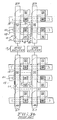
- Fig. 5 is a representative plan view of the non-volatile ferroelectric memory array portion having folded bit lines according to the present invention.
- Figs. 6a-g are cross-sections of a single memory cell of the present invention shown in Fig. 5 (taken at lines 6-6) and show the application of the various layers in making a single memory cell. It is to be understood that the various layers and structures shown in Figures 6 are representative of the layout or structure of the device and are not necessarily drawn to scale.
- the layer for the top electrode 36 which is preferably platinum or a conductive oxide, is deposited by sputtering.
- the top electrode which has a thickness of approximately 500 ⁇ to 3000 ⁇ , completes the ferroelectric capacitor 30.
- a second insulating layer 50 is applied over the newly formed capacitor 30 and the oxide layer 24 over the transistor.
- the second insulating layer 50 is applied by chemical vapor deposition (CVD) to a thickness approximately between 2000 ⁇ and 6000 ⁇ .
- CVD chemical vapor deposition
- a top electrode contact aperture 54 and source and drain contact apertures 56 and 58 are simultaneously etched.
Landscapes
- Engineering & Computer Science (AREA)
- Computer Hardware Design (AREA)
- Semiconductor Memories (AREA)
- Non-Volatile Memory (AREA)
- Dram (AREA)
Applications Claiming Priority (2)
| Application Number | Priority Date | Filing Date | Title |
|---|---|---|---|
| US07/977,825 US5371699A (en) | 1992-11-17 | 1992-11-17 | Non-volatile ferroelectric memory with folded bit lines and method of making the same |
| US977825 | 1992-11-17 |
Publications (2)
| Publication Number | Publication Date |
|---|---|
| EP0598596A1 true EP0598596A1 (fr) | 1994-05-25 |
| EP0598596B1 EP0598596B1 (fr) | 1997-09-10 |
Family
ID=25525560
Family Applications (1)
| Application Number | Title | Priority Date | Filing Date |
|---|---|---|---|
| EP93309145A Expired - Lifetime EP0598596B1 (fr) | 1992-11-17 | 1993-11-16 | Mémoire ferro-électrique non-volatile avec des lignes de bit repliées et procédé de fabrication |
Country Status (4)
| Country | Link |
|---|---|
| US (1) | US5371699A (fr) |
| EP (1) | EP0598596B1 (fr) |
| JP (1) | JP3174209B2 (fr) |
| DE (1) | DE69313785T2 (fr) |
Cited By (4)
| Publication number | Priority date | Publication date | Assignee | Title |
|---|---|---|---|---|
| EP0730276A1 (fr) * | 1995-02-27 | 1996-09-04 | Motorola, Inc. | Réseau de mémoire non-volatile à accèss aléatoire |
| SG79200A1 (en) * | 1995-08-21 | 2001-03-20 | Matsushita Electric Industrial Co Ltd | Ferroelectric memory devices and method for testing them |
| EP0834913A4 (fr) * | 1996-04-19 | 2001-09-05 | Matsushita Electronics Corp | Dispositif pour semi-conducteur |
| DE19846264B4 (de) * | 1997-12-12 | 2007-03-29 | LG Semicon Co., Ltd., Cheongju | Speicherzelleneinheit für einen nichtflüchtigen ferroelektrischen Speicher, nichtflüchtiger ferroelektrischer Speicher mit einer Vielzahl dieser Zellen, Wortleitungstreiber für denselben sowie Verfahren zur Herstellung dieser Zellen |
Families Citing this family (30)
| Publication number | Priority date | Publication date | Assignee | Title |
|---|---|---|---|---|
| US5777356A (en) * | 1996-01-03 | 1998-07-07 | Bell Communications Research, Inc. | Platinum-free ferroelectric memory cell with intermetallic barrier layer and method of making same |
| JP2953369B2 (ja) * | 1996-01-17 | 1999-09-27 | 日本電気株式会社 | 半導体装置の構造およびその製造方法 |
| US5760433A (en) * | 1996-05-31 | 1998-06-02 | Hughes Electronics | In situ reactive layers for protection of ferroelectric integrated circuits |
| KR100197566B1 (ko) * | 1996-06-29 | 1999-06-15 | 윤종용 | 강유전체 메모리 장치 |
| KR100224673B1 (ko) * | 1996-12-13 | 1999-10-15 | 윤종용 | 불휘발성 강유전체 메모리장치 및 그의 구동방법 |
| US6097624A (en) | 1997-09-17 | 2000-08-01 | Samsung Electronics Co., Ltd. | Methods of operating ferroelectric memory devices having reconfigurable bit lines |
| JP3039420B2 (ja) | 1997-02-14 | 2000-05-08 | 日本電気株式会社 | 半導体メモリ |
| US6115281A (en) * | 1997-06-09 | 2000-09-05 | Telcordia Technologies, Inc. | Methods and structures to cure the effects of hydrogen annealing on ferroelectric capacitors |
| KR100297874B1 (ko) | 1997-09-08 | 2001-10-24 | 윤종용 | 강유전체랜덤액세스메모리장치 |
| US6128213A (en) * | 1997-12-12 | 2000-10-03 | Lg Semicon Co., Ltd. | Nonvolatile ferroelectric memory and a method of manufacturing the same |
| US6091624A (en) * | 1997-12-12 | 2000-07-18 | Lg Semicon Co., Ltd. | SWL ferroelectric memory and circuit for driving the same |
| KR100268908B1 (ko) * | 1998-04-22 | 2000-10-16 | 김영환 | 에스더블유엘(swl) 강유전체 메모리 장치 및 그 구동회로 |
| US6091623A (en) * | 1997-12-12 | 2000-07-18 | Lg Semicon Co., Ltd. | Split word line ferroelectric memory |
| US6072711A (en) * | 1997-12-12 | 2000-06-06 | Lg Semicon Co., Ltd. | Ferroelectric memory device without a separate cell plate line and method of making the same |
| US6418043B1 (en) | 1997-12-12 | 2002-07-09 | Hyundai Electronics Industries Co., Ltd. | Circuit for driving nonvolatile ferroelectric memory |
| US6125051A (en) * | 1997-12-12 | 2000-09-26 | Hyundai Electronics Industries Co., Ltd. | Circuit for driving nonvolatile ferroelectric memory |
| KR100268947B1 (ko) * | 1998-04-03 | 2000-10-16 | 김영환 | 비휘발성 강유전체 메모리 및 그의 제어회로 |
| KR100268875B1 (ko) | 1998-05-13 | 2000-10-16 | 김영환 | 비휘발성 강유전체 메모리소자의 구동회로 |
| KR100281125B1 (ko) * | 1998-12-29 | 2001-03-02 | 김영환 | 비휘발성 강유전체 메모리장치 |
| US6215692B1 (en) | 1998-05-13 | 2001-04-10 | Hyundai Electronics Industries Co., Ltd. | Non-volatile ferroelectric memory |
| KR100298439B1 (ko) * | 1998-06-30 | 2001-08-07 | 김영환 | 비휘발성 강유전체 메모리 |
| US6255157B1 (en) | 1999-01-27 | 2001-07-03 | International Business Machines Corporation | Method for forming a ferroelectric capacitor under the bit line |
| US6611014B1 (en) | 1999-05-14 | 2003-08-26 | Kabushiki Kaisha Toshiba | Semiconductor device having ferroelectric capacitor and hydrogen barrier film and manufacturing method thereof |
| DE19948571A1 (de) | 1999-10-08 | 2001-04-19 | Infineon Technologies Ag | Speicheranordnung |
| KR100317331B1 (ko) * | 1999-11-11 | 2001-12-24 | 박종섭 | 불휘발성 강유전체 메모리 소자 및 그 제조방법 |
| KR101450254B1 (ko) * | 2008-07-09 | 2014-10-13 | 삼성전자주식회사 | 증가된 정전 용량을 갖는 스토리지 노드를 포함하는 반도체메모리 소자 |
| JP2010040904A (ja) * | 2008-08-07 | 2010-02-18 | Nec Electronics Corp | 半導体装置及びその製造方法 |
| US20100327877A1 (en) * | 2009-06-24 | 2010-12-30 | Hynix Semiconductor Inc. | Radio frequency identification (rfid) device and method for testing the same |
| KR101087934B1 (ko) * | 2010-03-26 | 2011-11-28 | 주식회사 하이닉스반도체 | Rfid 장치 |
| US9425085B2 (en) * | 2014-05-05 | 2016-08-23 | Taiwan Semiconductor Manufacturing Company Limited | Structures, devices and methods for memory devices |
Citations (1)
| Publication number | Priority date | Publication date | Assignee | Title |
|---|---|---|---|---|
| DE4118847A1 (de) * | 1990-06-08 | 1991-12-12 | Toshiba Kawasaki Kk | Halbleiterspeicheranordnung mit ferroelektrischem kondensator |
Family Cites Families (4)
| Publication number | Priority date | Publication date | Assignee | Title |
|---|---|---|---|---|
| US4491936A (en) | 1982-02-08 | 1985-01-01 | Mostek Corporation | Dynamic random access memory cell with increased signal margin |
| US4873664A (en) * | 1987-02-12 | 1989-10-10 | Ramtron Corporation | Self restoring ferroelectric memory |
| KR950000156B1 (ko) * | 1989-02-08 | 1995-01-10 | 세이꼬 엡슨 가부시끼가이샤 | 반도체 장치 |
| US5070385A (en) * | 1989-10-20 | 1991-12-03 | Radiant Technologies | Ferroelectric non-volatile variable resistive element |
-
1992
- 1992-11-17 US US07/977,825 patent/US5371699A/en not_active Expired - Lifetime
-
1993
- 1993-11-12 JP JP28359493A patent/JP3174209B2/ja not_active Expired - Fee Related
- 1993-11-16 DE DE69313785T patent/DE69313785T2/de not_active Expired - Fee Related
- 1993-11-16 EP EP93309145A patent/EP0598596B1/fr not_active Expired - Lifetime
Patent Citations (1)
| Publication number | Priority date | Publication date | Assignee | Title |
|---|---|---|---|---|
| DE4118847A1 (de) * | 1990-06-08 | 1991-12-12 | Toshiba Kawasaki Kk | Halbleiterspeicheranordnung mit ferroelektrischem kondensator |
Cited By (4)
| Publication number | Priority date | Publication date | Assignee | Title |
|---|---|---|---|---|
| EP0730276A1 (fr) * | 1995-02-27 | 1996-09-04 | Motorola, Inc. | Réseau de mémoire non-volatile à accèss aléatoire |
| SG79200A1 (en) * | 1995-08-21 | 2001-03-20 | Matsushita Electric Industrial Co Ltd | Ferroelectric memory devices and method for testing them |
| EP0834913A4 (fr) * | 1996-04-19 | 2001-09-05 | Matsushita Electronics Corp | Dispositif pour semi-conducteur |
| DE19846264B4 (de) * | 1997-12-12 | 2007-03-29 | LG Semicon Co., Ltd., Cheongju | Speicherzelleneinheit für einen nichtflüchtigen ferroelektrischen Speicher, nichtflüchtiger ferroelektrischer Speicher mit einer Vielzahl dieser Zellen, Wortleitungstreiber für denselben sowie Verfahren zur Herstellung dieser Zellen |
Also Published As
| Publication number | Publication date |
|---|---|
| DE69313785T2 (de) | 1998-04-09 |
| JPH06209113A (ja) | 1994-07-26 |
| US5371699A (en) | 1994-12-06 |
| JP3174209B2 (ja) | 2001-06-11 |
| DE69313785D1 (de) | 1997-10-16 |
| EP0598596B1 (fr) | 1997-09-10 |
Similar Documents
| Publication | Publication Date | Title |
|---|---|---|
| EP0598596B1 (fr) | Mémoire ferro-électrique non-volatile avec des lignes de bit repliées et procédé de fabrication | |
| US6635918B1 (en) | Semiconductor integrated circuit device and method for manufacturing the same | |
| US5047817A (en) | Stacked capacitor for semiconductor memory device | |
| US6141238A (en) | Dynamic random access memory (DRAM) cells with repressed ferroelectric memory methods of reading same, and apparatuses including same | |
| US6337805B1 (en) | Discrete devices including EAPROM transistor and NVRAM memory cell with edge defined ferroelectric capacitance, methods for operating same, and apparatuses including same | |
| US6967365B2 (en) | Ferroelectric memory cell with angled cell transistor active region and methods for fabricating the same | |
| US5436477A (en) | Semiconductor memory device with high dielectric capacitor structure | |
| US6700146B2 (en) | Semiconductor memory device and method for producing the same | |
| US6867447B2 (en) | Ferroelectric memory cell and methods for fabricating the same | |
| US5644151A (en) | Semiconductor memory device and method for fabricating the same | |
| JPH08111510A (ja) | 半導体装置 | |
| US6300654B1 (en) | Structure of a stacked memory cell, in particular a ferroelectric cell | |
| US7456457B2 (en) | Layout of semiconductor memory device and method of controlling capacitance of dummy cell | |
| US5684315A (en) | Semiconductor memory device including memory cells each having an information storage capacitor component formed over control electrode of cell selecting transistor | |
| US20010051414A1 (en) | Semiconductor integrated circuit and method for manufacturing the same | |
| US7439129B2 (en) | Methods for fabricating ferroelectric memory devices | |
| US5180683A (en) | Method of manufacturing stacked capacitor type semiconductor memory device | |
| US20040232457A1 (en) | Memory architecture with series grouped by cells | |
| US20040173826A1 (en) | Ferroelectric memory device and method for manufacturing the same | |
| EP1514275A1 (fr) | Memoire ferroelectrique a cellules de memoire connectees en serie | |
| US7049646B2 (en) | Capacitor for semiconductor integrated devices | |
| US20040056287A1 (en) | Series memory architecture | |
| US6084261A (en) | DRAM cell with a fork-shaped capacitor | |
| JPH0982904A (ja) | ダイナミック型メモリ及びその製造方法 | |
| KR100195262B1 (ko) | 강유전체 메모리 장치 및 그 제조 방법 |
Legal Events
| Date | Code | Title | Description |
|---|---|---|---|
| PUAI | Public reference made under article 153(3) epc to a published international application that has entered the european phase |
Free format text: ORIGINAL CODE: 0009012 |
|
| AK | Designated contracting states |
Kind code of ref document: A1 Designated state(s): DE FR GB |
|
| 17P | Request for examination filed |
Effective date: 19941004 |
|
| 17Q | First examination report despatched |
Effective date: 19961118 |
|
| GRAG | Despatch of communication of intention to grant |
Free format text: ORIGINAL CODE: EPIDOS AGRA |
|
| GRAG | Despatch of communication of intention to grant |
Free format text: ORIGINAL CODE: EPIDOS AGRA |
|
| GRAH | Despatch of communication of intention to grant a patent |
Free format text: ORIGINAL CODE: EPIDOS IGRA |
|
| GRAH | Despatch of communication of intention to grant a patent |
Free format text: ORIGINAL CODE: EPIDOS IGRA |
|
| GRAA | (expected) grant |
Free format text: ORIGINAL CODE: 0009210 |
|
| AK | Designated contracting states |
Kind code of ref document: B1 Designated state(s): DE FR GB |
|
| PG25 | Lapsed in a contracting state [announced via postgrant information from national office to epo] |
Ref country code: FR Free format text: LAPSE BECAUSE OF FAILURE TO SUBMIT A TRANSLATION OF THE DESCRIPTION OR TO PAY THE FEE WITHIN THE PRESCRIBED TIME-LIMIT Effective date: 19970910 |
|
| REF | Corresponds to: |
Ref document number: 69313785 Country of ref document: DE Date of ref document: 19971016 |
|
| EN | Fr: translation not filed | ||
| PLBE | No opposition filed within time limit |
Free format text: ORIGINAL CODE: 0009261 |
|
| 26N | No opposition filed | ||
| REG | Reference to a national code |
Ref country code: GB Ref legal event code: 732E |
|
| PGFP | Annual fee paid to national office [announced via postgrant information from national office to epo] |
Ref country code: GB Payment date: 20011114 Year of fee payment: 9 |
|
| PGFP | Annual fee paid to national office [announced via postgrant information from national office to epo] |
Ref country code: DE Payment date: 20011203 Year of fee payment: 9 |
|
| REG | Reference to a national code |
Ref country code: GB Ref legal event code: IF02 |
|
| PG25 | Lapsed in a contracting state [announced via postgrant information from national office to epo] |
Ref country code: GB Free format text: LAPSE BECAUSE OF NON-PAYMENT OF DUE FEES Effective date: 20021116 |
|
| PG25 | Lapsed in a contracting state [announced via postgrant information from national office to epo] |
Ref country code: DE Free format text: LAPSE BECAUSE OF NON-PAYMENT OF DUE FEES Effective date: 20030603 |
|
| GBPC | Gb: european patent ceased through non-payment of renewal fee |