EP0599074A1 - Procédé de planarisation globale des surfaces de circuits intégrés semi-conducteurs - Google Patents
Procédé de planarisation globale des surfaces de circuits intégrés semi-conducteurs Download PDFInfo
- Publication number
- EP0599074A1 EP0599074A1 EP93117463A EP93117463A EP0599074A1 EP 0599074 A1 EP0599074 A1 EP 0599074A1 EP 93117463 A EP93117463 A EP 93117463A EP 93117463 A EP93117463 A EP 93117463A EP 0599074 A1 EP0599074 A1 EP 0599074A1
- Authority
- EP
- European Patent Office
- Prior art keywords
- conductor tracks
- layer
- planarization
- dielectric
- dielectric layer
- Prior art date
- Legal status (The legal status is an assumption and is not a legal conclusion. Google has not performed a legal analysis and makes no representation as to the accuracy of the status listed.)
- Granted
Links
Images

Classifications
-
- H—ELECTRICITY
- H10—SEMICONDUCTOR DEVICES; ELECTRIC SOLID-STATE DEVICES NOT OTHERWISE PROVIDED FOR
- H10P—GENERIC PROCESSES OR APPARATUS FOR THE MANUFACTURE OR TREATMENT OF DEVICES COVERED BY CLASS H10
- H10P95/00—Generic processes or apparatus for manufacture or treatments not covered by the other groups of this subclass
- H10P95/06—Planarisation of inorganic insulating materials
- H10P95/062—Planarisation of inorganic insulating materials involving a dielectric removal step
- H10P95/064—Planarisation of inorganic insulating materials involving a dielectric removal step the removal being chemical etching
-
- H—ELECTRICITY
- H10—SEMICONDUCTOR DEVICES; ELECTRIC SOLID-STATE DEVICES NOT OTHERWISE PROVIDED FOR
- H10P—GENERIC PROCESSES OR APPARATUS FOR THE MANUFACTURE OR TREATMENT OF DEVICES COVERED BY CLASS H10
- H10P95/00—Generic processes or apparatus for manufacture or treatments not covered by the other groups of this subclass
- H10P95/06—Planarisation of inorganic insulating materials
- H10P95/062—Planarisation of inorganic insulating materials involving a dielectric removal step
-
- H—ELECTRICITY
- H10—SEMICONDUCTOR DEVICES; ELECTRIC SOLID-STATE DEVICES NOT OTHERWISE PROVIDED FOR
- H10W—GENERIC PACKAGES, INTERCONNECTIONS, CONNECTORS OR OTHER CONSTRUCTIONAL DETAILS OF DEVICES COVERED BY CLASS H10
- H10W20/00—Interconnections in chips, wafers or substrates
- H10W20/01—Manufacture or treatment
- H10W20/071—Manufacture or treatment of dielectric parts thereof
- H10W20/092—Manufacture or treatment of dielectric parts thereof by smoothing the dielectric parts
Definitions
- the invention relates to a method according to the preamble of claim 1.
- a similar method is known for example from EP 0 416 165.
- a locally planarized insulation layer of a certain thickness consisting of silicon dioxide is first applied to the structured layer to be leveled.
- photoresist structures are generated as an auxiliary level inverse to the underlying structured level.
- Another well-adhering and leveling auxiliary layer is applied and the entire structure is subjected to anisotropic etching. Practically all auxiliary layers and the layer to be leveled are etched. Any residues of the photoresist structure remaining after the etching back are removed.
- local planarizations are known, these are processes in which e.g. a glass layer is made to flow in a tempering step or processes in which the glass layer is first deposited and then anisotropically etched back.
- the object of the invention is to avoid the disadvantages of the processes described and to provide a simplified sequence of steps compared to the known method for global planarization using conventional methods and devices which have been tried and tested in production technology.
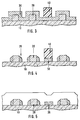
- FIGS. 1 to 4 represent purely schematic steps through successive manufacturing stages of semiconductor circuits. Identical features are provided with the same reference symbols in the figures.
- Printed conductors 20 made of metal, such as aluminum, or doped polysilicon (FIG. 1).
- the surface is then covered with a dielectric layer 30 of layer thickness d from e.g. SiO2 or phosphor silicate glass coated.
- the separation takes place e.g. by CVD (Fig. 2).
- a photoresist layer is now applied over the entire area and structured in a conventional manner to form the photomask 40, in such a way that it partially covers the layer 30 in the region between the conductor tracks 20.
- the minimum distance of the photomask 40 to the interconnects 20 is limited by technologically predetermined parameters such as layer thicknesses, adjustment accuracy of the exposure apparatus, optical properties of the tracks to be planarized, resolving power of the exposure machine for the photomask 40, etc. In practice, however, it is neither necessary nor desirable to work with minimum distances. Where the distances between conductor tracks 20 are too small, there is no photomask 40 (FIG. 3). These are areas in which the distance between the conductor tracks 20 is greater than a multiple of the thickness of the dielectric layer 30, and this includes the adjustment tolerances and the photo technology.
- the layer 30 is removed by anisotropic etching (FIG. 4).
- Spacers 35 remain on the edge of the conductor tracks 20, which represent a local planarization of the conductor track plane or correct undercut flanks of the conductor tracks 20, if necessary.
- the dielectric pieces 36 hidden under the photomask remain.
- the photomask 40 is removed and the planarization is continued in a conventional manner, so that the structure shown in FIG. 5 is obtained.
- a thin dielectric layer 31 can be applied for pre-planarization prior to the deposition of the dielectric layer 30 from e.g. Phosphorus silicate glass using the SOG method (not shown).
- a disadvantage of the method according to the invention is that an additional mask process has to be introduced. This contrasts with the fact that a reliable manufacturing process can only be feasible with this method. This applies in particular to circuits with non-periodic conductor track structures.
- this mask process is not critical if the additional dielectric pieces come sufficiently far from the structures to be leveled.
- the spacers on the conductor tracks created by the method contribute to the local planarization of the topography. They are part of the planarizations that are usually used.
Landscapes
- Internal Circuitry In Semiconductor Integrated Circuit Devices (AREA)
- Drying Of Semiconductors (AREA)
Applications Claiming Priority (2)
| Application Number | Priority Date | Filing Date | Title |
|---|---|---|---|
| DE4239075A DE4239075C1 (de) | 1992-11-20 | 1992-11-20 | Verfahren zur globalen Planarisierung von Oberflächen integrierter Halbleiterschaltungen |
| DE4239075 | 1992-11-20 |
Publications (2)
| Publication Number | Publication Date |
|---|---|
| EP0599074A1 true EP0599074A1 (fr) | 1994-06-01 |
| EP0599074B1 EP0599074B1 (fr) | 1999-04-21 |
Family
ID=6473289
Family Applications (1)
| Application Number | Title | Priority Date | Filing Date |
|---|---|---|---|
| EP93117463A Expired - Lifetime EP0599074B1 (fr) | 1992-11-20 | 1993-10-28 | Procédé de planarisation globale des surfaces de circuits intégrés semi-conducteurs |
Country Status (4)
| Country | Link |
|---|---|
| US (1) | US5445998A (fr) |
| EP (1) | EP0599074B1 (fr) |
| JP (1) | JPH076997A (fr) |
| DE (2) | DE4239075C1 (fr) |
Families Citing this family (7)
| Publication number | Priority date | Publication date | Assignee | Title |
|---|---|---|---|---|
| JP2926864B2 (ja) * | 1990-04-12 | 1999-07-28 | ソニー株式会社 | 銅系金属膜のエッチング方法 |
| US5840623A (en) * | 1995-10-04 | 1998-11-24 | Advanced Micro Devices, Inc. | Efficient and economical method of planarization of multilevel metallization structures in integrated circuits using CMP |
| JPH10112531A (ja) * | 1996-08-13 | 1998-04-28 | Hitachi Ltd | 半導体集積回路装置の製造方法 |
| KR100481981B1 (ko) * | 1997-12-29 | 2005-06-17 | 매그나칩 반도체 유한회사 | 반도체소자의층간절연막형성방법 |
| US6208004B1 (en) * | 1998-08-19 | 2001-03-27 | Philips Semiconductor, Inc. | Semiconductor device with high-temperature-stable gate electrode for sub-micron applications and fabrication thereof |
| US6448629B2 (en) | 1999-07-29 | 2002-09-10 | International Business Machines Corporation | Semiconductor device and method of making same |
| US7097788B2 (en) * | 2003-06-30 | 2006-08-29 | The Board Of Trustees Of The University Of Illinois | Conducting inks |
Citations (4)
| Publication number | Priority date | Publication date | Assignee | Title |
|---|---|---|---|---|
| EP0084635A2 (fr) * | 1981-12-30 | 1983-08-03 | International Business Machines Corporation | Procédé pour la formation d'une rainure large et profonde d'isolation remplie de diélectrique dans la surface rainure d'un substrat semi-conducteur en silicium |
| US4634496A (en) * | 1984-11-15 | 1987-01-06 | Kabushiki Kaisha Toshiba | Method for planarizing the surface of an interlayer insulating film in a semiconductor device |
| JPH0215624A (ja) * | 1988-03-24 | 1990-01-19 | Motorola Inc | 半導体デバイスの平坦化方法 |
| EP0405850A2 (fr) * | 1989-06-30 | 1991-01-02 | AT&T Corp. | Procédé de formation de diélectriques et composants ainsi produits |
Family Cites Families (8)
| Publication number | Priority date | Publication date | Assignee | Title |
|---|---|---|---|---|
| US4389281A (en) * | 1980-12-16 | 1983-06-21 | International Business Machines Corporation | Method of planarizing silicon dioxide in semiconductor devices |
| US4505029A (en) * | 1981-03-23 | 1985-03-19 | General Electric Company | Semiconductor device with built-up low resistance contact |
| US4662064A (en) * | 1985-08-05 | 1987-05-05 | Rca Corporation | Method of forming multi-level metallization |
| US4962060A (en) * | 1987-03-10 | 1990-10-09 | Advanced Micro Devices, Inc. | Making a high speed interconnect system with refractory non-dogbone contacts and an active electromigration suppression mechanism |
| GB2211348A (en) * | 1987-10-16 | 1989-06-28 | Philips Nv | A method of forming an interconnection between conductive levels |
| ATE115770T1 (de) * | 1989-09-08 | 1994-12-15 | Siemens Ag | Verfahren zur globalen planarisierung von oberflächen für integrierte halbleiterschaltungen. |
| US5229325A (en) * | 1991-01-31 | 1993-07-20 | Samsung Electronics Co., Ltd. | Method for forming metal wirings of semiconductor device |
| US5262352A (en) * | 1992-08-31 | 1993-11-16 | Motorola, Inc. | Method for forming an interconnection structure for conductive layers |
-
1992
- 1992-11-20 DE DE4239075A patent/DE4239075C1/de not_active Expired - Fee Related
-
1993
- 1993-10-28 DE DE59309525T patent/DE59309525D1/de not_active Expired - Fee Related
- 1993-10-28 EP EP93117463A patent/EP0599074B1/fr not_active Expired - Lifetime
- 1993-11-17 US US08/154,670 patent/US5445998A/en not_active Expired - Fee Related
- 1993-11-22 JP JP5292242A patent/JPH076997A/ja active Pending
Patent Citations (4)
| Publication number | Priority date | Publication date | Assignee | Title |
|---|---|---|---|---|
| EP0084635A2 (fr) * | 1981-12-30 | 1983-08-03 | International Business Machines Corporation | Procédé pour la formation d'une rainure large et profonde d'isolation remplie de diélectrique dans la surface rainure d'un substrat semi-conducteur en silicium |
| US4634496A (en) * | 1984-11-15 | 1987-01-06 | Kabushiki Kaisha Toshiba | Method for planarizing the surface of an interlayer insulating film in a semiconductor device |
| JPH0215624A (ja) * | 1988-03-24 | 1990-01-19 | Motorola Inc | 半導体デバイスの平坦化方法 |
| EP0405850A2 (fr) * | 1989-06-30 | 1991-01-02 | AT&T Corp. | Procédé de formation de diélectriques et composants ainsi produits |
Non-Patent Citations (1)
| Title |
|---|
| CHEMICAL PATENTS INDEX, DOCUMENTATION ABSTRACTS JOURNAL Section EI Week 9009, Derwent World Patents Index; Class U, AN 90-063004 * |
Also Published As
| Publication number | Publication date |
|---|---|
| DE59309525D1 (de) | 1999-05-27 |
| EP0599074B1 (fr) | 1999-04-21 |
| DE4239075C1 (de) | 1994-04-07 |
| US5445998A (en) | 1995-08-29 |
| JPH076997A (ja) | 1995-01-10 |
Similar Documents
| Publication | Publication Date | Title |
|---|---|---|
| DE68917995T2 (de) | Verfahren zum Herstellen einer Halbleitervorrichtung. | |
| DE3203898C2 (fr) | ||
| DE112009001476T5 (de) | Verfahren zum Herstellen von Halbleiterstrukturen und mittels solcher Verfahren erhaltene Halbleiterstrukturen | |
| DE10245179A1 (de) | Leitungen auf mehreren Ebenen mit reduziertem Rasterabstand | |
| DE102020008064A1 (de) | Tiefe grabenisolationsstruktur und verfahren zu deren herstellung | |
| DE102007026879A1 (de) | Verfahren zum Herstellen einer Struktur auf oder in einem Substrat, Abbildungsschicht zum Erzeugen sublithographischer Strukturen, Verfahren zum Invertieren eines sublithographischen Musters, durch Herstellung einer Struktur erhältliche Einrichtung | |
| DE69326269T2 (de) | Herstellungsverfahren von Kontaktöffnungen in integrierten Schaltungen | |
| DE68914099T2 (de) | Flankenabschrägen von Löchern durch dielektrische Schichten zur Erzeugung von Kontakten in integrierten Schaltkreisen. | |
| DE10154820B4 (de) | Verfahren zum Herstellen einer Maske für Halbleiterstrukturen | |
| EP0599074B1 (fr) | Procédé de planarisation globale des surfaces de circuits intégrés semi-conducteurs | |
| DE4232821C2 (de) | Verfahren zur Herstellung eines feinstrukturierten Halbleiterbauelements | |
| EP0105189B1 (fr) | Procédé de fabrication d'electrodes métalliques de différentes épaisseurs pour dispositifs à semi-conducteur en particulier pour des dispositifs à semi-conducteur de puissance comme des thyristors | |
| DE10259322B4 (de) | Verfahren zum Bilden einer Justiermarke in einer lichtundurchlässigen Schicht auf einem Substrat | |
| DE19719909A1 (de) | Zweifaches Damaszierverfahren | |
| DE10130824C2 (de) | Reparaturverfahren für einen dielektrischen Film mit einem Lochdefekt auf einem Substrat | |
| DE10200678A1 (de) | Verfahren zum Bearbeiten eines Substrats zum Ausbilden einer Struktur | |
| DE10239218A1 (de) | Verfahren zum Herstellen einer Halbleitervorrichtung und deren Aufbau | |
| DE3421127A1 (de) | Verfahren zum herstellen einer halbleiteranordnung | |
| EP0931439B1 (fr) | Technique pour constituer au moins deux niveaux de cablage sur des supports isoles electriquement | |
| DE19622415A1 (de) | CMOS-Halbleiterstruktur und Verfahren zur Herstellung derselben | |
| DE10312202B4 (de) | Verfahren zum Herstellen einer Ätzmaske auf einer Mikrostruktur, insbesondere einer Halbleiterstruktur mit Grabenkondensatoren, und entsprechende Verwendung der Ätzmaske | |
| DE2703473C2 (fr) | ||
| DE19935130C1 (de) | Verfahren zur Herstellung eines Kontaktloches für ein Halbleiterspeicherbauelement | |
| DE19927284C2 (de) | Verfahren zur Herstellung einer elektrisch leitfähigen Verbindung in einer mikroelektronischen Struktur | |
| EP0617463A1 (fr) | Procédé de fabrication d'un trou de contact |
Legal Events
| Date | Code | Title | Description |
|---|---|---|---|
| PUAI | Public reference made under article 153(3) epc to a published international application that has entered the european phase |
Free format text: ORIGINAL CODE: 0009012 |
|
| AK | Designated contracting states |
Kind code of ref document: A1 Designated state(s): DE FR NL |
|
| 17P | Request for examination filed |
Effective date: 19941130 |
|
| 17Q | First examination report despatched |
Effective date: 19960515 |
|
| RAP1 | Party data changed (applicant data changed or rights of an application transferred) |
Owner name: MICRONAS INTERMETALL GMBH |
|
| GRAG | Despatch of communication of intention to grant |
Free format text: ORIGINAL CODE: EPIDOS AGRA |
|
| GRAG | Despatch of communication of intention to grant |
Free format text: ORIGINAL CODE: EPIDOS AGRA |
|
| GRAH | Despatch of communication of intention to grant a patent |
Free format text: ORIGINAL CODE: EPIDOS IGRA |
|
| GRAH | Despatch of communication of intention to grant a patent |
Free format text: ORIGINAL CODE: EPIDOS IGRA |
|
| GRAA | (expected) grant |
Free format text: ORIGINAL CODE: 0009210 |
|
| AK | Designated contracting states |
Kind code of ref document: B1 Designated state(s): DE FR NL |
|
| REF | Corresponds to: |
Ref document number: 59309525 Country of ref document: DE Date of ref document: 19990527 |
|
| ET | Fr: translation filed | ||
| PLBE | No opposition filed within time limit |
Free format text: ORIGINAL CODE: 0009261 |
|
| STAA | Information on the status of an ep patent application or granted ep patent |
Free format text: STATUS: NO OPPOSITION FILED WITHIN TIME LIMIT |
|
| 26N | No opposition filed | ||
| PGFP | Annual fee paid to national office [announced via postgrant information from national office to epo] |
Ref country code: FR Payment date: 20011002 Year of fee payment: 9 |
|
| PGFP | Annual fee paid to national office [announced via postgrant information from national office to epo] |
Ref country code: DE Payment date: 20011004 Year of fee payment: 9 |
|
| PGFP | Annual fee paid to national office [announced via postgrant information from national office to epo] |
Ref country code: NL Payment date: 20011009 Year of fee payment: 9 |
|
| PG25 | Lapsed in a contracting state [announced via postgrant information from national office to epo] |
Ref country code: NL Free format text: LAPSE BECAUSE OF NON-PAYMENT OF DUE FEES Effective date: 20030501 Ref country code: DE Free format text: LAPSE BECAUSE OF NON-PAYMENT OF DUE FEES Effective date: 20030501 |
|
| PG25 | Lapsed in a contracting state [announced via postgrant information from national office to epo] |
Ref country code: FR Free format text: LAPSE BECAUSE OF NON-PAYMENT OF DUE FEES Effective date: 20030630 |
|
| NLV4 | Nl: lapsed or anulled due to non-payment of the annual fee |
Effective date: 20030501 |
|
| REG | Reference to a national code |
Ref country code: FR Ref legal event code: ST |