EP0599175B1 - Appareil d'interpolation pour une échelle graduée - Google Patents
Appareil d'interpolation pour une échelle graduée Download PDFInfo
- Publication number
- EP0599175B1 EP0599175B1 EP93118447A EP93118447A EP0599175B1 EP 0599175 B1 EP0599175 B1 EP 0599175B1 EP 93118447 A EP93118447 A EP 93118447A EP 93118447 A EP93118447 A EP 93118447A EP 0599175 B1 EP0599175 B1 EP 0599175B1
- Authority
- EP
- European Patent Office
- Prior art keywords
- signal
- input
- wave signal
- offset value
- value
- Prior art date
- Legal status (The legal status is an assumption and is not a legal conclusion. Google has not performed a legal analysis and makes no representation as to the accuracy of the status listed.)
- Expired - Lifetime
Links
Images


Classifications
-
- G—PHYSICS
- G01—MEASURING; TESTING
- G01D—MEASURING NOT SPECIALLY ADAPTED FOR A SPECIFIC VARIABLE; ARRANGEMENTS FOR MEASURING TWO OR MORE VARIABLES NOT COVERED IN A SINGLE OTHER SUBCLASS; TARIFF METERING APPARATUS; MEASURING OR TESTING NOT OTHERWISE PROVIDED FOR
- G01D5/00—Mechanical means for transferring the output of a sensing member; Means for converting the output of a sensing member to another variable where the form or nature of the sensing member does not constrain the means for converting; Transducers not specially adapted for a specific variable
- G01D5/12—Mechanical means for transferring the output of a sensing member; Means for converting the output of a sensing member to another variable where the form or nature of the sensing member does not constrain the means for converting; Transducers not specially adapted for a specific variable using electric or magnetic means
- G01D5/244—Mechanical means for transferring the output of a sensing member; Means for converting the output of a sensing member to another variable where the form or nature of the sensing member does not constrain the means for converting; Transducers not specially adapted for a specific variable using electric or magnetic means influencing characteristics of pulses or pulse trains; generating pulses or pulse trains
- G01D5/24471—Error correction
- G01D5/24476—Signal processing
-
- G—PHYSICS
- G01—MEASURING; TESTING
- G01D—MEASURING NOT SPECIALLY ADAPTED FOR A SPECIFIC VARIABLE; ARRANGEMENTS FOR MEASURING TWO OR MORE VARIABLES NOT COVERED IN A SINGLE OTHER SUBCLASS; TARIFF METERING APPARATUS; MEASURING OR TESTING NOT OTHERWISE PROVIDED FOR
- G01D5/00—Mechanical means for transferring the output of a sensing member; Means for converting the output of a sensing member to another variable where the form or nature of the sensing member does not constrain the means for converting; Transducers not specially adapted for a specific variable
- G01D5/12—Mechanical means for transferring the output of a sensing member; Means for converting the output of a sensing member to another variable where the form or nature of the sensing member does not constrain the means for converting; Transducers not specially adapted for a specific variable using electric or magnetic means
- G01D5/244—Mechanical means for transferring the output of a sensing member; Means for converting the output of a sensing member to another variable where the form or nature of the sensing member does not constrain the means for converting; Transducers not specially adapted for a specific variable using electric or magnetic means influencing characteristics of pulses or pulse trains; generating pulses or pulse trains
- G01D5/24471—Error correction
- G01D5/2448—Correction of gain, threshold, offset or phase control
Definitions
- the present invention relates to improvements in an interpolation device for a scale arrangement, and more particularly to an interpolation device for a scale arrangement which arrangement is used for detecting a rotational position of a motor, movement of a table in a machine tool and the like.
- a typical scale arrangement has a sensor such as a magnetic sensitive element which implements a readout of a scale in the form of an electrical signals of a sine wave and a cosine wave, and obtains the moving direction and position by analyzing the detected signals.
- a scale arrangement so as to keep a distance and an angle between a scale T and a sensor S constant during the operation of the scale arrangement.
- the sensor S generates a waving relative to the scale T as shown in Fig. 5, and the inclined angle of the sensor S relative to the scale T becomes different in the forward movement and the backward movement as shown in Fig. 6.
- Abbe's error occurs when the sensor S is not aligned parallel with the scale T in a non-contact type scale arrangement as shown in Fig. 7.
- a signal detected by the sensor S includes various errors.
- a DC offset voltage O A , O B is included in the signal as shown in Fig. 8; a deviation of a gain level is generated as shown in Fig.
- EP-A-0 377 045 discloses an encoder comprising first and second means for generating two sinusoidal scaling signals nominally 90° out of phase, first and second offset-correction means for the elimination of offset values in the first and second sinusoidal scaling signals, first and second amplitude correction means for the elimination of an amplitude difference in the first and second sinusoidal scaling signals, and first and second phase-correction means for adjusting the phase-difference between the first and second sinusoidal scaling signals to 90°.
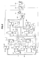
- FIG. 1 there is shown a first embodiment of an interpolation device for a scale arrangement.
- the input B is converted into a digital signal through an A/D converter within the sensor 1, and the converted signal is applied to one of two input terminals of the adder 3.
- the other input terminal of the adder 3 receives an average value (offset value) of an amplitude signal in a previous operation from an average circuit 5.
- a digital signal B1 from which an offset has been removed is outputted from the adder 3. Since the offset value is obtained as an average value between a maximum amplitude B max and a minimum amplitude B min as shown in Fig.
- the peak hold circuit 7 holds the maximum value Bmax of the input B according to a signal from a decision circuit 15.
- the peak hold circuit 9 holds a minimum value B min of the input B according to the signal from the decision circuit 15.
- the outputs from the peak hold circuits 7 and 9 are applied to the averaging circuit 5. In the averaging circuit 5, an average value is calculated as shown in the equation (3).
- the obtained average value is changed in polarization and then kept on.
- the output from the averaging circuit 5 is applied to an adder 11 wherein the output from the averaging circuit 5 is added with the maximum value B max from the peak hold circuit 7.
- the value B1 represented by the equation (4) and the value K B represented by the equation (5) are inputted into the divider 13, and a value B2 is obtained by dividing the equation (4) by the equation (5) and therefore represented as a normalized cosine wave by the following equation (6):
- B2 B1
- K B K B cos ⁇
- K B cos ⁇
- the input signal A is processed in the device shown in Fig. 1. That is, the input signal A is converted into a digital signal by an A/D converter of the sensor 2. Next, an offset value O A is subtracted from the converted digital signal through an adder 4. Further, a value A1 is normalized by the divider 14.
- Such translations are represented by the following equations (7), (8), (9) and (10):
- O A (A max + A min )/2
- A2 A1
- K A sin ( ⁇ + X)
- a function generator 22 generates a cosine wave signal cos( ⁇ ⁇ X) according to the output ⁇ ⁇ X from the adder 19.
- the polarity of the value X is determined according to the plus or minus character of cos( ⁇ +X).
- the inverse function generator 24 calculates tan ⁇ according to sin ⁇ from the function generator 23 and cos ⁇ from the divider 13, and outputs ⁇ which is an inverse function of tan ⁇ . With this operations in the interpolation device, a correct measured output ⁇ is obtained upon removing the phase drift during a detection by the sensor.
- one period of the periodical function is corresponding digital signals 0 to 199. Accordingly, when the sensor is moved in the forward direction (rightward in Fig. 12), the digital signal suddenly decreased from 199 to 0. When the sensor is moved in the backward direction (leftward in Fig. 12), the digital signal suddenly increases from 0 to 199. Accordingly, it is necessary to detect the moving direction of the sensor first.
- the latch circuit 67 keeps a previously measured signal and outputs it to the compactors 69 and 70.
- the previously measured signal is compared with predetermined values 20 and 180 in the comparators 69 and 70, respectively.
- the comparator 69 outputs a logical output 1 (high level) when the previous digital signal is larger than 180.
- the comparator 68 outputs a logical output 1 (low level) when the now digital signal is smaller than 20.
- Both outputs applies a logical input 1 to one of two input terminals of an AND circuit 81 through an AND circuit 75 and an OR circuit 83. This input is applied to a clock CK of a latch circuit 79, and the latch circuit 79 latches a new digital signal.
- a D flip-flop 77 is set according to the output of the comparator 69 such that the data in the forward direction is valid.
- the comparator 70 outputs an output 1 when the previous digital signal is smaller than 20.
- the comparator 71 outputs a logical output 1. Both outputs applies a logical input 1 to one of two input terminals of an AND circuit 82 through an AND circuit 73 and an OR circuit 84. This input is applied to a clock CK of a latch circuit 80 such that the latch circuit 80 latches a now digital signal.
- a D flip-flop 78 is set according to the output of the comparator 70 such that the data in the backward direction is valid. Since the output of a comparator 89 is 0 in both above-mentioned case, a clock input of a D flip-flop circuit is set at 0 (low level).
- the D flip-flop circuit 91 When the sensor is moving in the forward direction, an input A of the comparator 89 is increasing and at last a condition A ⁇ B is satisfied. In this situation, the clock input of the D flip-flop circuit 91 becomes 1 (high level), and the D flip-flop circuit 91 is set. Next, a D flip-flop circuit 92 is set, and a D flip-flop circuit 93 is set according to the output of the D flip-flop circuit 92. Accordingly, the D flip-flop circuit 93 outputs a decision output indicative that the sensor has moved one period (has passed a portion between digital signals 199 and 0). When the D flip-flop circuit 92 is turned on, the D flip-flop 77 is turned on. When the D flip-flop 92 is turned off by a next clock input, the D flip-flop 78 is turned on. Accordingly, the data in the both direction is treated to be valid, and the operation is repeated to a next period.
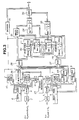
- Fig. 3 shows a second embodiment of the interpolation device of the scale arrangement.
- same numerals designate same parts and elements as that in Fig. 1, and the explanation thereof are facilitated herein.
- a divider 25 receives an output K B of an adder 11 and an output K A of an adder 12 and outputs an output K B / K A .
- a multiplier 26 receives a signal represented by the equation (8) from the adder 4 and a signal K B / K A from the divider 25 and outputs an output A2 which is represented by the following equation (12):
- an amplitude of a sine wave signal becomes the same as that of a cosine wave signal.
- A3 K B ⁇ sin ( ⁇ +X) - cos ⁇
- the equation (13) is modified as represented by the following equation (14):
- K' A 2K B sin ( ⁇ 4 - X 2 ) Since K A ' in the equation (15) indicates an amplitude, the peak hold circuit 30 holds the value represented by the equation (15).
- B3 K B ⁇ sin ( ⁇ + X) + cos ⁇
- Equation (16) is modified as represented by the following equation (17):
- K' B 2K B cos( ⁇ 4 - X 2 )
- the peak hold circuit 29 holds the value represented by the equation (18).
- a value represented by the following equation (19) is obtained.
- B4 A4 tan( ⁇ + ⁇ 4 + X 2 )
- the signal is a correct without phase lag X and used as a measured output.
- the signal is applied to a decision box 15 as mentioned above and used for generating a synchronizing signal. Accordingly, errors generated by the mechanical lag during the moving operation of the sensor is interpolated electrically, it is possible that the mechanical structure of the scale arrangement is formed simple.
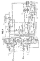
- FIG. 4 there is shown the interpolation device of the scale arrangement according to the present invention.
- same numerals designate same parts and elements as that in Fig. 3, and the explanation thereof are facilitated herein.
- a divider 32 output a signal represented by the equation (23) tan ( ⁇ / 4 + X / 2).
- the multiplier 38 outputs X which is twice the output of the adder 34.
- Function generators 39 and 40 generate signals sinX and cosX, respectively, by using the output of the multiplier 38.
- the plus-minus signal inversion of the signal sinX is transformed in the sign inversion circuit 41.
- the signal represented by the equation (34) is multiplied with an inverse number of cosX from the divider 42 in a multiplier 47, and a signal represented by the following equation (35) is outputted.
- an inverse function generator 24 On the basis of the signal represented by the equation (35) and the output of the adder 3, an inverse function generator 24 generates a signal represented by the following equation (36) and then outputs a signal represented by the following equation (37):
- B8 B1 ⁇
- the obtained signal ⁇ is a correct value without a phase drift and applied as a result of a measured signal.
Landscapes
- Physics & Mathematics (AREA)
- General Physics & Mathematics (AREA)
- Engineering & Computer Science (AREA)
- Signal Processing (AREA)
- Transmission And Conversion Of Sensor Element Output (AREA)
Claims (3)
- Appareil d'interpolation pour une échelle graduée, comprenant:caractérisé en ce que lesdits moyens de correction fournissent un signal représentant le produit (KB. SinΘ cosX) d'un signal de décalage représentant un état de décalage de phase entre le signal sinusoïdal provenant des premiers moyens de sortie et le signal cosinusoïdal provenant des seconds moyens de sortie, ainsi qu'un signal angulaire (KB. SinΘ) représentant un signal de mesure d'angle sur la base desdits signaux sinusoïdal et cosinusoïdal, les moyens de correction calculant de manière indépendante le signal de décalage représentant l'état de la phase de décalage et obtenant le signal d'angle mesuré correct en divisant (42, 47) ledit signal représentant le produit par le signal de décalage (cosX) obtenu de manière indépendante.des premiers moyens d'entrée (2) recevant de l'échelle graduée un signal d'entrée sous forme d'une onde sinusoïdale;des seconds moyens d'entrée (1) recevant de l'échelle graduée un signal d'entrée sous forme d'une onde cosinusoïdale;des premiers moyens de sortie comprenant un premier circuit de calcul de valeurs offset (4,6,8,10) calculant une valeur offset du signal d'entrée sinusoïdal et un premier circuit de calcul de coefficients d'amplitude (6,8,10,12) calculant un coefficient d'amplitude du signal d'entrée sinusoïdal, ces premiers moyens de sortie fournissant un signal sinusoïdal interpolé duquel la valeur offset de l'onde sinusoïdale d'entrée a été éliminée et qui présente un premier coefficient d'amplitude prédéterminé découlant des valeurs fournies par ledit premier circuit de calcul de valeurs offset et par ledit premier circuit de calcul de coefficients d'amplitude;des seconds moyens de sortie comprenant un second circuit de calcul de valeurs offset (3, 5, 7, 9) calculant une valeur offset du signal d'entrée cosinusoïdal et un second circuit de calcul de coefficients d'amplitude (5,7,9,11) calculant un coefficient d'amplitude du signal d'entrée cosinusoïdal, ces seconds moyens de sortie fournissant un signal cosinusoïdal duquel la valeur offset de l'onde cosinusoïdale a été éliminée et qui présente un second coefficient d'amplitude prédéterminé découlant des valeurs fournies par ledit second circuit de calcul de valeurs offset et par ledit second circuit de calcul de coefficients d'amplitude;des moyens de correction (42, 46, 47) corrigeant un décalage de phases entre ledit signal sinusoïdal fourni par lesdits premiers moyens de sortie et ledit signal cosinusoïdal fourni par lesdits seconds moyens de sortie, ces moyens de correction fournissant an angle mesuré correctement sur la base des signaux sinusoïdal et cosinusoïdal en décalage de phase corrigés; et par des moyens de décision (15) pour décider de l'accomplissement d'une période de la période de mesure sur la base du signal d'angle mesuré correct fourni par les moyens de correction et fournissant un signal de synchronisation auxdits premier et second moyens de sortie et aux moyens de correction,
- Appareil d'interpolation selon la revendication 1, caractérisé en ce que le circuit pour calculer la valeur offset comprend un circuit d'arrêt de valeurs maximum (7,8) pour maintenir une valeur maximum de l'amplitude du signal d'entrée et un circuit d'arrêt de valeurs minimum (9,10) pour maintenir une valeur minimum de l'amplitude du signal d'entrée, ledit circuit de calcul de valeurs offset calculant la valeur offset en formant une valeur moyenne entre la valeur maximum maintenue dans ledit circuit d'arrêt de valeurs maximum et la valeur minimum maintenue dans ledit circuit d'arrêt de valeurs minimum.
- Appareil d'interpolation selon l'une des revendications 1 ou 2, caractérisé en ce que le circuit de calcul du coefficient d'amplitude comprend un circuit (6,8,10,12; 5,7,9, 11) pour calculer l'amplitude du signal d'entrée comme la moitié d'une distance entre une valeur maximum et une valeur minimum de l'amplitude du signal d'entrée.
Applications Claiming Priority (2)
| Application Number | Priority Date | Filing Date | Title |
|---|---|---|---|
| JP4318181A JPH06167354A (ja) | 1992-11-27 | 1992-11-27 | スケールの内挿処理装置 |
| JP318181/92 | 1992-11-27 |
Publications (2)
| Publication Number | Publication Date |
|---|---|
| EP0599175A1 EP0599175A1 (fr) | 1994-06-01 |
| EP0599175B1 true EP0599175B1 (fr) | 1998-02-04 |
Family
ID=18096365
Family Applications (1)
| Application Number | Title | Priority Date | Filing Date |
|---|---|---|---|
| EP93118447A Expired - Lifetime EP0599175B1 (fr) | 1992-11-27 | 1993-11-15 | Appareil d'interpolation pour une échelle graduée |
Country Status (4)
| Country | Link |
|---|---|
| US (1) | US5485407A (fr) |
| EP (1) | EP0599175B1 (fr) |
| JP (1) | JPH06167354A (fr) |
| DE (1) | DE69316845T2 (fr) |
Cited By (1)
| Publication number | Priority date | Publication date | Assignee | Title |
|---|---|---|---|---|
| DE10034733B4 (de) * | 1999-08-02 | 2004-07-08 | Siemens Ag | Ermittlungsverfahren für ein Lagesignal und/oder für Korrekturwerte für Messsignale |
Families Citing this family (35)
| Publication number | Priority date | Publication date | Assignee | Title |
|---|---|---|---|---|
| DE4331151C2 (de) * | 1993-09-14 | 1997-05-22 | Baumueller Nuernberg Gmbh | System zur Messung der Absolutposition des beweglichen, zyklischen Teilungsmarken-Trägers eines inkrementalen Positionsgebers |
| JPH07218288A (ja) * | 1994-01-28 | 1995-08-18 | Mitsubishi Electric Corp | 絶対位置検出装置及びその誤差補正方法 |
| JPH08145719A (ja) * | 1994-09-22 | 1996-06-07 | Canon Inc | 位置または角度の検出方法 |
| JP3367226B2 (ja) * | 1994-10-20 | 2003-01-14 | ソニー・プレシジョン・テクノロジー株式会社 | 変位量検出装置 |
| DE19502276C2 (de) * | 1995-01-26 | 1999-12-09 | Gemac Ges Fuer Mikroelektronik | Interpolationsverfahren und hochauflösende digitale Interpolationseinrichtung |
| DE19544948C2 (de) * | 1995-12-01 | 2002-09-26 | Gemac Ges Fuer Mikroelektronik | Digitale Interpolationseinrichtung mit Amplituden- und Nullageregelung der Eingangssignale |
| JPH09264759A (ja) * | 1996-03-29 | 1997-10-07 | Mitsubishi Electric Corp | エンコーダの信号補正方法および装置 |
| JP3658094B2 (ja) * | 1996-07-26 | 2005-06-08 | キヤノン株式会社 | 電気内挿装置及びそれを用いた位置情報検出装置 |
| WO1998021553A1 (fr) | 1996-11-11 | 1998-05-22 | Fanuc Ltd. | Circuit d'interpolation de codeur |
| JP3026949B2 (ja) | 1997-05-12 | 2000-03-27 | ファナック株式会社 | エンコーダのオフセット補正回路 |
| DE50002537D1 (de) | 1999-03-30 | 2003-07-17 | Heidenhain Gmbh Dr Johannes | Verfahren und schaltungsanordnung zur korrektur von periodischen signalen eines inkrementalen positionsmesssystems |
| JP4154091B2 (ja) * | 1999-08-31 | 2008-09-24 | ソニーマニュファクチュアリングシステムズ株式会社 | 位置検出装置 |
| DE10056926A1 (de) | 2000-11-20 | 2002-07-18 | Optolab Licensing Gmbh | Verfahren und Vorrichtung zur Konditionierung eines periodischen Analogsignals |
| DE10124760A1 (de) * | 2001-05-21 | 2003-02-20 | Siemens Ag | Verfahren zur kontaktlosen, linearen Positionsmessung |
| US6518897B1 (en) * | 2001-08-29 | 2003-02-11 | Trw Inc. | Angle quantization using log division |
| EP1468496B1 (fr) * | 2002-01-11 | 2006-03-08 | Dr. Johannes Heidenhain GmbH | Procede d'interpolation d'au moins deux signaux analogiques dependants d'une position, periodiques, dephases l'un par rapport a l'autre |
| DE10301848B4 (de) * | 2003-01-09 | 2014-10-09 | Anton Rodi | Messeinrichtung zur Erfassung von Größen, insbesondere von Winkeln oder Wegstrecken |
| EP1471332A1 (fr) * | 2003-04-17 | 2004-10-27 | Dialog Semiconductor GmbH | Interface numérique pour un capteur de rotation |
| JP2004333156A (ja) | 2003-04-30 | 2004-11-25 | Harmonic Drive Syst Ind Co Ltd | エンコーダ信号内挿分割器 |
| JP4518786B2 (ja) * | 2003-12-12 | 2010-08-04 | 株式会社ミツトヨ | 内挿誤差補正方法及び装置 |
| JP2005208028A (ja) * | 2003-12-22 | 2005-08-04 | Minebea Co Ltd | バリアブルリラクタンスレゾルバ用角度演算方法とそのための角度演算装置 |
| GB0401748D0 (en) | 2004-01-27 | 2004-03-03 | Copley Motion Systems Llc | Linear motor and transducer arrangement therefor |
| EP1628123A1 (fr) | 2004-08-17 | 2006-02-22 | Dialog Semiconductor GmbH | Test de cameras miniaturisées avec fonctions de zoom optiques et/ou électroniques |
| JP4518871B2 (ja) * | 2004-08-24 | 2010-08-04 | 株式会社ミツトヨ | 内挿誤差補正方法及び装置 |
| US7933373B2 (en) * | 2006-06-19 | 2011-04-26 | Panasonic Corporation | Phase correction circuit of encoder signal |
| CN100535604C (zh) * | 2006-10-17 | 2009-09-02 | 财团法人工业技术研究院 | 电子细分割装置及其方法 |
| FR2902516A1 (fr) * | 2006-11-22 | 2007-12-21 | Siemens Vdo Automotive Sas | Dispositif et procede de conditionnement pour un capteur de position angulaire du type produisant au moins deux signaux periodiques dephases. |
| JP4943171B2 (ja) | 2007-01-30 | 2012-05-30 | 東芝機械株式会社 | 振幅検出装置 |
| JP5079346B2 (ja) | 2007-01-30 | 2012-11-21 | 東芝機械株式会社 | 波形補正装置および波形補正方法 |
| FI121202B (fi) * | 2007-03-14 | 2010-08-13 | Kone Corp | Laitteisto ja menetelmä kulman määrittämiseksi resolverilla |
| DE102008004916A1 (de) * | 2008-01-18 | 2009-07-23 | Conti Temic Microelectronic Gmbh | Verfahren zur Kalibrierung der Position eines Magnetfeldsensors |
| DE102009022084B4 (de) * | 2009-05-20 | 2015-07-09 | Sew-Eurodrive Gmbh & Co Kg | Verfahren zur Bestimmung der Winkelstellung eines drehbaren Teils |
| WO2011070391A1 (fr) * | 2009-12-10 | 2011-06-16 | Aktiebolaget Skf | Procédé d'estimation d'une position angulaire, dispositif de mesure et support de capteur |
| KR101418150B1 (ko) * | 2012-05-11 | 2014-08-07 | 한양대학교 산학협력단 | 정현파 광학 엔코더 신호 보상 방법 및 장치 |
| JP6732543B2 (ja) | 2016-06-02 | 2020-07-29 | Dmg森精機株式会社 | 変位検出装置 |
Family Cites Families (6)
| Publication number | Priority date | Publication date | Assignee | Title |
|---|---|---|---|---|
| US3831168A (en) * | 1973-06-06 | 1974-08-20 | Singer Co | Binary coded decimal-synchro converter |
| DE3024716C2 (de) * | 1980-06-30 | 1986-10-23 | Dr. Johannes Heidenhain Gmbh, 8225 Traunreut | Digitales Längen- oder Winkelmeßsystem |
| US4630033A (en) * | 1983-03-25 | 1986-12-16 | Hewlett-Packard Company | Method and apparatus for measuring phase |
| US4594540A (en) * | 1984-10-03 | 1986-06-10 | The United States Of America As Represented By The Administrator Of The National Aeronautics And Space Administration | Angular measurement system |
| JP2571096B2 (ja) * | 1988-04-18 | 1997-01-16 | ファナック株式会社 | エンコーダ |
| JP2501227B2 (ja) * | 1988-05-30 | 1996-05-29 | ファナック株式会社 | 絶対位置エンコ―ダ |
-
1992
- 1992-11-27 JP JP4318181A patent/JPH06167354A/ja active Pending
-
1993
- 1993-11-15 EP EP93118447A patent/EP0599175B1/fr not_active Expired - Lifetime
- 1993-11-15 DE DE69316845T patent/DE69316845T2/de not_active Expired - Fee Related
- 1993-11-16 US US08/152,390 patent/US5485407A/en not_active Expired - Fee Related
Cited By (1)
| Publication number | Priority date | Publication date | Assignee | Title |
|---|---|---|---|---|
| DE10034733B4 (de) * | 1999-08-02 | 2004-07-08 | Siemens Ag | Ermittlungsverfahren für ein Lagesignal und/oder für Korrekturwerte für Messsignale |
Also Published As
| Publication number | Publication date |
|---|---|
| US5485407A (en) | 1996-01-16 |
| DE69316845D1 (de) | 1998-03-12 |
| EP0599175A1 (fr) | 1994-06-01 |
| DE69316845T2 (de) | 1998-05-20 |
| JPH06167354A (ja) | 1994-06-14 |
Similar Documents
| Publication | Publication Date | Title |
|---|---|---|
| EP0599175B1 (fr) | Appareil d'interpolation pour une échelle graduée | |
| EP0772025B1 (fr) | Dispositif et procédé de détection de phase, pour un système de détection de position | |
| US7250881B2 (en) | Encoder output signal correction apparatus and method | |
| EP2209213B1 (fr) | Convertisseur RD et appareil de détection d'angle | |
| US7859254B2 (en) | Clock generation circuit, analog-digital angle converter using the same, and angle detection apparatus | |
| KR950014759B1 (ko) | 회전 펄스 인코더를 사용하여 극히 저속의 범위에서 전기 모터의 속도를 제어하기 위한 시스템 및 방법 | |
| US6522097B2 (en) | Position detecting apparatus and abnormality detecting apparatus | |
| JP3372450B2 (ja) | エンコーダの出力信号処理装置 | |
| EP0704679B1 (fr) | Appareil de détection de position | |
| EP1054238B1 (fr) | Procédé et appareil de détection de données positionelles utilisant de signaux décalés | |
| EP3957959A1 (fr) | Dispositif de détection d'angle | |
| JPH0658769A (ja) | 信号処理方法及びそれを用いた変位検出装置 | |
| US7443161B2 (en) | Method of determining angles | |
| KR100189937B1 (ko) | 정현파 신호를 사용한 회전각 추정 장치 및 방법 | |
| JPH0726858B2 (ja) | エンコーダ用信号処理回路 | |
| JPH0449892B2 (fr) | ||
| JP3439814B2 (ja) | デジタルpll装置 | |
| JPH05256638A (ja) | 誤差補正機能付き位置検出装置 | |
| JP3349575B2 (ja) | 変位速度検出方法および装置 | |
| JP3134707B2 (ja) | モータの位置および速度検出装置 | |
| JP2938472B2 (ja) | 回転角検出装置 | |
| JP3035835B2 (ja) | エンコーダ信号逓倍装置 | |
| JP3060122B2 (ja) | エンコーダ信号逓倍回路 | |
| JPH06160111A (ja) | 原点回路 | |
| JPH0777547A (ja) | 正弦波交流信号の周波数検出方法 |
Legal Events
| Date | Code | Title | Description |
|---|---|---|---|
| PUAI | Public reference made under article 153(3) epc to a published international application that has entered the european phase |
Free format text: ORIGINAL CODE: 0009012 |
|
| 17P | Request for examination filed |
Effective date: 19931115 |
|
| AK | Designated contracting states |
Kind code of ref document: A1 Designated state(s): CH DE GB LI NL |
|
| 17Q | First examination report despatched |
Effective date: 19940729 |
|
| GRAG | Despatch of communication of intention to grant |
Free format text: ORIGINAL CODE: EPIDOS AGRA |
|
| GRAG | Despatch of communication of intention to grant |
Free format text: ORIGINAL CODE: EPIDOS AGRA |
|
| GRAH | Despatch of communication of intention to grant a patent |
Free format text: ORIGINAL CODE: EPIDOS IGRA |
|
| RAP1 | Party data changed (applicant data changed or rights of an application transferred) |
Owner name: SONY PRECISION TECHNOLOGY INC. |
|
| GRAH | Despatch of communication of intention to grant a patent |
Free format text: ORIGINAL CODE: EPIDOS IGRA |
|
| GRAA | (expected) grant |
Free format text: ORIGINAL CODE: 0009210 |
|
| AK | Designated contracting states |
Kind code of ref document: B1 Designated state(s): CH DE GB LI NL |
|
| REG | Reference to a national code |
Ref country code: CH Ref legal event code: NV Representative=s name: PATENTANWALTSBUERO JEAN HUNZIKER Ref country code: CH Ref legal event code: EP |
|
| REF | Corresponds to: |
Ref document number: 69316845 Country of ref document: DE Date of ref document: 19980312 |
|
| PLBE | No opposition filed within time limit |
Free format text: ORIGINAL CODE: 0009261 |
|
| STAA | Information on the status of an ep patent application or granted ep patent |
Free format text: STATUS: NO OPPOSITION FILED WITHIN TIME LIMIT |
|
| 26N | No opposition filed | ||
| PGFP | Annual fee paid to national office [announced via postgrant information from national office to epo] |
Ref country code: GB Payment date: 19991020 Year of fee payment: 7 |
|
| PGFP | Annual fee paid to national office [announced via postgrant information from national office to epo] |
Ref country code: NL Payment date: 19991123 Year of fee payment: 7 |
|
| PGFP | Annual fee paid to national office [announced via postgrant information from national office to epo] |
Ref country code: CH Payment date: 19991129 Year of fee payment: 7 |
|
| PGFP | Annual fee paid to national office [announced via postgrant information from national office to epo] |
Ref country code: DE Payment date: 19991210 Year of fee payment: 7 |
|
| PG25 | Lapsed in a contracting state [announced via postgrant information from national office to epo] |
Ref country code: GB Free format text: LAPSE BECAUSE OF NON-PAYMENT OF DUE FEES Effective date: 20001115 |
|
| PG25 | Lapsed in a contracting state [announced via postgrant information from national office to epo] |
Ref country code: LI Free format text: LAPSE BECAUSE OF NON-PAYMENT OF DUE FEES Effective date: 20001130 Ref country code: CH Free format text: LAPSE BECAUSE OF NON-PAYMENT OF DUE FEES Effective date: 20001130 |
|
| PG25 | Lapsed in a contracting state [announced via postgrant information from national office to epo] |
Ref country code: NL Free format text: LAPSE BECAUSE OF NON-PAYMENT OF DUE FEES Effective date: 20010601 |
|
| GBPC | Gb: european patent ceased through non-payment of renewal fee |
Effective date: 20001115 |
|
| REG | Reference to a national code |
Ref country code: CH Ref legal event code: PL |
|
| NLV4 | Nl: lapsed or anulled due to non-payment of the annual fee |
Effective date: 20010601 |
|
| PG25 | Lapsed in a contracting state [announced via postgrant information from national office to epo] |
Ref country code: DE Free format text: LAPSE BECAUSE OF NON-PAYMENT OF DUE FEES Effective date: 20010801 |