EP0599290A1 - Gerät zum Extrahieren eines Synchronisierungssignals - Google Patents
Gerät zum Extrahieren eines Synchronisierungssignals Download PDFInfo
- Publication number
- EP0599290A1 EP0599290A1 EP93118924A EP93118924A EP0599290A1 EP 0599290 A1 EP0599290 A1 EP 0599290A1 EP 93118924 A EP93118924 A EP 93118924A EP 93118924 A EP93118924 A EP 93118924A EP 0599290 A1 EP0599290 A1 EP 0599290A1
- Authority
- EP
- European Patent Office
- Prior art keywords
- synchronizing signal
- output
- synchronizing
- circuit
- signal extracting
- Prior art date
- Legal status (The legal status is an assumption and is not a legal conclusion. Google has not performed a legal analysis and makes no representation as to the accuracy of the status listed.)
- Granted
Links
Images


Classifications
-
- H—ELECTRICITY
- H04—ELECTRIC COMMUNICATION TECHNIQUE
- H04L—TRANSMISSION OF DIGITAL INFORMATION, e.g. TELEGRAPHIC COMMUNICATION
- H04L7/00—Arrangements for synchronising receiver with transmitter
- H04L7/04—Speed or phase control by synchronisation signals
- H04L7/10—Arrangements for initial synchronisation
-
- G—PHYSICS
- G11—INFORMATION STORAGE
- G11B—INFORMATION STORAGE BASED ON RELATIVE MOVEMENT BETWEEN RECORD CARRIER AND TRANSDUCER
- G11B27/00—Editing; Indexing; Addressing; Timing or synchronising; Monitoring; Measuring tape travel
- G11B27/10—Indexing; Addressing; Timing or synchronising; Measuring tape travel
- G11B27/19—Indexing; Addressing; Timing or synchronising; Measuring tape travel by using information detectable on the record carrier
- G11B27/28—Indexing; Addressing; Timing or synchronising; Measuring tape travel by using information detectable on the record carrier by using information signals recorded by the same method as the main recording
- G11B27/30—Indexing; Addressing; Timing or synchronising; Measuring tape travel by using information detectable on the record carrier by using information signals recorded by the same method as the main recording on the same track as the main recording
- G11B27/3027—Indexing; Addressing; Timing or synchronising; Measuring tape travel by using information detectable on the record carrier by using information signals recorded by the same method as the main recording on the same track as the main recording used signal is digitally coded
-
- H—ELECTRICITY
- H04—ELECTRIC COMMUNICATION TECHNIQUE
- H04L—TRANSMISSION OF DIGITAL INFORMATION, e.g. TELEGRAPHIC COMMUNICATION
- H04L7/00—Arrangements for synchronising receiver with transmitter
- H04L7/04—Speed or phase control by synchronisation signals
- H04L7/08—Speed or phase control by synchronisation signals the synchronisation signals recurring cyclically
-
- H—ELECTRICITY
- H04—ELECTRIC COMMUNICATION TECHNIQUE
- H04L—TRANSMISSION OF DIGITAL INFORMATION, e.g. TELEGRAPHIC COMMUNICATION
- H04L7/00—Arrangements for synchronising receiver with transmitter
- H04L7/04—Speed or phase control by synchronisation signals
- H04L7/041—Speed or phase control by synchronisation signals using special codes as synchronising signal
- H04L7/042—Detectors therefor, e.g. correlators, state machines
Definitions
- the present invention relates to a synchronizing signal extracting apparatus for use in a digital signal recording/reproducing apparatus and the like.
- a digital audio tape recorder (DAT) and a digital video tape recorder (digital VTR) are known as digital signal recording/reproducing apparatuses.
- DAT digital audio tape recorder
- VTR digital video tape recorder
- a digitized video signal or audio signal is added with a synchronizing signal, an identification code, and an error correction code at each predetermined interval to form a sync block before being recorded.
- the synchronizing signal is detected to determine a head of the sync block to perform such processing as error correction and digital/analog conversion.
- the synchronizing signal is extracted only by means of matching patterns of one byte constituting the synchronizing signal and checking a simple parity.
- a synchronizing signal extracting apparatus for extracting a synchronizing signal from data reproduced from a digital VTR, comprising a synchronizing signal detecting circuit (a first circuit) for detecting the synchronizing signal having a predetermined number of bits from input digital data, a synchronizing signal generating circuit (a second circuit) constituted so that it can be reset by the first circuit and generates an output at a period of the synchronizing signal, and a synchronizing signal extracting circuit (a third circuit) which outputs as a synchronizing signal a result of an OR operation performed on the outputs of the first and second circuits and changes its state depending on a timing match or mismatch between the outputs of the first and second circuits.
- a synchronizing signal extracting apparatus in which the synchronizing signal extracting circuit outputs a signal for indicating validity of a synchronizing signal based on a state in which the circuit is operating.
- a synchronizing signal extracting apparatus in which the number of allowable bits at detection of a synchronizing signal is set according to the state of the synchronizing signal extracting circuit.
- a synchronizing signal extracting apparatus in which a synchronizing signal consists of two bytes, a detecting circuit (a fourth circuit) for detecting one byte of the synchronizing signal from input digital data is provided, and the two bytes of the synchronizing signal are detected by the synchronizing signal detecting circuit.
- the synchronizing signal generating circuit generates the output at the period of the synchronizing signal, so that, once the synchronizing signal detecting circuit has reset the synchronizing signal generating circuit upon detection of a synchronizing signal, the synchronizing signal is output from the synchronizing signal extracting circuit even if the synchronizing signal detecting circuit has missed detection of the synchronizing signal or made an erroneous detection thereof.
- the synchronizing signal extracting circuit outputs the signal for indicating the validity of the synchronizing signal to be output by this circuit according to the state of the circuit.
- This indicating signal goes high when, for example, the synchronizing signal detecting circuit detects one synchronizing signal and then detects a synchronizing signal in a timing that matches the output of the synchronizing signal generating circuit. This indicating signal goes low when two synchronizing signals are missed consecutively.
- the synchronizing signal detecting circuit detects one synchronizing signal at digital VTR variable-speed reproduction or high-speed search for example and then a synchronizing signal in a timing that matches the output of the synchronizing signal generating circuit, it is assumed that the synchronizing signal has been detected even if the synchronizing signal detecting circuit has not detected a complete match in synchronous pattern.
- the detecting circuit (the fourth circuit) detects one byte of the synchronizing signal and the synchronizing signal detecting circuit (the first circuit) detects two bytes of the synchronizing signal, thereby enhancing synchronizing signal detection accuracy.
- Fig. 1 is a block diagram illustrating a constitution of the synchronizing signal extracting apparatus practiced as a first embodiment of the invention.
- serial data entered at terminal 1 is divided in units of eight bits to be converted by a serial/parallel converting circuit 2 into eight-bit parallel data.
- the eight-bit parallel data thus obtained is entered in a first pattern matching circuit 3.
- the first pattern matching circuit 3 compares a pattern of a first one byte of a two-byte synchronizing signal and seven patterns generated by shifting the pattern of the first byte by one bit with a pattern of the entered eight-bit parallel data to determine by how many bits the first one byte of the synchronizing signal in the entered eight-bit parallel data has been offset in the eight-bit division.
- the first pattern matching circuit 3 then supplies a control signal corresponding to the offset to a barrel shifter 4 in which the eight-bit parallel signal is shifted to a normal alignment.
- the normally aligned parallel data is then entered in a second pattern matching circuit 5.
- the second pattern matching circuit 5 detects a match between patterns of the two bytes of the synchronizing signal in the entered data. Then the circuit 5 supplies a sync pulse SYNC1 to a state machine 8 in a timing in which the match has been detected.
- the circuit 5 also supplies a matching flag to a gate circuit 6.
- the gate circuit 6 opens when the state machine 8 is in search mode to supply the matching flag to a flywheel counter 7 to reset the counter.
- the flywheel counter 7 is a counter which operates in a period of one sync block and is reset by the output of the gate circuit 6 as described above. Then the counter 7 outputs a second sync pulse SYNC2.
- the state machine 8 performs an OR operation on the second sync pulse SYNC2 outputted from the flywheel counter 7 and the first sync pulse SYNC1 outputted from the pattern matching circuit 5 and outputs an operational result to a terminal 9 as a third sync pulse SYNC3.
- the state machine 8 outputs a D-EN signal (hereinafter referred to as a data enable signal) which indicates validity of the data from a terminal 10.
- the state machine 8 outputs a control signal for opening the gate circuit 6.
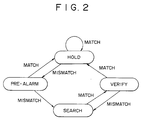
- the state machine 8 has four states; search, verify, hold and pre-alarm.
- Fig. 2 is a state transition diagram indicating an interrelation between these states.
- a pattern match is detected by the second pattern matching circuit 5.
- the state machine enters the verify mode. If no pattern match is found and the first sync pulse SYNC1 is not entered, the state machine stays in the search mode.
- the state machine 8 In the verify mode, if the second sync pulse SYNC2 outputted from the flywheel counter 7 and the first sync pulse SYNC1 outputted from the second pattern matching circuit 5 match in timing, the state machine 8 enters the hold mode. If no match is found, the state machine enters the search mode.
- the state machine 8 stays in the hold mode. If no match is found, the state machine shifts to the pre-alarm mode.
- the state machine 8 In the pre-alarm mode, if the second sync pulse SYNC2 and the first sync pulse SYNC1 match in timing, the state machine 8 enters the hold mode. If no match is found, the state machine shifts to the search mode.
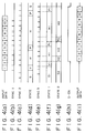
- Fig. 3 is a timing chart indicating an operation of the synchronizing signal extracting apparatus practiced as the first embodiment of the invention when no error is involved.
- Fig. 4 is a timing chart indicating an operation of the above-mentioned apparatus when an error is involved.
- Figs 1 through 3 the operation without error will be described.
- Fig. 3 (a) a situation in which two pieces of data each consisting of five sync blocks are entered intermittently is assumed in the following description.
- the input data is converted by the serial/parallel converter 2 into eight-bit parallel data.
- the resultant eight-bit parallel data is put in the first pattern matching circuit 3 and the barrel shifter 4.
- the parallel data is shifted to the normal alignment according to the offset of the synchronizing signal detected by the first pattern matching circuit 3.
- the normally aligned parallel data is then put in the second pattern matching circuit 5.
- the second pattern matching circuit 5 detects a match between the patterns of two bytes in the synchronizing signal in the entered parallel data and supplies the first sync pulse SYNC1 of Fig. 3 (b) to the state machine 8.
- the second pattern match circuit resets the flywheel counter 7.
- the flywheel counter 7 is reset in timings of the first sync pulse SYNC1 at first and sixth points shown in Fig. 3 (b).
- the state machine 8 exits the search mode (S) and enters the verify mode (V).
- the flywheel counter 7 outputs the second sync pulse SYNC2 of Fig. 3 (c).
- the flywheel counter 7 is reset by the output of the second pattern matching circuit 5
- the second sync pulse SYNC2 thereafter matches with the first sync pulse SYNC1 in timing.
- the state machine 8 performs an OR operation on the first sync pulse SYNC1 and the second sync pulse SYNC2 and outputs an operational result as a third sync pulse SYNC3.
- the operational result is output with a delay caused by processing in the state machine 8 (in the figure, the delay is 3/4 of sync block interval; actually, the delay is equivalent to several clocks).
- D-EN H2 + (H1 x V2) + (H1 x P2)
- H, V and P indicate the hold mode, the verify mode and the pre-alarm mode respectively.
- Numeral 1 indicates a state 1 in which, as shown in Fig. 3 (f), each mode in the state shown in Fig. 3 (d) is latched in a timing of the third sync pulse SYNC3.
- Numeral 2 indicates a state 2 in which, as shown in Fig. 3 (g), the state 1 of Fig. 3 (f) is delayed by one sync block.
- the data enable signal D-EN indicates that the third sync pulse SYNC3 which is output from the state machine 8 in this period is valid. As seen from Fig. 3 (h), the data enable signal D-EN goes high when the state machine 8 has entered the hold mode, or when one first sync pulse SYNC1 has been detected and then another first sync pulse SYNC1 has been detected in a timing matching that of the second sync pulse SYNC2. The data enable signal D-EN goes low when the state machine 8 has entered the search mode after passing through the pre-alarm mode, or when two first sync pulses SYNC1 have dropped consecutively. As shown in Fig. 3 (i), output data is delayed to match the timing of the data enable signal D-EN (delaying means is not shown).
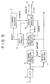
- Fig. 5 is a block diagram illustrating a constitution of the synchronizing signal extracting apparatus practiced as a second embodiment of the invention. It should be noted that those parts in Fig. 5 which are common with those in Fig. 1 are assigned with common reference numerals and are omitted from the following description.
- the second embodiment is characterized by that a state of the state machine 8 is supplied to the second matching circuit 5 and the number of allowable bits is set to determine a pattern match based on the supplied state.
- the state machine 8 when the state machine 8 is in the hold state, even if the two bytes or 16 bits do not all match in the second pattern matching circuit 5 and two to three bits do not match, a match is assumed and the second sync pulse SYNC2 is outputted.
- the state machine 8 is in the verify or pre-alarm mode, even if one bit of the 16 bits does not match, a match may be assumed to output the second sync pulse SYNC2.
- the second embodiment is effective especially when a signal-to-noise ratio of reproduced signal is poor at digital VTR variable-speed reproduction or high-speed search. That is, if the signal-to-noise ratio of reproduced signal is poor, the first embodiment may extremely degrade a frequency of occurrence of the first sync pulse SYNC1 in the second pattern matching circuit 5. Since the state machine 8 operates by comparing the first sync pulse SYNC1 with the second sync pulse SYNC2 which is outputted by the flywheel counter 7, if the first sync pulse does not come, the state machine 8 shifts to the search mode, eventually not outputting the data enable signal D-EN.
- the second embodiment is constituted such that the first sync pulse SYNC1 is generated even if an error is encountered, thereby overcoming the above-mentioned problem inherent to the first embodiment. Consequently, it is suitable to make control such that the setting of the digital VTR to variable-speed reproducing mode or high-speed search mode is detected by a microcomputer, not shown, and the state in which the state machine 8 is operating is supplied to the second pattern matching circuit 5.
- the present invention is not by any means limited to the above-mentioned embodiments and variations to it are possible as far as they are within the spirit of the invention.
- a synchronizing signal of one byte is detected in the first pattern matching circuit and a synchronizing signal of two bytes is detected in the second pattern matching circuit, these detecting operations may be performed only in the second pattern matching circuit.
- the novel setup outputs correct synchronizing signals and data enable signal even if the detection of synchronizing signals is missed or erroneously made, reduces chances of the missed detection of synchronizing signals even when the signal-to-noise ratio of reproduced signal is poor at digital VTR variable-speed reproduction or high-speed search, and implements synchronizing signal extraction of high precision.
Landscapes
- Engineering & Computer Science (AREA)
- Computer Networks & Wireless Communication (AREA)
- Signal Processing (AREA)
- Signal Processing For Digital Recording And Reproducing (AREA)
- Synchronisation In Digital Transmission Systems (AREA)
Applications Claiming Priority (3)
| Application Number | Priority Date | Filing Date | Title |
|---|---|---|---|
| JP33803592A JP3306938B2 (ja) | 1992-11-25 | 1992-11-25 | 同期符号抽出回路 |
| JP338035/92 | 1992-11-25 | ||
| JP33803592 | 1992-11-25 |
Publications (2)
| Publication Number | Publication Date |
|---|---|
| EP0599290A1 true EP0599290A1 (de) | 1994-06-01 |
| EP0599290B1 EP0599290B1 (de) | 2000-05-31 |
Family
ID=18314321
Family Applications (1)
| Application Number | Title | Priority Date | Filing Date |
|---|---|---|---|
| EP93118924A Expired - Lifetime EP0599290B1 (de) | 1992-11-25 | 1993-11-24 | Gerät zum Extrahieren eines Synchronisierungssignals |
Country Status (4)
| Country | Link |
|---|---|
| US (1) | US5523856A (de) |
| EP (1) | EP0599290B1 (de) |
| JP (1) | JP3306938B2 (de) |
| DE (1) | DE69328760T2 (de) |
Cited By (2)
| Publication number | Priority date | Publication date | Assignee | Title |
|---|---|---|---|---|
| EP0630016A3 (de) * | 1993-06-14 | 1995-08-23 | Ibm | Vorrichtung und Verfahren zur Erkennung eines Synchronisationszeichens in einem Datenaufzeichnungssystem. |
| EP1536423A4 (de) * | 2002-08-06 | 2006-04-05 | Sony Corp | Datentrugerwiedergabeeinrichtung und datentrugerwiedergabeverfahren |
Families Citing this family (6)
| Publication number | Priority date | Publication date | Assignee | Title |
|---|---|---|---|---|
| KR0127222B1 (ko) * | 1994-09-28 | 1998-04-03 | 구자홍 | 디지탈브이씨알의 식별코드 처리회로 |
| KR0147110B1 (ko) * | 1995-02-23 | 1998-10-15 | 구자홍 | 디브이씨알의 동기신호검출장치 |
| KR0148181B1 (ko) * | 1995-03-31 | 1998-10-15 | 김광호 | 디지탈 기록재생시스템의 가변적 동기패턴검출장치 및 방법 |
| US6098100A (en) * | 1998-06-08 | 2000-08-01 | Silicon Integrated Systems Corp. | Method and apparatus for detecting a wake packet issued by a network device to a sleeping node |
| US7012981B2 (en) * | 2001-04-17 | 2006-03-14 | Cyntrust Communications, Inc. | Method and apparatus for improving data frame synchronization in a low SNR environment |
| KR100721335B1 (ko) * | 2006-12-13 | 2007-05-25 | (주)이노스 | Tdd 시스템에 사용되는 동기추출회로 및 동기신호를추출하는 방법 |
Citations (8)
| Publication number | Priority date | Publication date | Assignee | Title |
|---|---|---|---|---|
| EP0052432A2 (de) * | 1980-11-18 | 1982-05-26 | Sony Corporation | Digitale Signalverarbeitung |
| EP0096854A2 (de) * | 1982-06-10 | 1983-12-28 | Nec Corporation | Rahmensynchronisierungssystem |
| EP0236017A2 (de) * | 1986-02-27 | 1987-09-09 | Sony Corporation | Dekodierung eines Synchronisationssignals |
| EP0254386A2 (de) * | 1986-04-18 | 1988-01-27 | Gpt Limited | Digitales Übertragungssystem |
| EP0443376A2 (de) * | 1990-02-22 | 1991-08-28 | Kabushiki Kaisha Toshiba | Rahmensynchronisierungsanordnung |
| EP0453876A2 (de) * | 1990-04-21 | 1991-10-30 | Alcatel SEL Aktiengesellschaft | Synchronisationsverfahren für SDH-Systeme sowie Verfahren und Schaltungsanordnung zum Erkennen unterschiedlicher Datenstrukturen |
| JPH04132431A (ja) * | 1990-09-25 | 1992-05-06 | Canon Inc | Resync検出回路 |
| JPH04134670A (ja) * | 1990-09-25 | 1992-05-08 | Olympus Optical Co Ltd | データ記録再生装置 |
Family Cites Families (10)
| Publication number | Priority date | Publication date | Assignee | Title |
|---|---|---|---|---|
| US4024571A (en) * | 1975-08-14 | 1977-05-17 | Rca Corporation | Synchronizing system employing burst crossover detection |
| JPS5485679A (en) * | 1977-12-20 | 1979-07-07 | Canon Inc | Wafer aligning unit |
| JPS5750021A (en) * | 1980-09-09 | 1982-03-24 | Victor Co Of Japan Ltd | Periodic signal detector |
| US4418364A (en) * | 1981-09-28 | 1983-11-29 | Rca Corporation | Video player apparatus having caption generator |
| US4639792A (en) * | 1982-10-21 | 1987-01-27 | The Stypher Corporation | Apparatus for decoding video address code signals |
| JPH0760574B2 (ja) * | 1984-03-26 | 1995-06-28 | 株式会社日立製作所 | 光デイスク装置のセクタ開始信号発生回路 |
| US4769704A (en) * | 1985-06-04 | 1988-09-06 | Matsushita Electric Industrial Co., Ltd. | Synchronization signal generator |
| DE3770283D1 (de) * | 1986-02-07 | 1991-07-04 | Sharp Kk | Optisches speichergeraet. |
| JPH02308424A (ja) * | 1989-05-24 | 1990-12-21 | Sony Corp | ピットパターンの検出方法 |
| US5229893A (en) * | 1989-05-31 | 1993-07-20 | Bts Broadcast Television Systems Gmbh | Circuit apparatus for deriving synchronizing pulses from playbacks of a video tape recording |
-
1992
- 1992-11-25 JP JP33803592A patent/JP3306938B2/ja not_active Expired - Fee Related
-
1993
- 1993-11-22 US US08/155,291 patent/US5523856A/en not_active Expired - Lifetime
- 1993-11-24 EP EP93118924A patent/EP0599290B1/de not_active Expired - Lifetime
- 1993-11-24 DE DE69328760T patent/DE69328760T2/de not_active Expired - Fee Related
Patent Citations (8)
| Publication number | Priority date | Publication date | Assignee | Title |
|---|---|---|---|---|
| EP0052432A2 (de) * | 1980-11-18 | 1982-05-26 | Sony Corporation | Digitale Signalverarbeitung |
| EP0096854A2 (de) * | 1982-06-10 | 1983-12-28 | Nec Corporation | Rahmensynchronisierungssystem |
| EP0236017A2 (de) * | 1986-02-27 | 1987-09-09 | Sony Corporation | Dekodierung eines Synchronisationssignals |
| EP0254386A2 (de) * | 1986-04-18 | 1988-01-27 | Gpt Limited | Digitales Übertragungssystem |
| EP0443376A2 (de) * | 1990-02-22 | 1991-08-28 | Kabushiki Kaisha Toshiba | Rahmensynchronisierungsanordnung |
| EP0453876A2 (de) * | 1990-04-21 | 1991-10-30 | Alcatel SEL Aktiengesellschaft | Synchronisationsverfahren für SDH-Systeme sowie Verfahren und Schaltungsanordnung zum Erkennen unterschiedlicher Datenstrukturen |
| JPH04132431A (ja) * | 1990-09-25 | 1992-05-06 | Canon Inc | Resync検出回路 |
| JPH04134670A (ja) * | 1990-09-25 | 1992-05-08 | Olympus Optical Co Ltd | データ記録再生装置 |
Non-Patent Citations (2)
| Title |
|---|
| PATENT ABSTRACTS OF JAPAN vol. 16, no. 401 (E - 1253) 25 August 1992 (1992-08-25) * |
| PATENT ABSTRACTS OF JAPAN vol. 16, no. 404 (P - 1410) 26 August 1992 (1992-08-26) * |
Cited By (3)
| Publication number | Priority date | Publication date | Assignee | Title |
|---|---|---|---|---|
| EP0630016A3 (de) * | 1993-06-14 | 1995-08-23 | Ibm | Vorrichtung und Verfahren zur Erkennung eines Synchronisationszeichens in einem Datenaufzeichnungssystem. |
| US5485476A (en) * | 1993-06-14 | 1996-01-16 | International Business Machines Corporation | Method and system for error tolerant synchronization character detection in a data storage system |
| EP1536423A4 (de) * | 2002-08-06 | 2006-04-05 | Sony Corp | Datentrugerwiedergabeeinrichtung und datentrugerwiedergabeverfahren |
Also Published As
| Publication number | Publication date |
|---|---|
| EP0599290B1 (de) | 2000-05-31 |
| JP3306938B2 (ja) | 2002-07-24 |
| DE69328760T2 (de) | 2000-12-28 |
| JPH06162669A (ja) | 1994-06-10 |
| DE69328760D1 (de) | 2000-07-06 |
| US5523856A (en) | 1996-06-04 |
Similar Documents
| Publication | Publication Date | Title |
|---|---|---|
| GB2038593A (en) | Apparatus for extracting a synchronizing signal | |
| US4777542A (en) | Data recording method | |
| EP0052432A2 (de) | Digitale Signalverarbeitung | |
| JP3366055B2 (ja) | 同期データ検出装置及び方法 | |
| US6272194B1 (en) | Synchronous signal detecting circuit, method, and information storage medium | |
| US4420775A (en) | Circuit and method for protecting a horizontal synchronous signal | |
| EP0146636B1 (de) | Synchronisierungsschaltung | |
| US5483538A (en) | Audio frame synchronization for embedded audio demultiplexers | |
| US5523856A (en) | Synchronizing signal detecting and error-correcting apparatus | |
| US5163070A (en) | Digital data synchronizer | |
| CA1214266A (en) | System for detecting a marker signal inserted in an information signal | |
| KR980700654A (ko) | 채널 신호를 정보 신호로 디코딩하는 장치 및 그 장치가 제공된 재생 장치(Apparatus for decoding a channel signal into an information signal and reproducing arrangement provided with the apparatus) | |
| JP2967649B2 (ja) | 受信同期回路 | |
| KR0154696B1 (ko) | 디지탈 기록 재생 장치의 동기 패턴 기록 및 검출회로 | |
| KR0141204B1 (ko) | 디지탈재생시스템의 동기신호검출장치 및 이를 구비한 데이타 변환장치 | |
| US5936922A (en) | Method and apparatus for sampling a synchronous pattern from data including an error using a random synchronous signal | |
| EP0856992B1 (de) | Datenwiedergabegerät zur Zeichenmultiplexierung eines Videosignals mit Taktfrequenzsynthese | |
| KR0148176B1 (ko) | 디지탈재생시스템의 데이타처리방법 및 장치 | |
| KR100209195B1 (ko) | 이상동기신호 방지장치 | |
| KR0186029B1 (ko) | 디지탈 데이타의 동기신호 제어회로 | |
| JP2982320B2 (ja) | 同期信号抽出回路 | |
| KR100195081B1 (ko) | 동기신호 처리회로 | |
| US20060002500A1 (en) | Method and apparatus for recovering a clock signal | |
| JPS6329343B2 (de) | ||
| JPH07169200A (ja) | ディジタル情報信号の再生装置 |
Legal Events
| Date | Code | Title | Description |
|---|---|---|---|
| PUAI | Public reference made under article 153(3) epc to a published international application that has entered the european phase |
Free format text: ORIGINAL CODE: 0009012 |
|
| AK | Designated contracting states |
Kind code of ref document: A1 Designated state(s): DE FR GB NL |
|
| 17P | Request for examination filed |
Effective date: 19941130 |
|
| 17Q | First examination report despatched |
Effective date: 19970711 |
|
| GRAG | Despatch of communication of intention to grant |
Free format text: ORIGINAL CODE: EPIDOS AGRA |
|
| GRAG | Despatch of communication of intention to grant |
Free format text: ORIGINAL CODE: EPIDOS AGRA |
|
| GRAH | Despatch of communication of intention to grant a patent |
Free format text: ORIGINAL CODE: EPIDOS IGRA |
|
| GRAH | Despatch of communication of intention to grant a patent |
Free format text: ORIGINAL CODE: EPIDOS IGRA |
|
| GRAA | (expected) grant |
Free format text: ORIGINAL CODE: 0009210 |
|
| AK | Designated contracting states |
Kind code of ref document: B1 Designated state(s): DE FR GB NL |
|
| REF | Corresponds to: |
Ref document number: 69328760 Country of ref document: DE Date of ref document: 20000706 |
|
| ET | Fr: translation filed | ||
| PLBE | No opposition filed within time limit |
Free format text: ORIGINAL CODE: 0009261 |
|
| STAA | Information on the status of an ep patent application or granted ep patent |
Free format text: STATUS: NO OPPOSITION FILED WITHIN TIME LIMIT |
|
| 26N | No opposition filed | ||
| REG | Reference to a national code |
Ref country code: GB Ref legal event code: IF02 |
|
| PGFP | Annual fee paid to national office [announced via postgrant information from national office to epo] |
Ref country code: NL Payment date: 20081103 Year of fee payment: 16 Ref country code: DE Payment date: 20081120 Year of fee payment: 16 |
|
| PGFP | Annual fee paid to national office [announced via postgrant information from national office to epo] |
Ref country code: FR Payment date: 20081112 Year of fee payment: 16 |
|
| PGFP | Annual fee paid to national office [announced via postgrant information from national office to epo] |
Ref country code: GB Payment date: 20081119 Year of fee payment: 16 |
|
| REG | Reference to a national code |
Ref country code: NL Ref legal event code: V1 Effective date: 20100601 |
|
| GBPC | Gb: european patent ceased through non-payment of renewal fee |
Effective date: 20091124 |
|
| REG | Reference to a national code |
Ref country code: FR Ref legal event code: ST Effective date: 20100730 |
|
| PG25 | Lapsed in a contracting state [announced via postgrant information from national office to epo] |
Ref country code: NL Free format text: LAPSE BECAUSE OF NON-PAYMENT OF DUE FEES Effective date: 20100601 Ref country code: FR Free format text: LAPSE BECAUSE OF NON-PAYMENT OF DUE FEES Effective date: 20091130 |
|
| PG25 | Lapsed in a contracting state [announced via postgrant information from national office to epo] |
Ref country code: DE Free format text: LAPSE BECAUSE OF NON-PAYMENT OF DUE FEES Effective date: 20100601 |
|
| PG25 | Lapsed in a contracting state [announced via postgrant information from national office to epo] |
Ref country code: GB Free format text: LAPSE BECAUSE OF NON-PAYMENT OF DUE FEES Effective date: 20091124 |