EP0599552A1 - Méthode et appareil électro-optique - Google Patents
Méthode et appareil électro-optique Download PDFInfo
- Publication number
- EP0599552A1 EP0599552A1 EP93309221A EP93309221A EP0599552A1 EP 0599552 A1 EP0599552 A1 EP 0599552A1 EP 93309221 A EP93309221 A EP 93309221A EP 93309221 A EP93309221 A EP 93309221A EP 0599552 A1 EP0599552 A1 EP 0599552A1
- Authority
- EP
- European Patent Office
- Prior art keywords
- optical
- signal
- interferometer
- signals
- electrodes
- Prior art date
- Legal status (The legal status is an assumption and is not a legal conclusion. Google has not performed a legal analysis and makes no representation as to the accuracy of the status listed.)
- Withdrawn
Links
Images




Classifications
-
- H—ELECTRICITY
- H04—ELECTRIC COMMUNICATION TECHNIQUE
- H04B—TRANSMISSION
- H04B10/00—Transmission systems employing electromagnetic waves other than radio-waves, e.g. infrared, visible or ultraviolet light, or employing corpuscular radiation, e.g. quantum communication
- H04B10/60—Receivers
-
- G—PHYSICS
- G02—OPTICS
- G02F—OPTICAL DEVICES OR ARRANGEMENTS FOR THE CONTROL OF LIGHT BY MODIFICATION OF THE OPTICAL PROPERTIES OF THE MEDIA OF THE ELEMENTS INVOLVED THEREIN; NON-LINEAR OPTICS; FREQUENCY-CHANGING OF LIGHT; OPTICAL LOGIC ELEMENTS; OPTICAL ANALOGUE/DIGITAL CONVERTERS
- G02F1/00—Devices or arrangements for the control of the intensity, colour, phase, polarisation or direction of light arriving from an independent light source, e.g. switching, gating or modulating; Non-linear optics
- G02F1/01—Devices or arrangements for the control of the intensity, colour, phase, polarisation or direction of light arriving from an independent light source, e.g. switching, gating or modulating; Non-linear optics for the control of the intensity, phase, polarisation or colour
- G02F1/21—Devices or arrangements for the control of the intensity, colour, phase, polarisation or direction of light arriving from an independent light source, e.g. switching, gating or modulating; Non-linear optics for the control of the intensity, phase, polarisation or colour by interference
- G02F1/225—Devices or arrangements for the control of the intensity, colour, phase, polarisation or direction of light arriving from an independent light source, e.g. switching, gating or modulating; Non-linear optics for the control of the intensity, phase, polarisation or colour by interference in an optical waveguide structure
-
- G—PHYSICS
- G02—OPTICS
- G02F—OPTICAL DEVICES OR ARRANGEMENTS FOR THE CONTROL OF LIGHT BY MODIFICATION OF THE OPTICAL PROPERTIES OF THE MEDIA OF THE ELEMENTS INVOLVED THEREIN; NON-LINEAR OPTICS; FREQUENCY-CHANGING OF LIGHT; OPTICAL LOGIC ELEMENTS; OPTICAL ANALOGUE/DIGITAL CONVERTERS
- G02F3/00—Optical logic elements; Optical bistable devices
-
- H—ELECTRICITY
- H03—ELECTRONIC CIRCUITRY
- H03K—PULSE TECHNIQUE
- H03K19/00—Logic circuits, i.e. having at least two inputs acting on one output; Inverting circuits
- H03K19/02—Logic circuits, i.e. having at least two inputs acting on one output; Inverting circuits using specified components
- H03K19/14—Logic circuits, i.e. having at least two inputs acting on one output; Inverting circuits using specified components using opto-electronic devices, i.e. light-emitting and photoelectric devices electrically- or optically-coupled
-
- H—ELECTRICITY
- H04—ELECTRIC COMMUNICATION TECHNIQUE
- H04L—TRANSMISSION OF DIGITAL INFORMATION, e.g. TELEGRAPHIC COMMUNICATION
- H04L25/00—Baseband systems
- H04L25/38—Synchronous or start-stop systems, e.g. for Baudot code
- H04L25/40—Transmitting circuits; Receiving circuits
- H04L25/49—Transmitting circuits; Receiving circuits using code conversion at the transmitter; using predistortion; using insertion of idle bits for obtaining a desired frequency spectrum; using three or more amplitude levels ; Baseband coding techniques specific to data transmission systems
- H04L25/4902—Pulse width modulation; Pulse position modulation
-
- H—ELECTRICITY
- H04—ELECTRIC COMMUNICATION TECHNIQUE
- H04L—TRANSMISSION OF DIGITAL INFORMATION, e.g. TELEGRAPHIC COMMUNICATION
- H04L25/00—Baseband systems
- H04L25/38—Synchronous or start-stop systems, e.g. for Baudot code
- H04L25/40—Transmitting circuits; Receiving circuits
- H04L25/49—Transmitting circuits; Receiving circuits using code conversion at the transmitter; using predistortion; using insertion of idle bits for obtaining a desired frequency spectrum; using three or more amplitude levels ; Baseband coding techniques specific to data transmission systems
- H04L25/493—Transmitting circuits; Receiving circuits using code conversion at the transmitter; using predistortion; using insertion of idle bits for obtaining a desired frequency spectrum; using three or more amplitude levels ; Baseband coding techniques specific to data transmission systems by transition coding, i.e. the time-position or direction of a transition being encoded before transmission
-
- G—PHYSICS
- G02—OPTICS
- G02F—OPTICAL DEVICES OR ARRANGEMENTS FOR THE CONTROL OF LIGHT BY MODIFICATION OF THE OPTICAL PROPERTIES OF THE MEDIA OF THE ELEMENTS INVOLVED THEREIN; NON-LINEAR OPTICS; FREQUENCY-CHANGING OF LIGHT; OPTICAL LOGIC ELEMENTS; OPTICAL ANALOGUE/DIGITAL CONVERTERS
- G02F1/00—Devices or arrangements for the control of the intensity, colour, phase, polarisation or direction of light arriving from an independent light source, e.g. switching, gating or modulating; Non-linear optics
- G02F1/01—Devices or arrangements for the control of the intensity, colour, phase, polarisation or direction of light arriving from an independent light source, e.g. switching, gating or modulating; Non-linear optics for the control of the intensity, phase, polarisation or colour
- G02F1/03—Devices or arrangements for the control of the intensity, colour, phase, polarisation or direction of light arriving from an independent light source, e.g. switching, gating or modulating; Non-linear optics for the control of the intensity, phase, polarisation or colour based on ceramics or electro-optical crystals, e.g. exhibiting Pockels effect or Kerr effect
- G02F1/0327—Operation of the cell; Circuit arrangements
-
- G—PHYSICS
- G02—OPTICS
- G02F—OPTICAL DEVICES OR ARRANGEMENTS FOR THE CONTROL OF LIGHT BY MODIFICATION OF THE OPTICAL PROPERTIES OF THE MEDIA OF THE ELEMENTS INVOLVED THEREIN; NON-LINEAR OPTICS; FREQUENCY-CHANGING OF LIGHT; OPTICAL LOGIC ELEMENTS; OPTICAL ANALOGUE/DIGITAL CONVERTERS
- G02F1/00—Devices or arrangements for the control of the intensity, colour, phase, polarisation or direction of light arriving from an independent light source, e.g. switching, gating or modulating; Non-linear optics
- G02F1/01—Devices or arrangements for the control of the intensity, colour, phase, polarisation or direction of light arriving from an independent light source, e.g. switching, gating or modulating; Non-linear optics for the control of the intensity, phase, polarisation or colour
- G02F1/21—Devices or arrangements for the control of the intensity, colour, phase, polarisation or direction of light arriving from an independent light source, e.g. switching, gating or modulating; Non-linear optics for the control of the intensity, phase, polarisation or colour by interference
- G02F1/212—Mach-Zehnder type
-
- G—PHYSICS
- G02—OPTICS
- G02F—OPTICAL DEVICES OR ARRANGEMENTS FOR THE CONTROL OF LIGHT BY MODIFICATION OF THE OPTICAL PROPERTIES OF THE MEDIA OF THE ELEMENTS INVOLVED THEREIN; NON-LINEAR OPTICS; FREQUENCY-CHANGING OF LIGHT; OPTICAL LOGIC ELEMENTS; OPTICAL ANALOGUE/DIGITAL CONVERTERS
- G02F2203/00—Function characteristic
- G02F2203/26—Pulse shaping; Apparatus or methods therefor
Definitions
- This invention relates to optical communications.
- Optical communications techniques are being used increasingly in commercial communications applications. Moreover, the designers of optical communication systems continue to focus on techniques for increasing the transmission capacity of such systems.
- the current state of the art is such that perchannel data rates in the 10-20 gigabit per second (Gbit/s) range have been demonstrated.
- the attainable data rates are limited principally by electrical signal processing considerations.
- electronic logic and other digital circuitry capable of operating at the highest rates that are attainable at any point in the evolution of the technology are typically not only expensive to design but are difficult to produce.
- technology capable of providing the highest attainable speed is typically not sufficiently mature to guarantee reliable long-term operation.
- the present invention provides a technique which can ameliorate the above-described problem in a variety of optical communications applications.
- at least two branches of an optical interferometer are controlled by respective time-varying electrical signals.
- those signals are other than substantially a) identical to, or b) in-phase inverses of each other.
- the constructive/destructive interference between the optical signals in the branches that results from using such signals to control the interferometer is such that, advantageously, any of a variety of functionalities are provided while eliminating at least some signal processing that heretofore had to be carried out in the electrical domain.
- electrical signals that would have had to have been processed at a desired output optical data rate can, by using the invention, be processed at a much lower, e.g., 50% lower rate, thereby ameliorating the electrical circuitry limitations described above.
- the invention may be used, for example, to multiplex N data signals, each having a data rate of B Gbit/s, to generate an optical signal encoded at N ⁇ B Gbit/s, the N data signals being applied with appropriate time-domain offsets to N control electrodes of the interferometer.
- the N constituent data signals are readily recovered from the output optical signal using only B Gbit/s logic circuitry.
- the invention may also be used, for example, to generate an optical signal which carries data, the value of which is a Boolean or other logic combination of the controlling electrical signals.
- encryption can be carried out by using a data signal at B Gbit/s as one of the controlling electrical signals and a signal representing a predetermined bit pattern at that same data bit rate as a second controlling electrical signal.
- the data rate of the output optical signal is also B Gbit/s.
- the two above-described or other functionalities can be carried out using a single interferometer by using a first set of electrodes to implement one of the functionalities, such as the multiplexing and using a second set of electrodes to implement the other one of the functionalities, such as the encryption.
- the electrodes of each set may be electrodes which control respective different branches of the interferometer or, in other embodiments may be electrodes which control a particular one branch of the interferometer. Combinations of these two approaches are also possible.
- the interferometer in carrying out the above and other functions implements an exclusive-OR/NOR functionality vis-a-vis the controlling electrical signals. That is, the constructive/destructive interference between the optical signals in the branches is such that the signals in the interferometer branches combine constructively (destructively) - thereby providing a first (second) optical output level - when the logic levels of an even (odd) number of the controlling electrical signals are "high".
- the optical output state can be negated by, for example, applying a constant offset signal to an electrode in order to induce a constant phase delay in the associated branch.
- an exclusive-OR function i.e., an exclusive-NOR function
- the invention could, if desired, be used strictly to provide at least some electrical-to-optical Boolean logic functions.
- a transmitter for multiplexing data signals to generate an optical signal in accordance with the principles of the invention is shown in FIG. 1.
- a laser diode 11 generates an optical return-to-zero (RZ) signal, which means that the optical power starts and ends at zero within each of a succession of signaling intervals (bit periods).
- the optical signal is applied via optical fiber 14 to interferometer 17.
- the output at the latter is applied to output optical fiber 18.
- the RZ signal is modulated by data signals provided from data source A, 21, and from data source B, 22.
- the data sources are clocked from a clock 15 at an illustrative clock rate of 5 GHz.
- the clock signal from clock 15 is also applied to laser driver/doubler 13 which drives laser diode 11 in such a way as to provide a 10 GHz RZ optical signal. That is, the optical signal from laser diode 11 is comprised of optical pulses which repeat at a 10 GHz rate.
- the output of data source 21 is applied to interferometer 17 via delay element 24 and bias-T 26.
- the output of data source 22 is applied to interferometer 17 via bias-T 23.
- bias-T23 an bias-T26 is to combine the signal levels of either one or both of the data signals with respective bias voltage signals, the purpose of which is explained at a more opportune point hereinbelow.
- delay element 24 is to adjust the relative phases of the data signals from the data sources 21, 22.
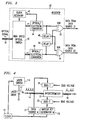
- FIG. 2 shows illustrative outputs of data sources A and B.
- the delay imparted by delay element 24 is adjusted to take into account any inherent phase difference between the outputs of the two data sources in such a way that the signal from data source A is delayed by half a bit period relative to the signal from data source B.
- Interferometer 17 multiplexes these two signals to form the exclusive-NOR function thereof.
- the optical output signal A ⁇ B ⁇ includes an optical pulse in each half-bit period for which the values of the two data signals are the same, i.e., both are "high” or both are “low”, and has no optical pulse in each half-bit period for which the values of the two data signals are different, i.e., one "high” and one "low".
- the output signals from the interferometer 17 are launched onto an optical fiber 18 to a remote location which can include a receiver 40.
- a receiver 40 Referring to FIG. 3 there is illustrated a receiver for receiving an optical signal that was launched on optical fiber 18.
- the components of the receiver shown in FIG. 3 are of conventional design and functionality and therefore only a brief discussion thereof is necessary.
- the 10 Gbit/s optical signal on fiber 18 is received by a high-speed optical switch 42 such as a lithium niobate directional switch operated by clock pulses from a clock recovery circuit 45 to direct the received pulses alternately to optical-to-electrical converters 44 and 46.
- a high-speed optical switch 42 such as a lithium niobate directional switch operated by clock pulses from a clock recovery circuit 45 to direct the received pulses alternately to optical-to-electrical converters 44 and 46.
- the optical-to-electrical converters 44, 46 operate at one half the optical transmission rate so that respective 5 Gbit/s electrical signals appear at the output of each, where the pulses in each signal represent the value of a particular pulse on fiber 18.
- the two output signals from the optical-to-electrical converters are phase-offset with respect to one another by T/2. This phase offset is compensated for by delay elements 48 and 50 in such a way that the bit which represents each optical pulse on fiber 18 is exclusive-ORed with the bit that represents the preceding optical pulse by one of exclusive-OR gates 52 or 54 and is exclusive-ORed with the bit that represents the succeeding optical pulse by the other one of those gates.
- the outputs of gates 52 and 54 are the recovered data signals from data sources A and B.
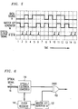
- FIG. 4 An alternative embodiment of a transmitter embodying the principles of the invention is shown in FIG. 4. Rather than multiplexing two 5 Gbit/s data signals to provide a 10 Gbit/s optical signal, this embodiment combines a single 5 Gbit/s data signal with a 5 Gbit/s fixed-bit-pattern signal, referred to as a "master key" signal, to provide a 5 Gbit/s encrypted optical signal.
- This embodiment is similar to that of FIG. 1 except that data source 22 is replaced by a master key generator 122 and the laser driver/doubler 13 is replaced with a laser driver 113 so that the optical pulses generated by laser diode 11 have a rate of 5 GHz. Additionally, delay element 24 is eliminated so that the outputs of data source 21 and master key generator 122 are phase-aligned. These two signals and the resulting optical output signal are shown in timing diagram FIG. 5.
- FIG. 6 An illustrative receiver for this embodiment is shown in FIG. 6.
- the optical signal on fiber 18 is converted to electrical form by optical-to-electrical converter 144 the output of which is applied to one input of exclusive-OR gate 152.
- the other input of gate 152 is provided by master key generator 132 which replicates the master key signal generated in the transmitter by master key generator 122. (The bit patterns generated by master key generators 122 and 132 are brought into synchronism in accordance with well-known techniques.)
- Master key generator 132 is clocked from clock recovery circuit 145 which recovers the transmit clock from converter 144.
- interferometer 17 is shown in FIG. 7.
- the interferometer is comprised of an electro-optic material substrate 200 such as lithium niobate (LiNbO3).
- An optical waveguide 222 is formed in the substrate via titanium (Ti) diffusion.
- the optical waveguide 222 is constructed to include two parallel branches 226, 228 positioned between two optical junctions 230, 232 which are coupled to two end waveguide sections 223,225.
- the ground plane and the electrodes can be electroplated onto the buffer layer and can be of aluminum, silver, gold or the like.
- One pair of electrodes can comprise an elongated electrode 236 positioned over optical waveguide 228 and a ground plane 240.
- the other pair of electrodes can comprise a ground plane 238 and an elongated electrode 234; the electrode 234 being positioned over optical waveguide 226.
- a common ground plane 233 can be included to cooperate with electrodes 234, 236.
- the assemblage of the LiNbO3 substrate, the optical Y junctions and associated optical waveguides, and a set of electrodes is one manifestation of an interferometer normally identified as a Y junction Mach-Zehnder interferometer.
- a change in the index of refraction of the waveguides - which is a function of the voltages applied to the single set of electrodes 234, 238; 236, 240 - causes an optical signal in the waveguides to experience an optical phase shift.
- the optical phase shift experienced by the optical signal in that branch is determined by the voltage applied to the electrodes associated with that branch.
- the optical energy received from laser diode 11 via optical fiber 14 is directed into end section 223 of waveguide 222 where it is divided into two equal optical signals by Y junction 230.
- the voltage levels representing Boolean levels "0" and "1" in the applied data signals are cause to be such that changing the value of one of those signals from one of the voltage levels to the other induces a phase shift of an odd number times ⁇ .
- the signals in branches 226, 228 combine constructively when the logic levels of the signals on electrodes 234, 236 are the same - thereby providing a first, maximum, optical output level - and combine destructively when the logic levels of the signals on electrodes 234, 236 are different - thereby providing a second, minimum, optical output level.
- the various operating parameters of the interferometer are initially adjusted in such a way that the maximum optical output is achieved when the signals on electrodes 234, 236 are both at their Boolean "0".
- FIG. 8 An alternative embodiment of an interferometer that can be used to realize the principles of the present invention is shown in FIG. 8.
- This interferometer is substantially identical to the interferometer in FIG. 7 except that a another set of electrodes 334, 338 and 336, 340 is provided for each of the two branches.
- Each of these pairs of electrodes induces an additional odd-number-of-half-wavelengths phase-shift when the logic level of the signal applied to it changes from a Boolean "0" to a Boolean "1".
- a signal to two of these pairs of electrodes or to more than two of the pairs of electrodes.
- a three-input exclusive-OR/NOR function - in which the output value depends on whether an odd or even number of inputs is "high" - can be realized by simply applying the third input to one of the pairs of electrodes 334, 338 or 336, 340.
- a four-input exclusive-OR/NOR function can be realized by applying the third and fourth inputs to respective ones of those sets.
- Another way in which the two sets of electrodes can be used is to use one set of electrodes to implement a first functionality, such as multiplexing and a second set to implement a second functionality such as encryption.
- any desired number of electrodes can be provided on any branch, as long as there are at least two sets of electrodes on the other branch.
- stability issues would have to be considered, one might be able to fabricate an interferometer having more than two branches.
- the optical signal input to the interferometer need not be a return-to-zero signal and the optical signal from the laser diode can be continuous-wave or of another form.
- the invention can also be used to generate an optical clock signal (steady stream of optical pulses).
- a continuous wave optical signal would be applied to the interferometer and an electrical clock signal would be used to supply both of the interferometer electrical input signals, which are delayed by an odd number quarter-periods.
- the frequency of the optical clock signal at the output of the interferometer would then have a frequency which is twice that of the electrical clock signal.
Landscapes
- Physics & Mathematics (AREA)
- Engineering & Computer Science (AREA)
- Nonlinear Science (AREA)
- Signal Processing (AREA)
- Computer Networks & Wireless Communication (AREA)
- Spectroscopy & Molecular Physics (AREA)
- General Physics & Mathematics (AREA)
- Optics & Photonics (AREA)
- Mathematical Physics (AREA)
- General Engineering & Computer Science (AREA)
- Computing Systems (AREA)
- Computer Hardware Design (AREA)
- Electromagnetism (AREA)
- Optical Communication System (AREA)
Applications Claiming Priority (2)
| Application Number | Priority Date | Filing Date | Title |
|---|---|---|---|
| US981955 | 1992-11-24 | ||
| US07/981,955 US5353114A (en) | 1992-11-24 | 1992-11-24 | Opto-electronic interferometic logic |
Publications (1)
| Publication Number | Publication Date |
|---|---|
| EP0599552A1 true EP0599552A1 (fr) | 1994-06-01 |
Family
ID=25528754
Family Applications (1)
| Application Number | Title | Priority Date | Filing Date |
|---|---|---|---|
| EP93309221A Withdrawn EP0599552A1 (fr) | 1992-11-24 | 1993-11-18 | Méthode et appareil électro-optique |
Country Status (3)
| Country | Link |
|---|---|
| US (1) | US5353114A (fr) |
| EP (1) | EP0599552A1 (fr) |
| JP (1) | JPH06202053A (fr) |
Cited By (3)
| Publication number | Priority date | Publication date | Assignee | Title |
|---|---|---|---|---|
| WO1996005605A1 (fr) * | 1994-08-15 | 1996-02-22 | Nigel Eric Rose | Ameliorations relatives a des systemes de commutation |
| WO2000070302A1 (fr) * | 1999-05-18 | 2000-11-23 | Campus Technologies Aktiengesellschaft | Dispositif d'acquisition ou de production de signaux optiques |
| FR2797331A1 (fr) * | 1999-08-03 | 2001-02-09 | Cit Alcatel | Differenciateur optique |
Families Citing this family (32)
| Publication number | Priority date | Publication date | Assignee | Title |
|---|---|---|---|---|
| US6674562B1 (en) | 1994-05-05 | 2004-01-06 | Iridigm Display Corporation | Interferometric modulation of radiation |
| US5524076A (en) * | 1994-01-28 | 1996-06-04 | Northern Telecom Limited | Chirp control of a Mach-Zehnder optical modulator using non-equal power splitting |
| US5566015A (en) * | 1994-03-09 | 1996-10-15 | International Business Machines Corporation | Optical demultiplexer with high speed superconducting switch |
| US7460291B2 (en) * | 1994-05-05 | 2008-12-02 | Idc, Llc | Separable modulator |
| US6680792B2 (en) | 1994-05-05 | 2004-01-20 | Iridigm Display Corporation | Interferometric modulation of radiation |
| US7138984B1 (en) | 2001-06-05 | 2006-11-21 | Idc, Llc | Directly laminated touch sensitive screen |
| US6188497B1 (en) | 1997-02-13 | 2001-02-13 | Lucent Technologies Inc. | Duo-binary signal encoding |
| US5917638A (en) * | 1997-02-13 | 1999-06-29 | Lucent Technologies, Inc. | Duo-binary signal encoding |
| US5831731A (en) * | 1997-02-24 | 1998-11-03 | Massachusetts Institute Of Technology | Apparatus and method for comparing optical bits |
| US5999284A (en) * | 1997-06-05 | 1999-12-07 | Northern Telecom Limited | Optical detection and logic devices with latching function |
| JP3179408B2 (ja) | 1998-04-06 | 2001-06-25 | 日本電気株式会社 | 導波路型光デバイス |
| US8928967B2 (en) | 1998-04-08 | 2015-01-06 | Qualcomm Mems Technologies, Inc. | Method and device for modulating light |
| WO1999052006A2 (fr) | 1998-04-08 | 1999-10-14 | Etalon, Inc. | Modulation interferometrique de rayonnement |
| US6763197B1 (en) * | 1999-06-08 | 2004-07-13 | Nippon Telegraph And Telephone Corporation | Optical transmitter and optical transmitter control method using variable duty ratio setting and alternate phase inversion for optical clock pulses |
| DE10009209A1 (de) * | 2000-02-26 | 2001-09-06 | Deutsche Telekom Ag | Vorrichtung zur Erzeugung, Addition und Subtraktion digitaler Folgen optischer Pulse und Verfahren zur sicheren Übertragung von Nachrichten |
| US6810407B1 (en) * | 2000-07-14 | 2004-10-26 | Lucent Technologies Inc. | Optical boolean logic devices for data encryption |
| US6522793B1 (en) | 2001-11-21 | 2003-02-18 | Andrei Szilagyi | Low voltage electro-optic modulator with integrated driver |
| US7369294B2 (en) | 2004-09-27 | 2008-05-06 | Idc, Llc | Ornamental display device |
| US7583429B2 (en) | 2004-09-27 | 2009-09-01 | Idc, Llc | Ornamental display device |
| US7535466B2 (en) | 2004-09-27 | 2009-05-19 | Idc, Llc | System with server based control of client device display features |
| US7808703B2 (en) | 2004-09-27 | 2010-10-05 | Qualcomm Mems Technologies, Inc. | System and method for implementation of interferometric modulator displays |
| US7586484B2 (en) | 2004-09-27 | 2009-09-08 | Idc, Llc | Controller and driver features for bi-stable display |
| US7920135B2 (en) | 2004-09-27 | 2011-04-05 | Qualcomm Mems Technologies, Inc. | Method and system for driving a bi-stable display |
| US7460246B2 (en) | 2004-09-27 | 2008-12-02 | Idc, Llc | Method and system for sensing light using interferometric elements |
| US7317568B2 (en) | 2004-09-27 | 2008-01-08 | Idc, Llc | System and method of implementation of interferometric modulators for display mirrors |
| US7653371B2 (en) | 2004-09-27 | 2010-01-26 | Qualcomm Mems Technologies, Inc. | Selectable capacitance circuit |
| US7916980B2 (en) | 2006-01-13 | 2011-03-29 | Qualcomm Mems Technologies, Inc. | Interconnect structure for MEMS device |
| US7582952B2 (en) | 2006-02-21 | 2009-09-01 | Qualcomm Mems Technologies, Inc. | Method for providing and removing discharging interconnect for chip-on-glass output leads and structures thereof |
| US7903047B2 (en) | 2006-04-17 | 2011-03-08 | Qualcomm Mems Technologies, Inc. | Mode indicator for interferometric modulator displays |
| US10397190B2 (en) * | 2016-02-05 | 2019-08-27 | Huawei Technologies Co., Ltd. | System and method for generating an obfuscated optical signal |
| US10207936B2 (en) | 2016-02-19 | 2019-02-19 | Silanna UV Technologies Pte Ltd | Ultraviolet reactor with planar light source |
| JP6860166B2 (ja) * | 2017-08-22 | 2021-04-14 | 日本電信電話株式会社 | 光演算器 |
Citations (1)
| Publication number | Priority date | Publication date | Assignee | Title |
|---|---|---|---|---|
| JPH03200923A (ja) * | 1989-12-28 | 1991-09-02 | Fujitsu Ltd | 光変調器 |
Family Cites Families (7)
| Publication number | Priority date | Publication date | Assignee | Title |
|---|---|---|---|---|
| US4878723A (en) * | 1986-02-06 | 1989-11-07 | Gte Laboratories Incorporated | Optically controlled semiconductor waveguide interferometer apparatus |
| US4763974A (en) * | 1987-08-13 | 1988-08-16 | Trw Inc. | Δβ-Phase reversal coupled waveguide interferometer |
| US5253309A (en) * | 1989-06-23 | 1993-10-12 | Harmonic Lightwaves, Inc. | Optical distribution of analog and digital signals using optical modulators with complementary outputs |
| US5034603A (en) * | 1989-11-06 | 1991-07-23 | Wilson Keith E | Integrated optics wavelength stabilization unit |
| DE58905184D1 (de) * | 1989-12-23 | 1993-09-09 | Heidenhain Gmbh Dr Johannes | Einrichtung mit wenigstens einem wellenleiterkoppler. |
| JPH04110831A (ja) * | 1990-08-31 | 1992-04-13 | Nec Corp | 光制御デバイス |
| US5214726A (en) * | 1991-10-07 | 1993-05-25 | United Technologies Corporation | Strain isolated integrated optic chip package |
-
1992
- 1992-11-24 US US07/981,955 patent/US5353114A/en not_active Expired - Lifetime
-
1993
- 1993-11-18 EP EP93309221A patent/EP0599552A1/fr not_active Withdrawn
- 1993-11-24 JP JP5292297A patent/JPH06202053A/ja not_active Withdrawn
Patent Citations (1)
| Publication number | Priority date | Publication date | Assignee | Title |
|---|---|---|---|---|
| JPH03200923A (ja) * | 1989-12-28 | 1991-09-02 | Fujitsu Ltd | 光変調器 |
Non-Patent Citations (3)
| Title |
|---|
| HANSEN P B ET AL: "A dual-drive Ti:LiNbO3 Mach-Zehnder modulator used as an optoelectronic logic gate for 10-Gb/s simultaneous multiplexing and modulation", IEEE PHOTONICS TECHNOLOGY LETTERS, vol. 4, no. 6, June 1992 (1992-06-01), NEW YORK US, pages 592 - 593, XP000275545 * |
| PATENT ABSTRACTS OF JAPAN vol. 015, no. 469 (P - 1281) 27 November 1991 (1991-11-27) * |
| TAYLOR H F: "Guided wave electrooptic devices for logic and computation", APPLIED OPTICS, vol. 17, no. 10, May 1978 (1978-05-01), NEW YORK US, pages 1493 - 1498 * |
Cited By (5)
| Publication number | Priority date | Publication date | Assignee | Title |
|---|---|---|---|---|
| WO1996005605A1 (fr) * | 1994-08-15 | 1996-02-22 | Nigel Eric Rose | Ameliorations relatives a des systemes de commutation |
| WO2000070302A1 (fr) * | 1999-05-18 | 2000-11-23 | Campus Technologies Aktiengesellschaft | Dispositif d'acquisition ou de production de signaux optiques |
| FR2797331A1 (fr) * | 1999-08-03 | 2001-02-09 | Cit Alcatel | Differenciateur optique |
| WO2001010045A3 (fr) * | 1999-08-03 | 2001-08-30 | Cit Alcatel | Differenciateur optique |
| US6628855B1 (en) | 1999-08-03 | 2003-09-30 | Alcatel | Optical differentiation device |
Also Published As
| Publication number | Publication date |
|---|---|
| US5353114A (en) | 1994-10-04 |
| JPH06202053A (ja) | 1994-07-22 |
Similar Documents
| Publication | Publication Date | Title |
|---|---|---|
| US5353114A (en) | Opto-electronic interferometic logic | |
| JP3268994B2 (ja) | デジタルデータの光学的伝送方法 | |
| US4965857A (en) | Method for synchronized polarization switching of an optical transmission signal of an optical transmission system having superheterodyne reception and an apparatus for the implementation of said method | |
| US6341031B1 (en) | Optical pulse generation using a high order function waveguide interferometer | |
| JPH10332939A (ja) | 光送信装置及び光送信方法 | |
| US5917642A (en) | Optical modulator | |
| US6917455B2 (en) | Cascaded RZ and NRZ laser modulators having RZ/NRZ phase alignment bias control | |
| EP1087256A2 (fr) | Modulateur optique | |
| US20040208642A1 (en) | Analog modulation of optical signals | |
| US20020114047A1 (en) | Cascaded RZ and NRZ laser modulators having RZ/NRZ phase alignment bias control | |
| US20030002118A1 (en) | Methods and apparatus for locking the phase between clock and data in return-to-zero modulation format | |
| US6940638B2 (en) | Optical frequency conversion systems and methods | |
| US20020141027A1 (en) | Variable pulse width optical pulse generation with superposed multiple frequency drive | |
| US7277645B2 (en) | High-bit-rate long-haul fiber optic communication system techniques and arrangements | |
| US7403711B2 (en) | Optical digital-to-analog converter and method of optically converting digital data to analog form | |
| US20020109893A1 (en) | Methods and apparatus for generating return-to-zero optically encoded data stream | |
| US6980746B2 (en) | Electronic RZ/CSRZ signal generation for optical communication systems | |
| TW200849856A (en) | Electrical generation of return-to-zero (RZ) data pattern with flexible duty cycle adjustment for optical transmission | |
| JP4809270B2 (ja) | 光送信装置及び方法 | |
| JP6900764B2 (ja) | 光送信機 | |
| US7450861B2 (en) | Return-to-zero alternative-mark-inversion optical transmitter and method for generating return-to-zero alternative-mark-inversion optical signal using the same | |
| JP2970776B2 (ja) | 光送信装置 | |
| JPH02167524A (ja) | 光送信装置 | |
| US4904963A (en) | Staggered quadrature phase shift keyed laser modulator | |
| EP1639729B1 (fr) | Emetteur pour signal de communication optique |
Legal Events
| Date | Code | Title | Description |
|---|---|---|---|
| PUAI | Public reference made under article 153(3) epc to a published international application that has entered the european phase |
Free format text: ORIGINAL CODE: 0009012 |
|
| AK | Designated contracting states |
Kind code of ref document: A1 Designated state(s): DE FR GB NL |
|
| RAP3 | Party data changed (applicant data changed or rights of an application transferred) |
Owner name: AT&T CORP. |
|
| 17P | Request for examination filed |
Effective date: 19941116 |
|
| 18W | Application withdrawn |
Withdrawal date: 19950314 |