JP6860166B2 - 光演算器 - Google Patents
光演算器 Download PDFInfo
- Publication number
- JP6860166B2 JP6860166B2 JP2017159096A JP2017159096A JP6860166B2 JP 6860166 B2 JP6860166 B2 JP 6860166B2 JP 2017159096 A JP2017159096 A JP 2017159096A JP 2017159096 A JP2017159096 A JP 2017159096A JP 6860166 B2 JP6860166 B2 JP 6860166B2
- Authority
- JP
- Japan
- Prior art keywords
- optical
- arithmetic
- signal
- input
- output
- Prior art date
- Legal status (The legal status is an assumption and is not a legal conclusion. Google has not performed a legal analysis and makes no representation as to the accuracy of the status listed.)
- Active
Links
Images


Landscapes
- Optical Modulation, Optical Deflection, Nonlinear Optics, Optical Demodulation, Optical Logic Elements (AREA)
Description

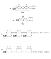
はじめに、本発明の実施の形態1における光演算器について、図1を参照して説明する。この光演算器は、カスケード接続された複数の演算部101を備える。演算部101は、入力信号に対して1つの光信号を出力するS個(Sは2以上の自然数)の演算素子102がシリアルに接続されて構成されている。演算部101は、S個の入力信号により1つの光信号を演算出力する。また、前段のS個の演算部101から出力された信号が、後段の1つの演算部101に入力される。なお、図1では、S=2の場合を例示している。また、図1では、カスケード接続の段数Mが3の場合を例示している。
次に、本発明の実施の形態2における光演算器について、図5を参照して説明する。なお、実施の形態2においても、図1を用いて説明したように、カスケード接続された複数の演算部101を備える。演算部101は、図5に示すように、入力される光信号に対して1つの光信号を出力するS個(Sは自然数)の演算素子102bがシリアルに接続されて構成されている。
次に、本発明の実施の形態3における光演算器について、図6を参照して説明する。実施の形態3では、多段にカスケード接続されたk=1段目の複数の演算部101aを、1入力1出力のマッハツェンダー干渉計から構成された演算素子102cと変換素子103cから構成している。マッハツェンダー干渉計の2つのアームに設けられた各々電気制御部に、入力信号X、入力信号Yが入力される。なお、k=2段目以降の演算部101は、前述した実施の形態1と同様の演算素子102と変換素子103から構成している。実施の形態3では、合成関数XNOR−ANDの演算を行う。
M=1のとき,S1=101,S2=103,F(10000,1)=(2125)τgate2,
M=2のとき,S1=100,S2=102,F(10000,2)=(550)τgate2,
M=3のとき,S1=100,S2=22,F(10000,3)=(541)τgate2,
M=4のとき,S1=100,S2=101,F(10000,4)=(640)τgate2,
M=1のとき,S1=100,S2=102,F(10000,1)=(325)τgate2,
M=2のとき,S1=100,S2=101,F(10000,2)=(370)τgate2。
次に、本発明の実施の形態4における光演算器について、図7を参照して説明する。実施の形態4では、多段にカスケード接続されたk=1段目の複数の演算部101aを、2入力2出力のマッハツェンダー干渉計を2段にシリアル接続した演算素子102dから構成している。この構成において、演算素子102dの前段のマッハツェンダー干渉計への電気制御入力をXiとし、後段のマッハツェンダー干渉計への電気制御入力をYiとする。なお、k=2段目以降の演算部101は、前述した実施の形態2と同様の演算素子102bと変換素子103bから構成している。実施の形態4では、合成関数XOR−ORの演算を行う。
Claims (5)
- 入力信号に対して1つの光信号を出力するS個(Sは2以上の自然数)の演算素子がシリアルに接続されて構成され、S個の前記入力信号により1つの光信号を演算出力する複数の演算部を備え、
前記複数の演算部は、カスケード接続され、
前段のS個の演算部から出力された信号が、後段の1つの演算部に入力される
ことを特徴とする光演算器。 - 請求項1記載の光演算器において、
前記入力信号は、電気信号であり、
前記複数の演算部の各々は、シリアル接続されている最終段の前記演算素子から出力された光信号を光電変換する変換素子を備える
ことを特徴とする光演算器。 - 請求項1記載の光演算器において、
前記入力信号は、光信号であり、
前記複数の演算部の各々は、S個の前記演算素子から光信号が出力された場合に値1を出力し、S個の前記演算素子から光信号が出力された場合以外に値0を出力する変換素子を備える
ことを特徴とする光演算器。 - 請求項2または3記載の光演算器において、
前記カスケード接続の段数Mおよび前記演算素子の個数Sは、前記入力信号の数Nと、前記演算素子における演算時間τgateと、前記変換素子における処理時間τOEOとから、S個の前記演算素子による演算遅延時間を示す(A)式が最小値となるときの実数値SとMを求め、求めた実数値SとMを自然数化し、自然数化した値を再度F(S)に代入してより小さな演算遅延時間を示すときのSとMとして決定されることを特徴とする光演算器。
- 請求項1記載の光演算器において、
1段目の前記複数の演算部は、前記演算素子がマッハツェンダー干渉計から構成され、
2段目以降の前記複数の演算部における前記演算素子は、電気信号である1つの前記入力信号に対して1つの光信号を出力する
ことを特徴とする光演算器。
Priority Applications (1)
| Application Number | Priority Date | Filing Date | Title |
|---|---|---|---|
| JP2017159096A JP6860166B2 (ja) | 2017-08-22 | 2017-08-22 | 光演算器 |
Applications Claiming Priority (1)
| Application Number | Priority Date | Filing Date | Title |
|---|---|---|---|
| JP2017159096A JP6860166B2 (ja) | 2017-08-22 | 2017-08-22 | 光演算器 |
Publications (2)
| Publication Number | Publication Date |
|---|---|
| JP2019039941A JP2019039941A (ja) | 2019-03-14 |
| JP6860166B2 true JP6860166B2 (ja) | 2021-04-14 |
Family
ID=65726420
Family Applications (1)
| Application Number | Title | Priority Date | Filing Date |
|---|---|---|---|
| JP2017159096A Active JP6860166B2 (ja) | 2017-08-22 | 2017-08-22 | 光演算器 |
Country Status (1)
| Country | Link |
|---|---|
| JP (1) | JP6860166B2 (ja) |
Families Citing this family (1)
| Publication number | Priority date | Publication date | Assignee | Title |
|---|---|---|---|---|
| WO2026078817A1 (en) * | 2024-10-09 | 2026-04-16 | Ntt, Inc. | Optical Circuit |
Family Cites Families (5)
| Publication number | Priority date | Publication date | Assignee | Title |
|---|---|---|---|---|
| JPH0648599B2 (ja) * | 1984-11-07 | 1994-06-22 | 日本電気株式会社 | 光シフトレジスタ回路 |
| US5353114A (en) * | 1992-11-24 | 1994-10-04 | At&T Bell Laboratories | Opto-electronic interferometic logic |
| JP2002174745A (ja) * | 2000-12-07 | 2002-06-21 | Kanagawa Acad Of Sci & Technol | 光集積回路およびその作製方法 |
| US20030112484A1 (en) * | 2001-12-03 | 2003-06-19 | Dmitry Ponomarenko | Optical multi-gate device and method |
| JP6707752B2 (ja) * | 2017-08-22 | 2020-06-10 | 日本電信電話株式会社 | 光乗算器および光乗算方法 |
-
2017
- 2017-08-22 JP JP2017159096A patent/JP6860166B2/ja active Active
Also Published As
| Publication number | Publication date |
|---|---|
| JP2019039941A (ja) | 2019-03-14 |
Similar Documents
| Publication | Publication Date | Title |
|---|---|---|
| Rahmani et al. | Application of nonlinear PhCRRs in realizing all optical half-adder | |
| US20190187380A1 (en) | Photon generator | |
| Peng et al. | Dnnara: A deep neural network accelerator using residue arithmetic and integrated photonics | |
| CN108702556A (zh) | 干涉仪和干涉仪设计方法 | |
| Ishihara et al. | An optical neural network architecture based on highly parallelized WDM-multiplier-accumulator | |
| CN117157617A (zh) | 用于执行算术运算的装置和方法 | |
| JP6860166B2 (ja) | 光演算器 | |
| JP6742584B2 (ja) | 光論理回路 | |
| CN102147634A (zh) | 基于单波导耦合微环谐振腔的光学向量-矩阵乘法器 | |
| Rakshit et al. | Design of micro ring resonator based all optical adder/subtractor | |
| Peng et al. | Integrated photonics architectures for residue number system computations | |
| Matsuo et al. | A synthesis method for power-efficient integrated optical logic circuits towards light speed processing | |
| Garai | Novel method of designing all optical frequency-encoded Fredkin and Toffoli logic gates using semiconductor optical amplifiers | |
| Deb et al. | Gates vs. splitters: Contradictory optimization objectives in the synthesis of optical circuits | |
| JP6707752B2 (ja) | 光乗算器および光乗算方法 | |
| Shiomi et al. | An integrated optical parallel multiplier exploiting approximate binary logarithms towards light speed data processing | |
| CN111240400A (zh) | 光除法模块、光子神经网络芯片、芯片系统及光除法器 | |
| Matsuo et al. | Methods for reducing power and area of BDD-based optical logic circuits | |
| Imai et al. | An optical parallel multiplier using nanophotonic analog adders and optoelectronic analog-to-digital converters | |
| CN106646756B (zh) | 一种基于光波导单侧耦合微腔阵列的全光开关 | |
| Kumar et al. | Realization of optical digital magnitude comparator using electro-optic effect based cascaded Mach-Zehnder interferometer structure | |
| Karempudi et al. | Design exploration and scalability analysis of a cmos-integrated, polymorphic, nanophotonic arithmetic-logic unit | |
| Pérez et al. | Reconfigurable lattice mesh designs for programmable photonic processors and universal couplers | |
| Saha et al. | A Survey on Optical Circuit Design | |
| Raju et al. | Modelling of 7-Segment Hex Decoder using Silicon Microring Resonator |
Legal Events
| Date | Code | Title | Description |
|---|---|---|---|
| A521 | Request for written amendment filed |
Free format text: JAPANESE INTERMEDIATE CODE: A821 Effective date: 20170822 |
|
| A621 | Written request for application examination |
Free format text: JAPANESE INTERMEDIATE CODE: A621 Effective date: 20190806 |
|
| A977 | Report on retrieval |
Free format text: JAPANESE INTERMEDIATE CODE: A971007 Effective date: 20200820 |
|
| A131 | Notification of reasons for refusal |
Free format text: JAPANESE INTERMEDIATE CODE: A131 Effective date: 20200908 |
|
| A601 | Written request for extension of time |
Free format text: JAPANESE INTERMEDIATE CODE: A601 Effective date: 20201109 |
|
| A521 | Request for written amendment filed |
Free format text: JAPANESE INTERMEDIATE CODE: A523 Effective date: 20201130 |
|
| TRDD | Decision of grant or rejection written | ||
| A01 | Written decision to grant a patent or to grant a registration (utility model) |
Free format text: JAPANESE INTERMEDIATE CODE: A01 Effective date: 20210316 |
|
| A61 | First payment of annual fees (during grant procedure) |
Free format text: JAPANESE INTERMEDIATE CODE: A61 Effective date: 20210318 |
|
| R150 | Certificate of patent or registration of utility model |
Ref document number: 6860166 Country of ref document: JP Free format text: JAPANESE INTERMEDIATE CODE: R150 |
|
| S111 | Request for change of ownership or part of ownership |
Free format text: JAPANESE INTERMEDIATE CODE: R313117 |
|
| R350 | Written notification of registration of transfer |
Free format text: JAPANESE INTERMEDIATE CODE: R350 |
|
| S533 | Written request for registration of change of name |
Free format text: JAPANESE INTERMEDIATE CODE: R313533 |
|
| R350 | Written notification of registration of transfer |
Free format text: JAPANESE INTERMEDIATE CODE: R350 |