EP0599739B1 - Thyristor und Aufbau von Thyristoren mit gemeinsamer Katode - Google Patents
Thyristor und Aufbau von Thyristoren mit gemeinsamer Katode Download PDFInfo
- Publication number
- EP0599739B1 EP0599739B1 EP93420413A EP93420413A EP0599739B1 EP 0599739 B1 EP0599739 B1 EP 0599739B1 EP 93420413 A EP93420413 A EP 93420413A EP 93420413 A EP93420413 A EP 93420413A EP 0599739 B1 EP0599739 B1 EP 0599739B1
- Authority
- EP
- European Patent Office
- Prior art keywords
- thyristor
- cathode
- region
- anode
- thyristors
- Prior art date
- Legal status (The legal status is an assumption and is not a legal conclusion. Google has not performed a legal analysis and makes no representation as to the accuracy of the status listed.)
- Expired - Lifetime
Links
Images

Classifications
-
- H—ELECTRICITY
- H10—SEMICONDUCTOR DEVICES; ELECTRIC SOLID-STATE DEVICES NOT OTHERWISE PROVIDED FOR
- H10D—INORGANIC ELECTRIC SEMICONDUCTOR DEVICES
- H10D64/00—Electrodes of devices having potential barriers
- H10D64/20—Electrodes characterised by their shapes, relative sizes or dispositions
- H10D64/27—Electrodes not carrying the current to be rectified, amplified, oscillated or switched, e.g. gates
- H10D64/291—Gate electrodes for thyristors
-
- H—ELECTRICITY
- H10—SEMICONDUCTOR DEVICES; ELECTRIC SOLID-STATE DEVICES NOT OTHERWISE PROVIDED FOR
- H10D—INORGANIC ELECTRIC SEMICONDUCTOR DEVICES
- H10D18/00—Thyristors
- H10D18/221—Thyristors having amplifying gate structures, e.g. cascade configurations
-
- H—ELECTRICITY
- H10—SEMICONDUCTOR DEVICES; ELECTRIC SOLID-STATE DEVICES NOT OTHERWISE PROVIDED FOR
- H10D—INORGANIC ELECTRIC SEMICONDUCTOR DEVICES
- H10D62/00—Semiconductor bodies, or regions thereof, of devices having potential barriers
- H10D62/10—Shapes, relative sizes or dispositions of the regions of the semiconductor bodies; Shapes of the semiconductor bodies
- H10D62/17—Semiconductor regions connected to electrodes not carrying current to be rectified, amplified or switched, e.g. channel regions
- H10D62/192—Base regions of thyristors
- H10D62/199—Anode base regions of thyristors
-
- H—ELECTRICITY
- H10—SEMICONDUCTOR DEVICES; ELECTRIC SOLID-STATE DEVICES NOT OTHERWISE PROVIDED FOR
- H10D—INORGANIC ELECTRIC SEMICONDUCTOR DEVICES
- H10D84/00—Integrated devices formed in or on semiconductor substrates that comprise only semiconducting layers, e.g. on Si wafers or on GaAs-on-Si wafers
- H10D84/60—Integrated devices formed in or on semiconductor substrates that comprise only semiconducting layers, e.g. on Si wafers or on GaAs-on-Si wafers characterised by the integration of at least one component covered by groups H10D10/00 or H10D18/00, e.g. integration of BJTs
Definitions
- the present invention relates to a thyristor structure and a monolithic assembly mode of thyristors at cathodes and common triggers, the triggers being referenced compared to cathodes.
- Figure 1 shows a very classic structure of thyristor.
- This structure is formed from an N2 substrate type N with a thickness of several hundred microns.
- a layer P P2 which corresponds to the anode of the thyristor coated with a metallization anode A.
- P2 P2
- P1 type P region corresponding to a trigger layer of cathode in which an N1 cathode region of type N.
- a metallization G is integral with the region of trigger and a metallization K is formed on the region N1 and forms the cathode electrode.
- N1 region interrupts which correspond to transmitter short circuits.
- thyristor At the periphery of the thyristor are formed from upper and lower faces of P 2 and 3 diffusions which are join to provide what is usually called a box thyristor structure.
- the trigger is referenced by compared to the cathode, i.e. the thyristor becomes conductor if, while its anode is positive with respect to its cathode, a positive voltage is applied between trigger and cathode to circulate a current from the trigger to the cathode.
- the thyristor manufacturers have long optimized doping levels and shapes seen from above layers and the shape of the short-circuit holes to optimize the various desired parameters of such cathode trigger thyristor, in particular its holding in voltage and its switching parameters on opening and the closure.
- FIG. 3 Another solution to get a trigger thyristor anode is illustrated in FIG. 3 in which the layer P1 of cathode trigger becomes an anode layer P2, the substrate N2 now has an anode trigger function, the layer P1 becomes a cathode trigger layer (not connected) and the cathode layer N1 is formed on the side of the lower face.
- the layer P1 of cathode trigger becomes an anode layer P2
- the substrate N2 now has an anode trigger function
- the layer P1 becomes a cathode trigger layer (not connected)
- the cathode layer N1 is formed on the side of the lower face.
- anode trigger thyristors Another disadvantage of anode trigger thyristors is that even if we knew how to make high-performance ones, they inherently have a trigger referenced to their anode whereas in many electrical assemblies, one wishes obtain thyristors whose triggering is obtained by a voltage referenced at the cathode and not at the anode. Another thyristor is described in GB-A-1580490.
- a first object of the invention is to realize a thyristor whose cathode corresponds to a first face main of a semiconductor chip (the underside) and whose trigger is on the face carrying the anode, while that the thyristor is triggered by a voltage applied to the trigger and referenced to the cathode.
- Another object of the present invention is to provide such a thyristor which is sensitive to closure, which exhibits a strong insensitivity to triggers in dv / dt and which can have a high value holding current.
- this invention provides a monolithic thyristor comprising a thyristor vertical comprising on the front face a localized anode region and on the rear side, a cathode metallization covering substantially all of this rear face, and, on the side of the face before, a lateral thyristor, whose anode and anode gate regions correspond to the anode and anode gate regions of the vertical thyristor.
- the thyristor trigger corresponds at the cathode or at the thyristor cathode trigger lateral; the cathode trigger region or the cathode, respectively, the lateral thyristor is connected to the cathode of the vertical thyristor.
- the invention provides a thyristor comprising an N-type substrate; on the front side, a region P-type anode coated with an anode metallization; on the back side, a layer P, in which a region is formed N of cathode, this rear face being coated with a metallization cathode, all of these layers forming a vertical thyristor; in the substrate, on the front faoe side, a box P in which an area N is formed, this box and this zone forming with the substrate and the anode region a lateral thyristor; an electrically connected trigger terminal to said box P or to said zone N; and an electrical connection between the cathode and said zone N or said box P, respectively.
- cathode region of vertical thyristor has short circuits emitter, and the cathode region of the lateral thyristor is free from transmitter short circuits.
- a P-type peripheral region goes from the upper face to the underside of the thyristor.
- this connection is ensured by metallization joining the cathode of the thyristor lateral and the upper surface of said peripheral region.
- the present invention also provides an assembly of common trigger thyristors and common cathodes made up the paralleling of thyristors as defined above, the cathodes of these thyristors being mounted on the same radiator.
- this assembly of thyristors with common triggers and cathodes sess is produced in monolithic form.
- Several thyristors verticals are assembled in parallel in the same substrate.
- This assembly includes additional regions cathode trigger cathode and thyristor cathode lateral which continues through the anode trigger regions and anode of each of the vertical thyristors.
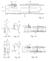
- Figure 4 shows a sectional view of a thyristor according to the present invention.
- This thyristor is developed from an N2 type N substrate with the back side coated a P1 type P layer in which an N1 region is formed type N cathode which can conventionally be interrupted to form regions of transmitter short circuits.
- the rear side is coated over substantially its entire surface with a cathode metallization.
- the N1 region is located opposite a region P2 formed from the upper face in the substrate N2.
- Region P2 constitutes the anode of a thyristor and is coated of an anode metallization A.
- region N2 is formed a P3 type P box inside which is formed an N3 type N region.
- the box P3 is integral with a metallization g and the N3 region of a metallization c.
- the thyristor of FIG. 4 presents opposite back a single cathode metallization and it's on the face before there is an anode metallization and metallizations additional g and c.
- a vertical thyristor TV comprising layers P2, N2, P1, N1 and a lateral thyristor tl, on the front side, comprising the layers N3, P3, N2, P2.
- the N1 region is conventionally provided with short circuits transmitter so that the main thyristor has a high IH and a high insensitivity to triggers in dV / dt.
- region N3 is not provided with transmitter short circuits so that the lateral thyristor is sensitive to closing.
- the structure of Figure 4 is susceptible to two mounting methods.
- terminal c is connected to terminal K and terminal g constitutes the trigger terminal G of the component.
- the operation of this first mounting method will be exposed in relation to the equivalent scheme in the form of layers of Figure 5B or equivalent diagram as Figure 5C circuit.
- the lateral thyristor P2-N2-P3-N3 and the vertical thyristor P2-N2-P1-N1 have in common their layers anode and anode trigger. Their cathodes N3 and N1 are connected. So when the voltage between terminals A and K is positive and a signal is applied to terminal G, the thyristor lateral P2-N2-P3-N3 becomes passing between terminals A and K. Immediately after, since a current flows between regions P2-N2, the vertical thyristor P2-N2-P1-N1 also becomes passing.
- the overall structure seen from terminals A, K and G (g) functions as a cathode gate thyristor in which the trigger is obtained by application of a positive trigger voltage with respect to cathode.
- An advantage of this structure in addition to the fact that it allows cathode mounting on a radiator, is that the parameters closing, i.e. sensitivity to current trigger are linked to the lateral thyristor tl while the parameters upon opening or parasitic triggering (HI and sensitivity in dV / dt) are related to the structure of the vertical thyristor TV. It is therefore possible to independently optimize these various settings.
- terminal g is connected to terminal K and terminal c constitutes the trigger terminal G of the component.
- the operation of this second mounting method will be exposed in relation to the equivalent scheme in the form of layers of Figure 6B or equivalent diagram as Figure 6C circuit.
- the lateral thyristor P2-N2-P3-N3 and the vertical thyristor P2-N2-P1-N1 have in common their layers anode and anode trigger.
- the cathode trigger layer of the lateral transistor is connected to the cathode K of the thyristor vertical.
- the lateral thyristor tl trips if its anode is positive with respect to its cathode and if the voltage on the terminal G (or c) is negative with respect to the voltage on terminal K. Then, as before, the vertical thyristor TV starts and the lateral thyristor tl is blocked.
- Figure 7 corresponds to an integrated embodiment of the assembly of FIG. 5A.
- the metallization of cathode c of lateral thyristor tl extends up to come into contact with P type lateral diffusion (2-3) joining layer P1 on the rear face.
- metallization c is not connected to a terminal external.
- FIG. 8 corresponds to an integrated embodiment of the assembly of FIG. 6A.
- the P3 region extends to come into contact with diffusion lateral 2-3 joining the rear face and metallization c corresponds to the control terminal G of the thyristor according to the invention.
- the thyristor according to the present invention can be used in isolation with the advantages indicated above, it finds a very particular application to circuits in which two (or more) thyristors are connected in cathodes and common triggers.
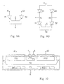
- Such a montage of two thyristors T1, T2 with K cathodes and common G triggers is illustrated in Figure 9A.
- These thyristors have anodes respectively designated by A1 and A2.
- This assembly is for example in certain controlled bridges as illustrated in FIG. 9B where an alternating voltage is supplied between the anodes A1 and A2.
- These anodes are connected to a first DC voltage terminal A via respective diodes D1 and D2 and the terminal K constitutes a second DC voltage terminal.
- FIG. 9B a single-phase circuit, we could likewise add a branch to constitute a three-phase circuit.
- thyristors T1 and T2 with cathodes common mounted on the same radiator we could use two thyristors according to the present invention in parallel. It is as possible as shown in Figure 10 to achieve a integrated structure in which we recognize right and left vertical thyristor structures, respectively P21-N2-P1-N11 and P22-N2-P1-N12, similar to that of FIG. 4 and in the central part the additional regions N3 and P3.
- the terminal c or terminal g can be connected to terminal K depending on whether you wish to carry out a control by trigger tension negative or positive with respect to the cathode. So when a control voltage is applied, that of thyristors T1 and T2 whose anode is positive with respect to the cathode will become driver.
- the doping levels of the various layers can for example be: layer N2 5.10 13 to 10 15 atoms / cm 3 , layer P1, regions P2 and P3 10 17 to 10 19 atoms / cm 3 , regions N1 and N3 10 20 to 10 21 atoms / cm 3 .
- the levels of doping of layers and regions P1, P2 and P3 are not necessarily identical and can be chosen different for optimize certain operating characteristics of the thyristor.
- the structure has been presented according to the invention as formed from a substrate N thick (a few hundred micrometers) in which are formed by diffusion or implantation of the other layers or regions.
- a substrate N thick (a few hundred micrometers) in which are formed by diffusion or implantation of the other layers or regions.
- any known method of manufacturing thyristors can be used. We could for example start from a substrate of type P corresponding to the region P1 on which the layer N2 is caused to grow by epitaxy.
Landscapes
- Thyristors (AREA)
Claims (8)
- Monolitische Thyristor, welcher einen Vertikalthyristor (TV) umfaßt, der auf der Vorderseite einen lokalisierten Anodenbereich (P2) und auf der Rückseite eine Kathodenmetallisierung (K) aufweist, welche im wesentlichen diese gesamte Rückseite bedeckt, dadurch gekennzeichnet, daß:der Thyristor des weiteren an der Vorderseite einen Lateralthyristor (tl) aufweist, dessen Anodenbereich und Anoden-Gate-Bereich dem Anodenbereich und dem Anoden-Gate-Bereich des Vertikalthyristors entsprechen,das Gate des Thyristors der Kathode (c) oder dem Kathoden-Gate (g) des Lateralthyristors entspricht, unddas Kathoden-Gate (g) bzw. die Kathode (c) des Lateralthyristors mit der Kathode des Vertikalthyristors verbunden ist.
- Thyristor nach Anspruch 1, welcher umfaßt:dadurch gekennzeichnet, daß der Thyristor des weiteren umfaßt:ein N-Substrat (N2);auf der Vorderseite einen mit einer Anodenmetallisierung überzogenen Anodenbereich vom P-Typ (P2);auf der Rückseite eine P-Schicht (P1), in welcher ein N-Kathodenbereich (N1) ausgebildet ist, wobei diese Rückseite mit einer Kathodenmetallisierung überzogen ist und diese Schichten insgesamt einen Vertikalthyristor (TV) bilden;in dem Substrat an der Vorderseite einen P-Graben bzw. -Schacht (P3), in welchem eine N-Zone (N3) ausgebildet ist, wobei dieser Graben bzw. Schacht und diese Zone mit dem Substrat (N2) und dem Anodenbereich (P2) einen Lateralthyristor (tl) bilden;einen elektrisch mit dem genannten P-Graben bzw. -Schacht oder mit der genannten N-Zone verbundenen Gate-Anschluß (G); sowieeine elektrische Verbindung zwischen der Kathode und der genannten N-Zone bzw. dem genannten P-Graben bzw. -Schacht.
- Thyristor nach Anspruch 1 oder 2,
dadurch gekennzeichnet, daß der Kathodenbereich (N1) des Vertikalthyristors (TV) mit Emitter-Kurzschlüssen versehen ist und daß der Kathodenbereich (N3) des Lateralthyristors frei von Emitter-Kurzschlüssen ist. - Thyristor nach einem der Ansprüche 1 bis 3,
dadurch gekennzeichnet, daß er einen Umfangsbereich vom P-Typ (2, 3) aufweist, der sich von seiner Ober- bzw. Vorderseite bis zu seiner Rück- bzw. Unterseite erstreckt. - Thyristor nach Anspruch 4, mit einer Verbindung zwischen dem Kathoden-Gate-Bereich (P3) des Lateralthyristors und der Kathodenmetallisierung,
dadurch gekennzeichnet, daß die genannte Verbindung durch eine Kontinuität zwischen dem genannten Gate-Bereich (P3) und dem genannten Umfangsbereich gebildet wird. - Thyristor nach Anspruch 4, mit einer Verbindung zwischen dem Kathodenbereich (N3) des Lateralthyristors und der Kathodenmetallisierung,
dadurch gekennzeichnet, daß die genannte Verbindung durch eine die Kathode des Lateralthyristors und die Oberseite des genannten Umfangsbereichs verbindende Metallisierung gewährleistet wird. - Thyristoranordnung mit gemeinsamen Gates und gemeinsamen Kathoden,
dadurch gekennzeichnet, daß sie aus einer Parallelanordnung von Thyristoren gemäß einem der Ansprüche 1 bis 6 besteht, wobei die Kathoden dieser Thyristoren auf ein und demselben Kühlkörper montiert sind. - Thyristoranordnung mit gemeinsamen Gates und gemeinsamen Kathoden in monolithischer Ausbildung,
dadurch gekennzeichnet, daß die mehreren Vertikalthyristoren gemäß einem der Ansprüche 1 bis 6 in ein und demselben Substrat parallel zueinander angeordnet sind und daß die Anordnung zusätzliche gemeinsame Kathoden-Gate-Bereiche und Kathodenbereiche eines Lateralthyristors umfaßt, die sich jeweils in die Anoden-Gate-Bereiche und Anodenbereiche jedes der Vertikalthyristoren fortsetzen.
Applications Claiming Priority (2)
| Application Number | Priority Date | Filing Date | Title |
|---|---|---|---|
| FR9213340A FR2697674B1 (fr) | 1992-10-29 | 1992-10-29 | Thyristor et assemblage de thyristors à cathode commune. |
| FR9213340 | 1992-10-29 |
Publications (2)
| Publication Number | Publication Date |
|---|---|
| EP0599739A1 EP0599739A1 (de) | 1994-06-01 |
| EP0599739B1 true EP0599739B1 (de) | 1999-12-22 |
Family
ID=9435267
Family Applications (1)
| Application Number | Title | Priority Date | Filing Date |
|---|---|---|---|
| EP93420413A Expired - Lifetime EP0599739B1 (de) | 1992-10-29 | 1993-10-25 | Thyristor und Aufbau von Thyristoren mit gemeinsamer Katode |
Country Status (5)
| Country | Link |
|---|---|
| US (1) | US5365086A (de) |
| EP (1) | EP0599739B1 (de) |
| JP (1) | JP3635098B2 (de) |
| DE (1) | DE69327388T2 (de) |
| FR (1) | FR2697674B1 (de) |
Families Citing this family (9)
| Publication number | Priority date | Publication date | Assignee | Title |
|---|---|---|---|---|
| WO1995034914A1 (en) * | 1994-06-10 | 1995-12-21 | Beacon Light Products, Inc. | High temperature, high holding current semiconductor thyristor |
| DE69418037T2 (de) * | 1994-08-02 | 1999-08-26 | Consorzio Per La Ricerca Sulla Microelettronica Ne | Leistungshalbleitervorrichtung aus MOS-Technology-Chips und Gehäuseaufbau |
| FR2726398B1 (fr) * | 1994-10-28 | 1997-01-17 | Sgs Thomson Microelectronics | Thyristor commandable par des niveaux logiques |
| FR2729008B1 (fr) * | 1994-12-30 | 1997-03-21 | Sgs Thomson Microelectronics | Circuit integre de puissance |
| US6411155B2 (en) | 1994-12-30 | 2002-06-25 | Sgs-Thomson Microelectronics S.A. | Power integrated circuit |
| FR2734429B1 (fr) * | 1995-05-19 | 1997-08-01 | Sgs Thomson Microelectronics | Module interrupteur et d'alimentation-application au demarrage d'un tube fluorescent |
| FR2751133B1 (fr) * | 1996-07-12 | 1998-11-06 | Sgs Thomson Microelectronics | Assemblage monolithique de thyristors a cathode commune |
| FR3091021B1 (fr) * | 2018-12-20 | 2021-01-08 | St Microelectronics Tours Sas | Thyristor vertical |
| JP7294594B2 (ja) | 2019-06-03 | 2023-06-20 | リテルヒューズ・セミコンダクター・(ウーシー)・カンパニー・リミテッド | 集積型マルチデバイスチップおよびパッケージ |
Family Cites Families (5)
| Publication number | Priority date | Publication date | Assignee | Title |
|---|---|---|---|---|
| US4163241A (en) * | 1975-06-13 | 1979-07-31 | Hutson Jearld L | Multiple emitter and normal gate semiconductor switch |
| GB1580490A (en) * | 1977-07-04 | 1980-12-03 | Mitsubishi Electric Corp | Semiconductor switching device |
| JPS63182861A (ja) * | 1987-01-26 | 1988-07-28 | Toshiba Corp | ゼロクロス型サイリスタ |
| DE3881264T2 (de) * | 1987-03-31 | 1993-11-25 | Toshiba Kawasaki Kk | Gate-steuerbare bilaterale Halbleiterschaltungsanordnung. |
| JPH01286465A (ja) * | 1988-05-13 | 1989-11-17 | Toshiba Corp | 双方向制御整流半導体装置 |
-
1992
- 1992-10-29 FR FR9213340A patent/FR2697674B1/fr not_active Expired - Fee Related
-
1993
- 1993-10-21 US US08/140,749 patent/US5365086A/en not_active Expired - Lifetime
- 1993-10-25 DE DE69327388T patent/DE69327388T2/de not_active Expired - Fee Related
- 1993-10-25 EP EP93420413A patent/EP0599739B1/de not_active Expired - Lifetime
- 1993-10-28 JP JP27084193A patent/JP3635098B2/ja not_active Expired - Fee Related
Also Published As
| Publication number | Publication date |
|---|---|
| DE69327388T2 (de) | 2000-05-25 |
| EP0599739A1 (de) | 1994-06-01 |
| FR2697674A1 (fr) | 1994-05-06 |
| DE69327388D1 (de) | 2000-01-27 |
| JPH06204462A (ja) | 1994-07-22 |
| JP3635098B2 (ja) | 2005-03-30 |
| FR2697674B1 (fr) | 1995-01-13 |
| US5365086A (en) | 1994-11-15 |
Similar Documents
| Publication | Publication Date | Title |
|---|---|---|
| EP0721218B1 (de) | Integrierte Leistungsschaltung | |
| EP0357528B1 (de) | MOS-Transistor und Anwendung bei einer Freilaufdiode | |
| EP0742591B1 (de) | Bauelement für den vollständigen Schutz einer Schnittstellenschaltung von Teilnehmerleitungen | |
| FR2750536A1 (fr) | Reseau de triacs a gachettes referencees par rapport a une electrode commune de face opposee | |
| EP0652598A2 (de) | Spannungsgesteuerter bidirectionaler Schalter | |
| EP2960938B1 (de) | Schutzkomponente gegen überspannungen | |
| EP0599739A1 (de) | Thyristor und Aufbau von Thyristoren mit gemeinsamer Katode | |
| EP1076365B1 (de) | Empfindlicher statischer Zweirichtungsschalter | |
| EP1672699B1 (de) | Spannungsgesteuerter Zweirichtungsschalter | |
| EP0872891A1 (de) | Bauteil zum Schnittstellenschutz von Telefonleitungen | |
| EP1524700B1 (de) | Schalter mit einer isolierten Steuerung | |
| EP0780952A1 (de) | Monolithischer und statischer Strombegrenzer und Schutzschalter | |
| EP1076366A1 (de) | Zweirichtungsschalter mit verbesserten Schaltleistungen | |
| EP0865671B1 (de) | Normal leitender dual-thyristor | |
| EP1544919B1 (de) | Triac | |
| EP1324394A1 (de) | Statischer bidirektionaler Schalter sensitiv in den Quadranten Q4 und Q1 | |
| FR2818805A1 (fr) | Commutateur statique bidirectionnel sensible | |
| EP0561721B1 (de) | Wechselspannungsschalter | |
| EP0704903B1 (de) | Halbleitervorrichtung zur Speisung, Rückleitung und Entmagnetisierung einer induktiven Last | |
| FR2960342A1 (fr) | Commutateur bidirectionnel a commande hf | |
| EP3754697A1 (de) | Monolithisches bauteil, das einen leistungstransistor mit galliumnitrid enthält | |
| EP0821410B1 (de) | Monolithische Halbleiteranordnung zur Verbindung eines Hochspannungsbauteil und logischer Bauteile | |
| EP3091572B1 (de) | Bidirektioneller leistungsschalter | |
| FR2764735A1 (fr) | Protection du caisson logique d'un composant incluant un transistor mos de puissance integre | |
| FR2963983A1 (fr) | Composant de protection bidirectionnel dissymetrique |
Legal Events
| Date | Code | Title | Description |
|---|---|---|---|
| PUAI | Public reference made under article 153(3) epc to a published international application that has entered the european phase |
Free format text: ORIGINAL CODE: 0009012 |
|
| AK | Designated contracting states |
Kind code of ref document: A1 Designated state(s): DE FR GB IT |
|
| 17P | Request for examination filed |
Effective date: 19941109 |
|
| 17Q | First examination report despatched |
Effective date: 19951123 |
|
| RAP3 | Party data changed (applicant data changed or rights of an application transferred) |
Owner name: STMICROELECTRONICS S.A. |
|
| GRAG | Despatch of communication of intention to grant |
Free format text: ORIGINAL CODE: EPIDOS AGRA |
|
| GRAG | Despatch of communication of intention to grant |
Free format text: ORIGINAL CODE: EPIDOS AGRA |
|
| GRAG | Despatch of communication of intention to grant |
Free format text: ORIGINAL CODE: EPIDOS AGRA |
|
| GRAH | Despatch of communication of intention to grant a patent |
Free format text: ORIGINAL CODE: EPIDOS IGRA |
|
| RIC1 | Information provided on ipc code assigned before grant |
Free format text: 6H 01L 29/74 A, 6H 01L 29/41 B, 6H 01L 29/10 B, 6H 01L 27/102 B |
|
| GRAH | Despatch of communication of intention to grant a patent |
Free format text: ORIGINAL CODE: EPIDOS IGRA |
|
| GRAA | (expected) grant |
Free format text: ORIGINAL CODE: 0009210 |
|
| AK | Designated contracting states |
Kind code of ref document: B1 Designated state(s): DE FR GB IT |
|
| REF | Corresponds to: |
Ref document number: 69327388 Country of ref document: DE Date of ref document: 20000127 |
|
| GBT | Gb: translation of ep patent filed (gb section 77(6)(a)/1977) |
Effective date: 20000117 |
|
| ITF | It: translation for a ep patent filed | ||
| PLBE | No opposition filed within time limit |
Free format text: ORIGINAL CODE: 0009261 |
|
| STAA | Information on the status of an ep patent application or granted ep patent |
Free format text: STATUS: NO OPPOSITION FILED WITHIN TIME LIMIT |
|
| 26N | No opposition filed | ||
| REG | Reference to a national code |
Ref country code: GB Ref legal event code: IF02 |
|
| PGFP | Annual fee paid to national office [announced via postgrant information from national office to epo] |
Ref country code: DE Payment date: 20021031 Year of fee payment: 10 |
|
| PG25 | Lapsed in a contracting state [announced via postgrant information from national office to epo] |
Ref country code: DE Free format text: LAPSE BECAUSE OF NON-PAYMENT OF DUE FEES Effective date: 20040501 |
|
| PGFP | Annual fee paid to national office [announced via postgrant information from national office to epo] |
Ref country code: FR Payment date: 20041008 Year of fee payment: 12 |
|
| PGFP | Annual fee paid to national office [announced via postgrant information from national office to epo] |
Ref country code: GB Payment date: 20041020 Year of fee payment: 12 |
|
| PG25 | Lapsed in a contracting state [announced via postgrant information from national office to epo] |
Ref country code: IT Free format text: LAPSE BECAUSE OF NON-PAYMENT OF DUE FEES;WARNING: LAPSES OF ITALIAN PATENTS WITH EFFECTIVE DATE BEFORE 2007 MAY HAVE OCCURRED AT ANY TIME BEFORE 2007. THE CORRECT EFFECTIVE DATE MAY BE DIFFERENT FROM THE ONE RECORDED. Effective date: 20051025 Ref country code: GB Free format text: LAPSE BECAUSE OF NON-PAYMENT OF DUE FEES Effective date: 20051025 |
|
| GBPC | Gb: european patent ceased through non-payment of renewal fee |
Effective date: 20051025 |
|
| PG25 | Lapsed in a contracting state [announced via postgrant information from national office to epo] |
Ref country code: FR Free format text: LAPSE BECAUSE OF NON-PAYMENT OF DUE FEES Effective date: 20060630 |
|
| REG | Reference to a national code |
Ref country code: FR Ref legal event code: ST Effective date: 20060630 |