EP2960938B1 - Schutzkomponente gegen überspannungen - Google Patents
Schutzkomponente gegen überspannungen Download PDFInfo
- Publication number
- EP2960938B1 EP2960938B1 EP15172650.2A EP15172650A EP2960938B1 EP 2960938 B1 EP2960938 B1 EP 2960938B1 EP 15172650 A EP15172650 A EP 15172650A EP 2960938 B1 EP2960938 B1 EP 2960938B1
- Authority
- EP
- European Patent Office
- Prior art keywords
- region
- transistor
- switch
- voltage
- component
- Prior art date
- Legal status (The legal status is an assumption and is not a legal conclusion. Google has not performed a legal analysis and makes no representation as to the accuracy of the status listed.)
- Active
Links
Images

Classifications
-
- H—ELECTRICITY
- H02—GENERATION; CONVERSION OR DISTRIBUTION OF ELECTRIC POWER
- H02H—EMERGENCY PROTECTIVE CIRCUIT ARRANGEMENTS
- H02H3/00—Emergency protective circuit arrangements for automatic disconnection directly responsive to an undesired change from normal electric working condition with or without subsequent reconnection ; integrated protection
- H02H3/20—Emergency protective circuit arrangements for automatic disconnection directly responsive to an undesired change from normal electric working condition with or without subsequent reconnection ; integrated protection responsive to excess voltage
-
- H—ELECTRICITY
- H10—SEMICONDUCTOR DEVICES; ELECTRIC SOLID-STATE DEVICES NOT OTHERWISE PROVIDED FOR
- H10D—INORGANIC ELECTRIC SEMICONDUCTOR DEVICES
- H10D1/00—Resistors, capacitors or inductors
- H10D1/40—Resistors
- H10D1/47—Resistors having no potential barriers
-
- H—ELECTRICITY
- H10—SEMICONDUCTOR DEVICES; ELECTRIC SOLID-STATE DEVICES NOT OTHERWISE PROVIDED FOR
- H10D—INORGANIC ELECTRIC SEMICONDUCTOR DEVICES
- H10D10/00—Bipolar junction transistors [BJT]
- H10D10/40—Vertical BJTs
-
- H—ELECTRICITY
- H10—SEMICONDUCTOR DEVICES; ELECTRIC SOLID-STATE DEVICES NOT OTHERWISE PROVIDED FOR
- H10D—INORGANIC ELECTRIC SEMICONDUCTOR DEVICES
- H10D10/00—Bipolar junction transistors [BJT]
- H10D10/40—Vertical BJTs
- H10D10/421—Vertical BJTs having both emitter-base and base-collector junctions ending at the same surface of the body
-
- H—ELECTRICITY
- H10—SEMICONDUCTOR DEVICES; ELECTRIC SOLID-STATE DEVICES NOT OTHERWISE PROVIDED FOR
- H10D—INORGANIC ELECTRIC SEMICONDUCTOR DEVICES
- H10D12/00—Bipolar devices controlled by the field effect, e.g. insulated-gate bipolar transistors [IGBT]
- H10D12/411—Insulated-gate bipolar transistors [IGBT]
- H10D12/441—Vertical IGBTs
-
- H—ELECTRICITY
- H10—SEMICONDUCTOR DEVICES; ELECTRIC SOLID-STATE DEVICES NOT OTHERWISE PROVIDED FOR
- H10D—INORGANIC ELECTRIC SEMICONDUCTOR DEVICES
- H10D30/00—Field-effect transistors [FET]
- H10D30/60—Insulated-gate field-effect transistors [IGFET]
- H10D30/63—Vertical IGFETs
-
- H—ELECTRICITY
- H10—SEMICONDUCTOR DEVICES; ELECTRIC SOLID-STATE DEVICES NOT OTHERWISE PROVIDED FOR
- H10D—INORGANIC ELECTRIC SEMICONDUCTOR DEVICES
- H10D8/00—Diodes
- H10D8/60—Schottky-barrier diodes
-
- H—ELECTRICITY
- H10—SEMICONDUCTOR DEVICES; ELECTRIC SOLID-STATE DEVICES NOT OTHERWISE PROVIDED FOR
- H10D—INORGANIC ELECTRIC SEMICONDUCTOR DEVICES
- H10D8/00—Diodes
- H10D8/80—PNPN diodes, e.g. Shockley diodes or break-over diodes
-
- H—ELECTRICITY
- H10—SEMICONDUCTOR DEVICES; ELECTRIC SOLID-STATE DEVICES NOT OTHERWISE PROVIDED FOR
- H10D—INORGANIC ELECTRIC SEMICONDUCTOR DEVICES
- H10D84/00—Integrated devices formed in or on semiconductor substrates that comprise only semiconducting layers, e.g. on Si wafers or on GaAs-on-Si wafers
- H10D84/60—Integrated devices formed in or on semiconductor substrates that comprise only semiconducting layers, e.g. on Si wafers or on GaAs-on-Si wafers characterised by the integration of at least one component covered by groups H10D10/00 or H10D18/00, e.g. integration of BJTs
- H10D84/611—Combinations of BJTs and one or more of diodes, resistors or capacitors
- H10D84/613—Combinations of vertical BJTs and one or more of diodes, resistors or capacitors
- H10D84/617—Combinations of vertical BJTs and only diodes
-
- H—ELECTRICITY
- H10—SEMICONDUCTOR DEVICES; ELECTRIC SOLID-STATE DEVICES NOT OTHERWISE PROVIDED FOR
- H10D—INORGANIC ELECTRIC SEMICONDUCTOR DEVICES
- H10D84/00—Integrated devices formed in or on semiconductor substrates that comprise only semiconducting layers, e.g. on Si wafers or on GaAs-on-Si wafers
- H10D84/80—Integrated devices formed in or on semiconductor substrates that comprise only semiconducting layers, e.g. on Si wafers or on GaAs-on-Si wafers characterised by the integration of at least one component covered by groups H10D12/00 or H10D30/00, e.g. integration of IGFETs
- H10D84/811—Combinations of field-effect devices and one or more diodes, capacitors or resistors
-
- H—ELECTRICITY
- H10—SEMICONDUCTOR DEVICES; ELECTRIC SOLID-STATE DEVICES NOT OTHERWISE PROVIDED FOR
- H10D—INORGANIC ELECTRIC SEMICONDUCTOR DEVICES
- H10D89/00—Aspects of integrated devices not covered by groups H10D84/00 - H10D88/00
- H10D89/60—Integrated devices comprising arrangements for electrical or thermal protection, e.g. protection circuits against electrostatic discharge [ESD]
- H10D89/601—Integrated devices comprising arrangements for electrical or thermal protection, e.g. protection circuits against electrostatic discharge [ESD] for devices having insulated gate electrodes, e.g. for IGFETs or IGBTs
- H10D89/711—Integrated devices comprising arrangements for electrical or thermal protection, e.g. protection circuits against electrostatic discharge [ESD] for devices having insulated gate electrodes, e.g. for IGFETs or IGBTs using bipolar transistors as protective elements
- H10D89/713—Integrated devices comprising arrangements for electrical or thermal protection, e.g. protection circuits against electrostatic discharge [ESD] for devices having insulated gate electrodes, e.g. for IGFETs or IGBTs using bipolar transistors as protective elements including a PNP transistor and a NPN transistor, wherein each of said transistors has its base region coupled to the collector region of the other transistor, e.g. silicon controlled rectifier [SCR] devices
Definitions
- the present application relates to a component for protection against overvoltages.
- An overvoltage protection component is a component which turns on when the voltage at its terminals exceeds a certain threshold, called breakdown voltage commonly referred to by the abbreviation V BR .
- a protection component is for example of the rollover type.
- a drawback of rollover protection components is that they re-lock only if the voltage at their terminals is such that the current flowing through them becomes less than a holding current I h .
- a device has therefore been proposed which makes it possible to relock such components by short-circuiting them at the end of an overvoltage.
- Such a protection device is described in the French patent application filed under the number 13/52864 ( B12542) on March 29, 2013 and published under the number FR3004019 .
- the patent application EP1098355 of the applicant describes a state detector of a power component to indicate whether this power component is on or off.
- the detector in the form of a vertical transistor of which the substrate forms the base, and the power component are formed in the same substrate and are separated by a vertical wall.
- the component further comprises a second transistor of the same structure as the first transistor.
- the first transistor is located in a corner of the chip containing the Shockley diode.
- Another embodiment provides a protection system comprising a component as above, a switch connected in parallel with the Shockley diode, a resistor, a first terminal of which is connected to the upper main terminal of the first transistor, and a source. voltage connected to the second terminal of said resistor, the upper main terminal of the first transistor being connected to a detection and control circuit of the switch.
- the switch is controlled on and off as a function of the voltage between the upper main terminal of the first transistor and the third region.
- the system further comprises a second transistor of the same structure as the first transistor, and a second resistor, a first terminal of which is connected to the upper main terminal of the second transistor, and of which the second terminal is connected to the voltage source, the upper main terminal of the second transistor being connected to the detection and control circuit of the switch.
- the switch is controlled to close as a function of the first voltage between the upper main terminal of the first transistor and the third region, and the switch is controlled to open as a function of the second voltage between the terminal upper main of the second transistor and the third region.
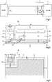
- the figure 1 shows an example of a supply line, connecting a source 1 to a load 3, protected by a protection device 5 such as that described in the aforementioned patent application.
- the source imposes a voltage V S across the terminals of the line.
- the device 5 is placed as close as possible to the load in order to protect it as well as possible from overvoltages which may occur on the line, for example following lightning strikes.
- the protection diode has a breakdown voltage greater than the voltage V S. In the absence of overvoltage, the diode is non-conducting. The switch SW is then open. When an overvoltage appears, the protection diode turns on. Once the overvoltage has passed, source 1 imposes in diode D a current greater than the holding current I h . The switch SW is then turned on which diverts the current flowing in the diode D in the switch SW. As a result, the current in the diode D normally becomes less than the holding current I h and, when the switch SW is reopened, the diode is reset.
- the aforementioned patent application proposes to control the switch SW on closing when the voltage V AK across the terminals of the diode becomes less than a first threshold voltage and to control the switch SW on opening when the voltage V AK becomes less than a second threshold voltage.
- the first threshold voltage corresponds to a value greater than the voltage imposed by the source 1 at the terminals of the diode when this diode is on.
- the second threshold voltage is lower than the voltage existing at the terminals of the diode when it is traversed by a current equal to the holding current Ih.
- the figure 2 is a sectional view showing an embodiment of a component 10 for protection against overvoltages and its electrical diagram.
- a metallization bonded to an anode electrode A is in contact with region 15 and a metallization bonded to a cathode electrode K is in contact with region 19.
- An emitter metallization bonded to the K electrode is in contact with the N-type region 24.
- a collector metallization bonded to a READ electrode is in contact with the substrate portion 13b through the region 23.
- a collector metallization bonded to a READ electrode is in contact with the substrate portion 13b through the region 23.
- a insulating layer 25 makes it possible to prevent the metallization K from coming into contact with parts of the substrate 13a-13b and with the layer 17 at the level of the transistor.
- An insulating layer 27 makes it possible to prevent the metallizations READ and A from coming into contact with parts of the substrate 13a-13b.
- Shockley diode D1 corresponds to a bipolar transistor T1 of PNP type connected to a bipolar transistor T2 of NPN type.
- the base of transistor T1 is connected to the collector of transistor T2, and the collector of transistor T1 is connected to the base of transistor T2.
- the emitter of transistor T1 corresponds to region 15 (anode), its base corresponds to portion 13a and its collector corresponds to region 17.
- the collector of transistor T2 corresponds to portion 13a, its base corresponds to region 17 and its emitter corresponds to region 19 (cathode).
- a transistor T2 ′ corresponds to transistor 21.
- the base of transistor T2 ′ is connected to the base of transistor T2.
- the collector of transistor T2 ′ corresponds to the portion of substrate 13b, its base corresponds to region 17 and its emitter corresponds to region 24.
- the transistors T2 and T2 ′ form a current mirror.
- the figure 3 is a top view of component 10 shown in sectional view in figure 2 .
- Transistor 21 is located in the top left corner of Shockley diode D1.
- the area of transistor T2 ′ is smaller than the area of diode D1.
- the ratio between the collector area of transistor T2 'and the collector area of transistor T2 is denoted k, k being a number greater than 1.
- transistors T2 and T2' are mounted as a current mirror, the current of collector of transistor T2 'will be k times lower than the collector current of transistor T2.
- the figure 4 is an electrical diagram of a protection device 30 comprising component 10, a detection and control circuit 33 and a switch SW.
- the electrodes A and K of component 10 are connected to a supply line, as in figure 1 .
- the detection and control circuit 33 comprises a resistor R1 connecting a voltage source VCC to the READ electrode of component 10, and a CONTROL control circuit connected on the one hand to the READ electrode and on the other hand to the READ electrode. SW switch control.
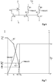
- the figure 5 is a timing diagram representing the collector current Ic2 'of transistor T2', the collector current Ic2 of transistor T2, and the voltage VREAD between the READ and K electrodes during an overvoltage.
- the operation of the protection device 30 is as follows.
- the Shockley diode D1 In the absence of an overvoltage, the Shockley diode D1 is non-conducting and the transistors T1, T2 and T2 ′ are non-conducting.
- the voltage VREAD is equal to VCC.
- the instant t1 corresponds to the moment when the current Ic2 becomes greater than a value k * Ic2'max. From this moment, the current Ic2 'is equal to the value Ic2'max and the voltage VREAD is equal to zero.
- the instant t3 corresponds to the moment when the CONTROL circuit detects that the voltage VREAD becomes greater than a first voltage threshold Vref1, which means that the current in the Shockley diode D1 has become less than a chosen value.
- the threshold Vref1 is for example chosen equal to VCC / 2.
- the CONTROL circuit then closes the switch SW after having verified that the voltage VREAD has passed through a substantially zero value. Due to the closing of the switch SW, the current flowing through the Shockley diode D1 and therefore the current Ic2 ′ decreases sharply. As a result, the voltage VREAD increases sharply.
- the instant t4 corresponds to the moment when the CONTROL circuit detects that the voltage VREAD becomes greater than a second voltage threshold Vref2.
- This second threshold is chosen to reflect the fact that the current in the Shockley diode D1 has become less than the holding current Ih of the Shockley diode D1.
- the CONTROL circuit then opens the switch SW and the Shockley diode D1 is reset.
- the switch SW is opened and closed as a function of the actual current flowing through the Shockley diode D1 and not as a function of the voltage at the terminals of the assembly of the Shockley diode D1 and of the switch SW.
- An advantage of controlling the switch SW to close as a function of the actual current flowing through the Shockley diode D1 is that the switch SW can be closed at a selected current value taking into account the possible presence mentioned above of a secondary peak of current at the end of the overvoltage.
- Another advantage of controlling the SW switch to open according to the actual current flowing through the Shockley diode D1 is that the current is not affected by the high frequency oscillations (linked to the switching of parasitic inductances) as can be the voltage V AK at the terminals of the Shockley diode and of the switch SW on closing of the switch SW.
- the CONTROL circuit opens the switch SW while the current in the Shockley diode is effectively less than the holding current Ih.
- the value of the current at which it is desired to close the switch SW is much greater (for example 50 times greater) than the value Ih.
- the voltage threshold Vref1 at which the switch SW is chosen to be closed is generally much smaller than the voltage threshold Vref2 at which the switch SW should be reopened.
- the voltage threshold Vref2 is very close to the voltage VCC, equal to VCC - ⁇ , with ⁇ very close to 0. It is therefore difficult to distinguish the threshold Vref2 from the voltage VCC and the CONTROL circuit risks opening the switch SW while the current in the Shockley diode D1 is still greater than the holding current Ih. The Shockley diode D1 then remains on. To avoid this drawback, the variant described in relation to the figures 6 and 7 .
- the figure 6 is an electrical diagram of an alternative embodiment of component 10 described in relation to the figures 2 and 3 .
- two read transistors T2 'and T2 are integrated. It is thus possible to obtain high detection sensitivities for very different current values, for example a current of the order of more than 50 A for the closing of the SW switch and a current of less than 1 A for its opening.
- the collectors of transistors T2 'and T2 "have the same areas, k times smaller than the area of the diode, and are connected to the voltage source VCC through resistors R1 and R2 distinct.
- the value of resistor R1 is less than the value of resistor R2.
- the figure 7 is a timing diagram representing the collector current Ic2 'of the transistor T2', the collector current Ic2 "of the transistor T2", the voltage VREAD1 of the collector of the transistor T2 ', and the voltage VREAD2 of the collector of the transistor T2 ".
- the switch SW is controlled on closing as a function of voltage VREAD1 and is controlled on opening as a function of voltage VREAD2.
- the switch SW is closed as before at an instant t3 when the collector current Ic2 ′ of the transistor T2 ′ becomes less than a chosen value (for example 1 / k times 50 A).
- the switch SW is open when the collector current Ic2 "of the transistor T2" becomes less than 1 / k times Ih (for example 1 / k times 1A).
- the current Ic2 is clipped to a value VCC / R2 markedly lower than the value VCC / R1 at which the current Ic2 'was clipped.
- the voltage VREAD2 is equal to the voltage threshold Vref2 equal to VCC / 2 when the current Ic2 "is equal to 1 / k times Ih.
- the voltage VREAD2 becomes less than the voltage threshold Vref2 because the current Ic2 "becomes less than 1 / k times Ih.
- the switch SW is then controlled to open and the diode is reblocked.
- the threshold Vref2 can, like the threshold Vref1, be far from the voltage VCC.
- the switch SW is therefore controlled on closing as well as opening without risk of error.
- the thresholds Vref1 and Vref2 can be equal, which makes it possible to generate only a single reference voltage.
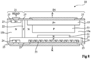
- the figure 8 is a sectional view of an example of a practical embodiment of the component 10 illustrated in a simplified in figures 2 and 3 .
- the Shockley diode D1 comprises, as previously, an N-type substrate 13a, an upper P-type layer 15, and a lower P-type region 17 in which an N-type region 19 is formed. It further comprises a region 51 of type N in contact with the upper face of region 17, and a region 53 of type P in contact with the underside of region 15. Regions 51 and 53 do not meet.
- region 19 is provided with emitter shorting holes 55.
- region 53 is produced by deep diffusion just like wall 22. We therefore take advantage of the step of manufacturing region 53 to manufacture wall 22.
- the wall 22 has been described as being a P-type semiconductor region.
- the wall 22 could also correspond to an insulating trench extending from the upper surface of the structure to the P-type region 17.
- resistors R1 and possibly R2 external to the integrated component has been described. Those skilled in the art will be able to provide for an integration of this or these resistors.
- the switch SW can for example be a MOS transistor or an insulated gate bipolar transistor (IGBT).
- IGBT insulated gate bipolar transistor
Landscapes
- Bipolar Integrated Circuits (AREA)
- Semiconductor Integrated Circuits (AREA)
- Electronic Switches (AREA)
- Electrodes Of Semiconductors (AREA)
Claims (7)
- Ein Bauelement (10), das Folgendes aufweist:
eine vertikale Shockley-Diode (D1), die von oben nach unten Folgendes umfasst:- einen ersten Bereich (15) eines ersten Leitfähigkeitstyps,- ein Substrat (13a) eines zweiten Leitfähigkeitstyps,- einen zweiten Bereich (17) des ersten Leitfähigkeitstyps, in dem ein dritter Bereich (19) des zweiten Leitfähigkeitstyps ausgebildet ist,wobei das Bauelement Folgendes aufweist:- eine erste Metallisierung, die mit dem ersten Bereich in Kontakt steht und mit einer Anodenelektrode (A) verbunden ist,- eine zweite Metallisierung, die mit dem dritten Bereich in Kontakt steht und mit einer Kathodenelektrode (K) verbunden ist,wobei das Bauelement ferner einen ersten vertikalen Transistor (T2') aufweist, wobei der Transistor von oben nach unten Folgendes umfasst:- einen Teil (13b) des Substrats, der von der Shockley-Diode (D1) durch eine vertikale Wand (22) getrennt ist,- einen Teil des zweiten Bereichs (17),- einen vierten Bereich (24) desselben Typs und mit derselben Dotierung wie der dritte Bereich (19), der in dem Teil des zweiten Bereichs (17) gebildet ist, wobei der dritte Bereich (19) mit dem vierten Bereich (24) verbunden ist, undwobei das Bauelement Folgendes aufweist:- eine dritte Metallisierung, die mit der Kathodenelektrode verbunden ist und mit dem vierten Bereich in Kontakt steht, wobei die Metallisierungen weder mit dem Substrat noch mit dem zweiten Bereich in Kontakt stehen;- eine vierte Metallisierung, die mit einer dritten Elektrode (READ) verbunden ist und die über einen hochdotierten Bereich des zweiten Leitfähigkeitstyps in Kontakt mit dem Teil (13b) des Substrats (13a) steht. - Bauelement nach Anspruch 1, das ferner einen zweiten Transistor (T2") mit derselben Struktur wie der erste Transistor (T2') aufweist.
- Bauelement nach Anspruch 1, wobei der erste Transistor (T2') in einer Ecke des Chips angeordnet ist, der die Shockley-Diode (D1) enthält.
- Schutzsystem (30), das Folgendes aufweist:ein Bauelement nach Anspruch 1;einen Schalter (SW), der parallel zu der Shockley-Diode (D1) geschaltet ist;einen Widerstand (R1), der einen ersten Anschluss hat, der mit dem Hauptanschluss des ersten Transistors verbunden ist, der der dritten Elektrode entspricht; undeine Spannungsquelle (VCC), die mit dem zweiten Anschluss des Widerstands (R1) verbunden ist,wobei der obere Hauptanschluss des ersten Transistors mit einer Schaltung zur Erfassung und Steuerung des Schalters (SW) verbunden ist.
- System nach Anspruch 4, wobei der Schalter (SW) so gesteuert wird, dass er in Abhängigkeit von der Spannung (VREAD) zwischen dem oberen Hauptanschluss des ersten Transistors und dem dritten Bereich (19) ein- und ausgeschaltet wird.
- Das Schutzsystem nach Anspruch 4, das weiterhin Folgendes aufweist:einen zweiten Transistor (T2") mit der gleichen Struktur wie der erste Transistor (T2'); undeinen zweiten Widerstand (R2), dessen erster Anschluss mit dem oberen Hauptanschluss des zweiten Transistors verbunden ist, und dessen zweiter Anschluss mit der Spannungsquelle (VCC) verbunden ist,wobei der obere Hauptanschluss des zweiten Transistors mit einer Schaltung zur Erfassung und Steuerung des Schalters (SW) verbunden ist.
- System nach Anspruch 6, wobei der Schalter (SW) gesteuert wird, um in Abhängigkeit von der ersten Spannung (VREAD1) zwischen dem oberen Hauptanschluss des ersten Transistors und dem dritten Bereich (19) eingeschaltet zu werden, und wobei der Schalter (SW) gesteuert wird, um in Abhängigkeit von der zweiten Spannung (VREAD2) zwischen dem oberen Hauptanschluss des zweiten Transistors und dem dritten Bereich (19) ausgeschaltet zu werden.
Applications Claiming Priority (1)
| Application Number | Priority Date | Filing Date | Title |
|---|---|---|---|
| FR1455999A FR3023060A1 (fr) | 2014-06-26 | 2014-06-26 | Composant de protection contre des surtensions |
Publications (2)
| Publication Number | Publication Date |
|---|---|
| EP2960938A1 EP2960938A1 (de) | 2015-12-30 |
| EP2960938B1 true EP2960938B1 (de) | 2021-03-31 |
Family
ID=52016665
Family Applications (1)
| Application Number | Title | Priority Date | Filing Date |
|---|---|---|---|
| EP15172650.2A Active EP2960938B1 (de) | 2014-06-26 | 2015-06-18 | Schutzkomponente gegen überspannungen |
Country Status (4)
| Country | Link |
|---|---|
| US (1) | US9685778B2 (de) |
| EP (1) | EP2960938B1 (de) |
| CN (3) | CN105226053B (de) |
| FR (1) | FR3023060A1 (de) |
Families Citing this family (4)
| Publication number | Priority date | Publication date | Assignee | Title |
|---|---|---|---|---|
| FR3023060A1 (fr) * | 2014-06-26 | 2016-01-01 | St Microelectronics Tours Sas | Composant de protection contre des surtensions |
| US9953973B1 (en) | 2017-03-15 | 2018-04-24 | International Business Machines Corporation | Diode connected vertical transistor |
| CN109509749A (zh) * | 2018-10-31 | 2019-03-22 | 上海长园维安微电子有限公司 | 一种利用可控硅双门极与阳极短路结构的单向负阻tvs器件及其制备方法 |
| CN114267717B (zh) * | 2021-11-19 | 2024-03-01 | 深圳深爱半导体股份有限公司 | 半导体器件及其制备方法 |
Family Cites Families (21)
| Publication number | Priority date | Publication date | Assignee | Title |
|---|---|---|---|---|
| FR1352864A (fr) | 1962-11-23 | 1964-02-21 | Perfectionnements aux tableaux de planning à rubans ou fils continus | |
| US5343053A (en) * | 1993-05-21 | 1994-08-30 | David Sarnoff Research Center Inc. | SCR electrostatic discharge protection for integrated circuits |
| FR2718899B1 (fr) * | 1994-04-14 | 1996-07-12 | Sgs Thomson Microelectronics | Indicateur de défaut d'un composant de protection. |
| US6411155B2 (en) * | 1994-12-30 | 2002-06-25 | Sgs-Thomson Microelectronics S.A. | Power integrated circuit |
| FR2734113B1 (fr) * | 1995-05-12 | 1997-07-25 | Sgs Thomson Microelectronics | Composant de protection complet de circuit d'interface de lignes d'abonnes |
| FR2750536B1 (fr) * | 1996-06-28 | 1998-12-18 | Sgs Thomson Microelectronics | Reseau de triacs a gachettes referencees par rapport a une electrode commune de face opposee |
| FR2753006B1 (fr) | 1996-08-27 | 1998-11-27 | Sgs Thomson Microelectronics | Pont redresseur protege monolithique |
| FR2800513B1 (fr) * | 1999-11-03 | 2002-03-29 | St Microelectronics Sa | Detecteur d'etat de composant de puissance |
| TW529153B (en) * | 2002-02-27 | 2003-04-21 | United Microelectronics Corp | Electrostatic discharge protection circuit |
| JP3899984B2 (ja) * | 2002-04-09 | 2007-03-28 | 富士電機デバイステクノロジー株式会社 | 過電圧保護回路 |
| GB0215089D0 (en) * | 2002-06-29 | 2002-08-07 | Power Innovations Ltd | Overvoltage protection |
| JP2006269902A (ja) * | 2005-03-25 | 2006-10-05 | Oki Electric Ind Co Ltd | 半導体集積回路 |
| TWI371989B (en) * | 2008-09-24 | 2012-09-01 | Richtek Technology Corp | Boost driver circuit with fast discharging function |
| US8390092B2 (en) * | 2010-11-12 | 2013-03-05 | Freescale Semiconductor, Inc. | Area-efficient high voltage bipolar-based ESD protection targeting narrow design windows |
| FR2969825B1 (fr) * | 2010-12-23 | 2013-07-12 | St Microelectronics Tours Sas | Composant vertical bidirectionnel a double sillonnage |
| FR2974447A1 (fr) * | 2011-04-22 | 2012-10-26 | St Microelectronics Tours Sas | Structure d'amorcage et composant de protection comprenant une telle structure d'amorcage |
| CN202840947U (zh) * | 2012-07-05 | 2013-03-27 | 意法半导体研发(上海)有限公司 | 稳压电荷泵电路 |
| US8692289B2 (en) * | 2012-07-25 | 2014-04-08 | Taiwan Semiconductor Manufacturing Company, Ltd. | Fast turn on silicon controlled rectifiers for ESD protection |
| CN103811482B (zh) * | 2012-11-14 | 2016-08-03 | 旺宏电子股份有限公司 | 静电放电保护电路 |
| FR3004019A1 (fr) | 2013-03-29 | 2014-10-03 | St Microelectronics Tours Sas | Composant de protection contre des surtensions |
| FR3023060A1 (fr) * | 2014-06-26 | 2016-01-01 | St Microelectronics Tours Sas | Composant de protection contre des surtensions |
-
2014
- 2014-06-26 FR FR1455999A patent/FR3023060A1/fr active Pending
-
2015
- 2015-05-29 US US14/725,342 patent/US9685778B2/en active Active
- 2015-06-18 EP EP15172650.2A patent/EP2960938B1/de active Active
- 2015-06-26 CN CN201510363846.6A patent/CN105226053B/zh active Active
- 2015-06-26 CN CN201910023468.5A patent/CN109473428B/zh active Active
- 2015-06-26 CN CN201520449978.6U patent/CN204966493U/zh not_active Withdrawn - After Issue
Non-Patent Citations (1)
| Title |
|---|
| None * |
Also Published As
| Publication number | Publication date |
|---|---|
| CN105226053A (zh) | 2016-01-06 |
| CN109473428B (zh) | 2023-11-03 |
| CN204966493U (zh) | 2016-01-13 |
| EP2960938A1 (de) | 2015-12-30 |
| US9685778B2 (en) | 2017-06-20 |
| US20150380925A1 (en) | 2015-12-31 |
| FR3023060A1 (fr) | 2016-01-01 |
| CN105226053B (zh) | 2019-02-05 |
| CN109473428A (zh) | 2019-03-15 |
Similar Documents
| Publication | Publication Date | Title |
|---|---|---|
| EP0714139B1 (de) | Zweipoliges Bauteil zur Überkopfzündung mit kontrollierter Empfindlichkeit | |
| EP2960938B1 (de) | Schutzkomponente gegen überspannungen | |
| FR2916574A1 (fr) | Dispositif a semi-conducteur | |
| EP0687051B1 (de) | Telefonleitungs-Interface-Schutz | |
| EP0742591B1 (de) | Bauelement für den vollständigen Schutz einer Schnittstellenschaltung von Teilnehmerleitungen | |
| EP0963608A1 (de) | Schaltungsanordnung zum schutz von teilnehmerschnittstellen | |
| EP3070798B1 (de) | Schutzvorrichtung gegen überspannungen | |
| FR3039014B1 (fr) | Protection de ligne telephonique contre les surtensions | |
| EP3276662B1 (de) | Struktur zum schutz eines integrierten schaltkreises gegen elektrostatische entladungen | |
| EP1076365B1 (de) | Empfindlicher statischer Zweirichtungsschalter | |
| EP0881687B1 (de) | Kontakt auf P-Typ Gebiet | |
| EP0599739B1 (de) | Thyristor und Aufbau von Thyristoren mit gemeinsamer Katode | |
| EP3863140A1 (de) | Schutz gegen überspannungen | |
| EP1544919B1 (de) | Triac | |
| EP1076366A1 (de) | Zweirichtungsschalter mit verbesserten Schaltleistungen | |
| EP2348528A1 (de) | Schutzvorrichtung für einen integrierten Schaltkreis gegen elektrostatische Entladungen | |
| EP0865671B1 (de) | Normal leitender dual-thyristor | |
| EP0742592A1 (de) | Empfindliches Schutzbauelement für Schnittstellenschaltung von Teilnehmerleitungen | |
| FR2818805A1 (fr) | Commutateur statique bidirectionnel sensible | |
| FR3097682A1 (fr) | Composant monolithique comportant un transistor de puissance au nitrure de gallium | |
| FR2988883A1 (fr) | Modele de simulation de thyristor | |
| EP3091572B1 (de) | Bidirektioneller leistungsschalter | |
| EP0055644A1 (de) | MOS-Transistor mit bipolarer Wirkungsweise wenn in Sättigung betrieben | |
| FR2764735A1 (fr) | Protection du caisson logique d'un composant incluant un transistor mos de puissance integre | |
| FR2616271A1 (fr) | Circuit integre comprenant en particulier un mesfet protege contre les courants de fuites, sur substrat semi-isolant |
Legal Events
| Date | Code | Title | Description |
|---|---|---|---|
| PUAI | Public reference made under article 153(3) epc to a published international application that has entered the european phase |
Free format text: ORIGINAL CODE: 0009012 |
|
| 17P | Request for examination filed |
Effective date: 20150618 |
|
| AK | Designated contracting states |
Kind code of ref document: A1 Designated state(s): AL AT BE BG CH CY CZ DE DK EE ES FI FR GB GR HR HU IE IS IT LI LT LU LV MC MK MT NL NO PL PT RO RS SE SI SK SM TR |
|
| AX | Request for extension of the european patent |
Extension state: BA ME |
|
| STAA | Information on the status of an ep patent application or granted ep patent |
Free format text: STATUS: EXAMINATION IS IN PROGRESS |
|
| 17Q | First examination report despatched |
Effective date: 20190430 |
|
| GRAP | Despatch of communication of intention to grant a patent |
Free format text: ORIGINAL CODE: EPIDOSNIGR1 |
|
| STAA | Information on the status of an ep patent application or granted ep patent |
Free format text: STATUS: GRANT OF PATENT IS INTENDED |
|
| INTG | Intention to grant announced |
Effective date: 20201120 |
|
| GRAS | Grant fee paid |
Free format text: ORIGINAL CODE: EPIDOSNIGR3 |
|
| GRAA | (expected) grant |
Free format text: ORIGINAL CODE: 0009210 |
|
| STAA | Information on the status of an ep patent application or granted ep patent |
Free format text: STATUS: THE PATENT HAS BEEN GRANTED |
|
| AK | Designated contracting states |
Kind code of ref document: B1 Designated state(s): AL AT BE BG CH CY CZ DE DK EE ES FI FR GB GR HR HU IE IS IT LI LT LU LV MC MK MT NL NO PL PT RO RS SE SI SK SM TR |
|
| REG | Reference to a national code |
Ref country code: GB Ref legal event code: FG4D Free format text: NOT ENGLISH Ref country code: CH Ref legal event code: EP |
|
| REG | Reference to a national code |
Ref country code: AT Ref legal event code: REF Ref document number: 1377908 Country of ref document: AT Kind code of ref document: T Effective date: 20210415 |
|
| REG | Reference to a national code |
Ref country code: DE Ref legal event code: R096 Ref document number: 602015067390 Country of ref document: DE |
|
| REG | Reference to a national code |
Ref country code: IE Ref legal event code: FG4D Free format text: LANGUAGE OF EP DOCUMENT: FRENCH |
|
| REG | Reference to a national code |
Ref country code: LT Ref legal event code: MG9D |
|
| PG25 | Lapsed in a contracting state [announced via postgrant information from national office to epo] |
Ref country code: BG Free format text: LAPSE BECAUSE OF FAILURE TO SUBMIT A TRANSLATION OF THE DESCRIPTION OR TO PAY THE FEE WITHIN THE PRESCRIBED TIME-LIMIT Effective date: 20210630 Ref country code: NO Free format text: LAPSE BECAUSE OF FAILURE TO SUBMIT A TRANSLATION OF THE DESCRIPTION OR TO PAY THE FEE WITHIN THE PRESCRIBED TIME-LIMIT Effective date: 20210630 Ref country code: FI Free format text: LAPSE BECAUSE OF FAILURE TO SUBMIT A TRANSLATION OF THE DESCRIPTION OR TO PAY THE FEE WITHIN THE PRESCRIBED TIME-LIMIT Effective date: 20210331 Ref country code: HR Free format text: LAPSE BECAUSE OF FAILURE TO SUBMIT A TRANSLATION OF THE DESCRIPTION OR TO PAY THE FEE WITHIN THE PRESCRIBED TIME-LIMIT Effective date: 20210331 |
|
| PG25 | Lapsed in a contracting state [announced via postgrant information from national office to epo] |
Ref country code: LV Free format text: LAPSE BECAUSE OF FAILURE TO SUBMIT A TRANSLATION OF THE DESCRIPTION OR TO PAY THE FEE WITHIN THE PRESCRIBED TIME-LIMIT Effective date: 20210331 Ref country code: RS Free format text: LAPSE BECAUSE OF FAILURE TO SUBMIT A TRANSLATION OF THE DESCRIPTION OR TO PAY THE FEE WITHIN THE PRESCRIBED TIME-LIMIT Effective date: 20210331 Ref country code: SE Free format text: LAPSE BECAUSE OF FAILURE TO SUBMIT A TRANSLATION OF THE DESCRIPTION OR TO PAY THE FEE WITHIN THE PRESCRIBED TIME-LIMIT Effective date: 20210331 |
|
| REG | Reference to a national code |
Ref country code: NL Ref legal event code: MP Effective date: 20210331 |
|
| REG | Reference to a national code |
Ref country code: AT Ref legal event code: MK05 Ref document number: 1377908 Country of ref document: AT Kind code of ref document: T Effective date: 20210331 |
|
| PG25 | Lapsed in a contracting state [announced via postgrant information from national office to epo] |
Ref country code: SM Free format text: LAPSE BECAUSE OF FAILURE TO SUBMIT A TRANSLATION OF THE DESCRIPTION OR TO PAY THE FEE WITHIN THE PRESCRIBED TIME-LIMIT Effective date: 20210331 Ref country code: CZ Free format text: LAPSE BECAUSE OF FAILURE TO SUBMIT A TRANSLATION OF THE DESCRIPTION OR TO PAY THE FEE WITHIN THE PRESCRIBED TIME-LIMIT Effective date: 20210331 Ref country code: EE Free format text: LAPSE BECAUSE OF FAILURE TO SUBMIT A TRANSLATION OF THE DESCRIPTION OR TO PAY THE FEE WITHIN THE PRESCRIBED TIME-LIMIT Effective date: 20210331 Ref country code: LT Free format text: LAPSE BECAUSE OF FAILURE TO SUBMIT A TRANSLATION OF THE DESCRIPTION OR TO PAY THE FEE WITHIN THE PRESCRIBED TIME-LIMIT Effective date: 20210331 Ref country code: NL Free format text: LAPSE BECAUSE OF FAILURE TO SUBMIT A TRANSLATION OF THE DESCRIPTION OR TO PAY THE FEE WITHIN THE PRESCRIBED TIME-LIMIT Effective date: 20210331 Ref country code: AT Free format text: LAPSE BECAUSE OF FAILURE TO SUBMIT A TRANSLATION OF THE DESCRIPTION OR TO PAY THE FEE WITHIN THE PRESCRIBED TIME-LIMIT Effective date: 20210331 |
|
| PG25 | Lapsed in a contracting state [announced via postgrant information from national office to epo] |
Ref country code: IS Free format text: LAPSE BECAUSE OF FAILURE TO SUBMIT A TRANSLATION OF THE DESCRIPTION OR TO PAY THE FEE WITHIN THE PRESCRIBED TIME-LIMIT Effective date: 20210731 Ref country code: ES Free format text: LAPSE BECAUSE OF FAILURE TO SUBMIT A TRANSLATION OF THE DESCRIPTION OR TO PAY THE FEE WITHIN THE PRESCRIBED TIME-LIMIT Effective date: 20210331 Ref country code: PT Free format text: LAPSE BECAUSE OF FAILURE TO SUBMIT A TRANSLATION OF THE DESCRIPTION OR TO PAY THE FEE WITHIN THE PRESCRIBED TIME-LIMIT Effective date: 20210802 Ref country code: PL Free format text: LAPSE BECAUSE OF FAILURE TO SUBMIT A TRANSLATION OF THE DESCRIPTION OR TO PAY THE FEE WITHIN THE PRESCRIBED TIME-LIMIT Effective date: 20210331 Ref country code: SK Free format text: LAPSE BECAUSE OF FAILURE TO SUBMIT A TRANSLATION OF THE DESCRIPTION OR TO PAY THE FEE WITHIN THE PRESCRIBED TIME-LIMIT Effective date: 20210331 Ref country code: RO Free format text: LAPSE BECAUSE OF FAILURE TO SUBMIT A TRANSLATION OF THE DESCRIPTION OR TO PAY THE FEE WITHIN THE PRESCRIBED TIME-LIMIT Effective date: 20210331 |
|
| REG | Reference to a national code |
Ref country code: DE Ref legal event code: R097 Ref document number: 602015067390 Country of ref document: DE |
|
| PG25 | Lapsed in a contracting state [announced via postgrant information from national office to epo] |
Ref country code: DK Free format text: LAPSE BECAUSE OF FAILURE TO SUBMIT A TRANSLATION OF THE DESCRIPTION OR TO PAY THE FEE WITHIN THE PRESCRIBED TIME-LIMIT Effective date: 20210331 Ref country code: AL Free format text: LAPSE BECAUSE OF FAILURE TO SUBMIT A TRANSLATION OF THE DESCRIPTION OR TO PAY THE FEE WITHIN THE PRESCRIBED TIME-LIMIT Effective date: 20210331 Ref country code: MC Free format text: LAPSE BECAUSE OF FAILURE TO SUBMIT A TRANSLATION OF THE DESCRIPTION OR TO PAY THE FEE WITHIN THE PRESCRIBED TIME-LIMIT Effective date: 20210331 |
|
| REG | Reference to a national code |
Ref country code: CH Ref legal event code: PL |
|
| PLBE | No opposition filed within time limit |
Free format text: ORIGINAL CODE: 0009261 |
|
| STAA | Information on the status of an ep patent application or granted ep patent |
Free format text: STATUS: NO OPPOSITION FILED WITHIN TIME LIMIT |
|
| GBPC | Gb: european patent ceased through non-payment of renewal fee |
Effective date: 20210630 |
|
| 26N | No opposition filed |
Effective date: 20220104 |
|
| REG | Reference to a national code |
Ref country code: BE Ref legal event code: MM Effective date: 20210630 |
|
| PG25 | Lapsed in a contracting state [announced via postgrant information from national office to epo] |
Ref country code: LU Free format text: LAPSE BECAUSE OF NON-PAYMENT OF DUE FEES Effective date: 20210618 |
|
| PG25 | Lapsed in a contracting state [announced via postgrant information from national office to epo] |
Ref country code: LI Free format text: LAPSE BECAUSE OF NON-PAYMENT OF DUE FEES Effective date: 20210630 Ref country code: IE Free format text: LAPSE BECAUSE OF NON-PAYMENT OF DUE FEES Effective date: 20210618 Ref country code: GB Free format text: LAPSE BECAUSE OF NON-PAYMENT OF DUE FEES Effective date: 20210630 Ref country code: CH Free format text: LAPSE BECAUSE OF NON-PAYMENT OF DUE FEES Effective date: 20210630 |
|
| PG25 | Lapsed in a contracting state [announced via postgrant information from national office to epo] |
Ref country code: IS Free format text: LAPSE BECAUSE OF FAILURE TO SUBMIT A TRANSLATION OF THE DESCRIPTION OR TO PAY THE FEE WITHIN THE PRESCRIBED TIME-LIMIT Effective date: 20210731 Ref country code: FR Free format text: LAPSE BECAUSE OF NON-PAYMENT OF DUE FEES Effective date: 20210630 |
|
| PG25 | Lapsed in a contracting state [announced via postgrant information from national office to epo] |
Ref country code: IT Free format text: LAPSE BECAUSE OF FAILURE TO SUBMIT A TRANSLATION OF THE DESCRIPTION OR TO PAY THE FEE WITHIN THE PRESCRIBED TIME-LIMIT Effective date: 20210331 Ref country code: BE Free format text: LAPSE BECAUSE OF NON-PAYMENT OF DUE FEES Effective date: 20210630 |
|
| PG25 | Lapsed in a contracting state [announced via postgrant information from national office to epo] |
Ref country code: HU Free format text: LAPSE BECAUSE OF FAILURE TO SUBMIT A TRANSLATION OF THE DESCRIPTION OR TO PAY THE FEE WITHIN THE PRESCRIBED TIME-LIMIT; INVALID AB INITIO Effective date: 20150618 |
|
| PG25 | Lapsed in a contracting state [announced via postgrant information from national office to epo] |
Ref country code: CY Free format text: LAPSE BECAUSE OF FAILURE TO SUBMIT A TRANSLATION OF THE DESCRIPTION OR TO PAY THE FEE WITHIN THE PRESCRIBED TIME-LIMIT Effective date: 20210331 |
|
| PG25 | Lapsed in a contracting state [announced via postgrant information from national office to epo] |
Ref country code: GR Free format text: LAPSE BECAUSE OF FAILURE TO SUBMIT A TRANSLATION OF THE DESCRIPTION OR TO PAY THE FEE WITHIN THE PRESCRIBED TIME-LIMIT Effective date: 20210331 |
|
| PG25 | Lapsed in a contracting state [announced via postgrant information from national office to epo] |
Ref country code: MK Free format text: LAPSE BECAUSE OF FAILURE TO SUBMIT A TRANSLATION OF THE DESCRIPTION OR TO PAY THE FEE WITHIN THE PRESCRIBED TIME-LIMIT Effective date: 20210331 |
|
| PG25 | Lapsed in a contracting state [announced via postgrant information from national office to epo] |
Ref country code: MT Free format text: LAPSE BECAUSE OF FAILURE TO SUBMIT A TRANSLATION OF THE DESCRIPTION OR TO PAY THE FEE WITHIN THE PRESCRIBED TIME-LIMIT Effective date: 20210331 |
|
| REG | Reference to a national code |
Ref country code: DE Ref legal event code: R079 Ref document number: 602015067390 Country of ref document: DE Free format text: PREVIOUS MAIN CLASS: H01L0027070000 Ipc: H10D0084000000 |
|
| PGFP | Annual fee paid to national office [announced via postgrant information from national office to epo] |
Ref country code: DE Payment date: 20250520 Year of fee payment: 11 |
|
| PG25 | Lapsed in a contracting state [announced via postgrant information from national office to epo] |
Ref country code: TR Free format text: LAPSE BECAUSE OF FAILURE TO SUBMIT A TRANSLATION OF THE DESCRIPTION OR TO PAY THE FEE WITHIN THE PRESCRIBED TIME-LIMIT Effective date: 20210331 |