EP0601207A1 - Methode de lecture de donnees et circuit de memoire morte - Google Patents
Methode de lecture de donnees et circuit de memoire morte Download PDFInfo
- Publication number
- EP0601207A1 EP0601207A1 EP93913597A EP93913597A EP0601207A1 EP 0601207 A1 EP0601207 A1 EP 0601207A1 EP 93913597 A EP93913597 A EP 93913597A EP 93913597 A EP93913597 A EP 93913597A EP 0601207 A1 EP0601207 A1 EP 0601207A1
- Authority
- EP
- European Patent Office
- Prior art keywords
- potential
- column
- bit line
- potential level
- line
- Prior art date
- Legal status (The legal status is an assumption and is not a legal conclusion. Google has not performed a legal analysis and makes no representation as to the accuracy of the status listed.)
- Granted
Links
- 238000000034 method Methods 0.000 title claims description 10
- 230000004044 response Effects 0.000 claims description 8
- 238000010586 diagram Methods 0.000 description 5
- 239000011159 matrix material Substances 0.000 description 4
- 230000006870 function Effects 0.000 description 3
- 238000007599 discharging Methods 0.000 description 2
- 230000005611 electricity Effects 0.000 description 2
- 230000003247 decreasing effect Effects 0.000 description 1
- 230000010354 integration Effects 0.000 description 1
- 239000004065 semiconductor Substances 0.000 description 1
Images

Classifications
-
- G—PHYSICS
- G11—INFORMATION STORAGE
- G11C—STATIC STORES
- G11C17/00—Read-only memories programmable only once; Semi-permanent stores, e.g. manually-replaceable information cards
- G11C17/08—Read-only memories programmable only once; Semi-permanent stores, e.g. manually-replaceable information cards using semiconductor devices, e.g. bipolar elements
- G11C17/10—Read-only memories programmable only once; Semi-permanent stores, e.g. manually-replaceable information cards using semiconductor devices, e.g. bipolar elements in which contents are determined during manufacturing by a predetermined arrangement of coupling elements, e.g. mask-programmable ROM
- G11C17/12—Read-only memories programmable only once; Semi-permanent stores, e.g. manually-replaceable information cards using semiconductor devices, e.g. bipolar elements in which contents are determined during manufacturing by a predetermined arrangement of coupling elements, e.g. mask-programmable ROM using field-effect devices
- G11C17/126—Virtual ground arrays
-
- G—PHYSICS
- G11—INFORMATION STORAGE
- G11C—STATIC STORES
- G11C16/00—Erasable programmable read-only memories
- G11C16/02—Erasable programmable read-only memories electrically programmable
- G11C16/06—Auxiliary circuits, e.g. for writing into memory
- G11C16/26—Sensing or reading circuits; Data output circuits
Definitions
- the present invention relates to a read-only memory circuit (ROM circuit) such as an erasable programmable read-only memory (EPROM).
- ROM circuit read-only memory circuit
- EPROM erasable programmable read-only memory
- the NOR type is more effective than the NAND type in respect of high-speed reading but is larger than the latter in respect of the occupying area of the memory cell.
- Such a ROM circuit is disclosed in e.g. Japanese Patent Laid-Open Publication No. 1-259556 as published in October 17, 1989 and No. 4-74395 as published in March 9, 1992.
- a method of reading data comprising the steps of selecting a given column line and a bit line which adjoins to the column line among a plurality of column and bit lines in response to a column selection signal, selecting a given row line among a plurality of row lines in response to a row selection signal, and reading out data which is stored in a memory cell connected to the given column and row lines to the selected bit line; data is read out from the memory cell by setting the given column line to be at a first potential level and almost at the same time by setting the selected bit line to be at a second potential level which is lower than the first potential level and setting unselected column lines at a third potential which is lower than the second potential.
- a read-only memory circuit comprises a plurality of column lines, a plurality of bit lines arranged with the column lines in turns in parallel thereto, a plurality of row lines arranged substantially at right angles to the bit and column lines, a plurality of memory cells for storing data therein, each memory cell having a control terminal coupled to the row lines and being coupled between the column lines and the bit lines, a row selection circuit for selecting a given row line among the plural row lines, a column selection circuit for selecting a given column line among the plural column lines and the bit line adjoining to the selected column line to read out data stored in the memory cell which is coupled to the selected row and column lines, a first potential supply circuit for applying a first potential to the selected column line, a second potential supply circuit for applying a second potential which is lower than the first potential to the selected bit line and a third potential supply circuit for applying a third potential which is lower than the second potential to unselected column lines.
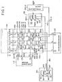
- Fig. 1 is a block diagram of a main portion of a ROM circuit according to a first embodiment of the present invention
- Fig. 2 is a block diagram of a ROM circuit according to a second embodiment of the present invention
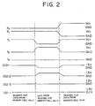
- Fig. 3 is a timing chart showing the operation of the ROM circuit illustrated in Figs. 1 and 2
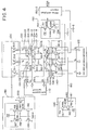
- Fig. 4 is a block diagram of a ROM circuit according to a third embodiment of the present invention.
- Fig. 1 is a block diagram of a read-only memory circuit (referred to as a ROM circuit hereinafter) according to a first embodiment of the present invention.
- the ROM circuit is equipped with a memory matrix 100, a row address decoder 110 serving as a row selection means, a column address decoder 120 serving as a column selection means, a pulldown circuit 130, a multiplexer 140, a sense amplifier circuit 150 and an inner voltage regulator circuit 160.
- the memory matrix 100 is a circuit for storing data therein.
- the memory matrix 100 comprises bit lines 101-1 and 101-2 and column lines 102-1, 102-2 and 102-3, the bit and column lines being arranged in turns, and row lines 103-1 to 103-n arranged substantially at right angles to the bit and column lines.
- Memory cells 104-01 to 104-04, 104-11 to 104-14, ..., 104-n1 to 104-n4 composed of n-channel MOS transistors (referred to as NMOS hereinafter) are provided between each adjacent pair of bit lines 101-1 and 101-2 and column lines 102-1, 102-2 and 102-3.
- Each of the memory cells 104-01 to 104-n4 is coupled to each corresponding column line of the column lines 102-1 to 102-3 at the source electrode thereof (referred to simply as a source hereinafter), to each of the bit lines 101-1 and 101-2 at the drain electrode thereof (referred to simply as a drain hereinafter) and to each corresponding row line of the row lines 103-1 to 103-n at the gate electrode thereof (referred to simply as a gate hereinafter).
- the row address decoder 110 is coupled to the row lines 103-1 to 103-n.
- the row address decoder 110 decodes a row address signal inputted thereto and supplies a plurality of row selection signal X0 to X n to the row lines 103-1 to 103-n respectively.
- the column address decoder 120 is a circuit which decodes the column address signal inputted thereto and produces a plurality of column selection signals Y1 to Y3 for selecting the bit lines 101-1 and 101-2 and the column lines 102-1 to 102-3.
- the multiplexer 140 is a circuit which is coupled to the bit lines 101-1 and 101-2 and the column lines 102-1 to 102-3 and selects one of the pairs of the bit lines 101-1 and 101-2 and the column lines 102-1 to 102-3 based on the column selection signals Y1 to Y3.
- the multiplexer 140 is composed of a plurality of switching NMOSs 141-1 to 141-4 and NMOSs 142-1 to 142-3. Each switching NMOSs 141-1 to 141-4 are respectively turned on or off by the column selection signals Y1, Y2 and Y3. Among them the NMOSs 141-1 and 141-2 are coupled between the bit lines 101-1 and a data bus 170-1.
- the NMOSs 141-3 and 141-4 are coupled between the bit line 101-2 and a data bus 170-2.
- the NMOSs 142-1 to 142-3 are respectively turned on or of by the column selection signals Y1, Y2 and Y3, and are coupled between the column lines 142-1 to 142-3 and GND (ground) respectively.
- the pull-down circuit 130 is composed of NMOSs 131-1 to 131-3 which are respectively coupled to the column lines 102-1 to 102-3. Each NMOS is coupled to GND (ground) at the source thereof.
- the NMOSs 131-1 to 131-3 receive the inversed signals Y ⁇ 1, Y ⁇ 2 and Y ⁇ 3 of the column selection signals Y1, Y2 and Y3 respectively at the gates thereof.
- the inner voltage regulator circuit 160 is coupled to the column lines 102-1 to 102-3 by way of the multiplexer 140.
- the inner voltage regulator circuit 160 comprises a CMOS inverter composed of a p-channel MOS transistor (referred to as PMOS hereinafter) 161 and an NMOS 162 coupled between V cc (power source) and GND (ground) in series, an NMOS 165 which is coupled between V cc and an inner output node N 163 and the gate of which is coupled to the output node N 164 of the inverter, an NMOS 166 which is coupled between the node N 164 and GND and the gate of which is coupled to the output node N 163 and a high resistant element 167 coupled between the output node N 163 and GND.
- An inner control signal CE ⁇ for controlling the standby-state/operating-state in reading out data is supplied to the input terminal of the CMOS inverter, i.e., to the gates of the PMOS 161 and the NMOS 162.
- the output voltage is designed to be on the order of 1.5 V according to this embodiment, but in case of a mask ROM etc., the power source V cc can be employed instead of a built-in constant voltage source.
- the inner voltage regulator circuit is not limited to that described in this embodiment, but can be anything which can produce a potential excepting the GND level.
- the sense amplifier circuit 150 is a circuit which amplifies a change in potential in the data bus 170 and outputs the same.
- the sense amplifier circuit 150-1 thereof is composed of a first resistor element 153 coupled between a sense input node N 154 and GND, an NMOS 152 which is coupled between a sense output node N 155 and a sense input node N 155 and the gate of which is coupled to a power source V cons which supplies a constant voltage thereto and a PMOS 151 which is coupled between V cc and the output node N 155 and the gate of which receives the control signal CE ⁇ .
- the sense amplifier circuit 150-2 is the same as the sense amplifier circuit 150-1 in circuit arrangement.
- the sense input node is coupled to the data bus 170-2 to amplify a change in potential in the data bus 170-2 and supplies the same to a sense output node N156.
- the resistor values of the first resistor element 153, the PMOS 151 when it is turned on and the NMOS 152 when it is turned on are set so that the sense input may be about 0.1 V.
- This setting has the following two merits.
- the first is that the sense input at the expected value "H' or "L", i.e., the amplitude of the potential in the bit lines can be made small since the input impedance of the sense amplifier circuit can be made small. That is, it is advantageous in highspeed access since the time for charging and discharging the bit lines having a capacitance of several PFs can be shortened in reading operation.
- the second is that it does not influence the current in the selected memory cell.
- the potential of the selected bit line is set to be as close to 0 V as possible in order to obtain a memory cell current substantially as much as in the conventional system.
- the reading operation of the data bus 170-1 system coupled to the sense amplifier circuit 150-1 by way of the memory cells 104-01, 104-02, 104-11 and 104-12 will be described with reference to the signal waveform diagram illustrated in Fig. 3.
- the data bus 170-2 system may be considered to operate in the same way.
- V ⁇ threshold value
- V cc level power source potential level
- the row selection signal X1 and the column selection signal Y1 are at V cc level and the row selection signals X0, X2 to X n and the column selection signals Y2 and Y3 are at GND level.
- the inverse signals Y ⁇ 2 and Y ⁇ 3 of the column selection signals Y2 and Y3 are at V cc level and Y ⁇ 1 of the column selection signal Y1 is at GND level.
- the NMOSs 141-2, 141-3, 141-4, 142-2 and 142-3 are turned off and the NMOSs 131-2 and 131-3 are turned on, so that the unselected column lines 102-2 and 102-3 and the bit line 101-2 is at GND level.
- the selected column line 102-1 is electrically connected with a bias bus 180 since the NMOS 142-1 is turned on, so that the potential level thereof becomes as high as the output voltage 1.5 V of the inner voltage regulator circuit 160.
- the selected bit line 101-1 is electrically connected with the data bus 170-1 since the NMOS 141-1 is turned on. As a result, the potential of the data bus 170-1 is as high as the input voltage 0.1 V of the sense amplifier circuit 150-1.
- the sense amplifier circuit 150-1 detects data which has been written in the memory cell 104-11 by the current generated by the memory cell 104-11. Since there is a voltage of 0.1 V between the source and drain of the memory cell 104-12 on the same row selecting line adjoining to the memory cell 104-11, there exists a leak current due to the data written in the memory cell 104-12. The leak current, however, does not cause any trouble since the voltage between the source and drain of the unselected memory cell is about 0.1 V and the leak current can be set lower than 1/10 of the selected memory cell even if the floating potential 0.1 V at the source of the selected memory cell is taken into consideration.
- the selected memory cell 104-01 supplies current to the sense amplifier circuit 150-1 by way of the NMOS 141-1.
- the sense amplifier circuit 150-1 converts the current supplied thereto into a voltage and amplifies the voltage to apply the same to the output node N 155.
- the selected column line 102-2 becomes in potential as high as the output potential 1.5 V of the inner voltage regulator circuit 160 since the NMOS 142-2 is turned on and the NMOS 131-2 is turned off.
- the unselected column line 102-1 is at the potential when it is not selected, i.e., GND level since the NMOS 131-1 is turned on and the NMOS 142-1 is turned off. Since the NMOS 141-1 is turned off and the NMOS 141-2 is turned on, the bit line 101-1 is electrically connected with the sense amplifier circuit 150-1 and the data stored in the selected memory cell 104-12 is read out to the bit line 101-1. In this case, since the data stored in the memory cell 104-11 and that stored in the memory cell 104-12 are the same with each other, the states of the selected bit line 101-1 and the sense amplifier circuit 150-1 remain unchanged.
- the row selection signal X0 and the column selection signal Y1 go V cc level and the row selection signals X1 to X n and the column selection signals Y2 and Y3 go GND level so that the operation steps forwards to reading data in the memory cell 104-01 will be described hereinafter. Since the NMOS 142-1 is turned on and the inverse signal Y ⁇ 1 of the column selection signal Y1 is at GND level so that the NMOS 131-1 is turned off, the selected column line 102-1 is electrically connected with the output of the inner voltage regulator circuit 160 to be 1.5 V in potential.
- the potential of the unselected column line 102-2 is at GND level. Since the threshold value V ⁇ of the selected memory cell 104-01 is higher than the V cc level, the bit line 101-1 which no longer receive current passing from the memory cells thereto shifts to the potential of "L" level at the time of reading data.
- control signal CE ⁇ is at "H' level, i.e., a standby state
- the row selection signals X0 to X n and the column selection signals Y1 to Y3 are at GND level. It is not always a necessary condition, but it is enough that either of the row or column selection signals are all at GND level so that there is no current between the source and drain of all the memory cells.
- the inverse signals Y ⁇ 1, Y ⁇ 2 and Y ⁇ 3 of the column selection signals go all V cc level.
- the PMOS 161 is turned off and the NMOS 162 is turned on so that the N 164 is at GND level and the NMOS 165 is turned off.
- the output of the inner voltage regulator circuit 160 goes GND level due to the high resistant element 167, so that there is no D/C consumption in the circuit.
- the control signal CE ⁇ is at V cc level also in the sense amplifier circuit 150-1, there is no current directly passing from the power source V cc to GND.
- the sense input N 154 goes GND level by way of the resistor element 153.
- the sense amplifier circuit 150-1 Since the state where the sense input is 0.1 V is a stationary state, the sense amplifier circuit 150-1 charges the data bus 170-1 and a selected bit line with electricity to be 0.1 V in potential. The sense amplifier circuit 150-1, the data bus 170-1 and the selected bit line are ready to read out the data from the selected memory cell instantly after they are in an operating state.
- the N 164 of the inner voltage regulator circuit 160 goes V cc level instantly after the control signal CE ⁇ goes "L" level, and starts charging the bias bus 180 with electricity to be 1.5 V in potential by way of the NMOS 165. It is possible to charge the bias bus 180 instantly up to 1.5 V in potential since the load of the inner voltage regulator circuit 160 is the selected column line alone when the inner voltage regulator circuit 160 is switched from a standby state to an operating state.
- FIG. 3 A second embodiment of the present invention will be described with reference to Fig. 3.
- same elements illustrated in Fig. 1 are denoted at same numerals. The functions thereof are easily understandable from the above description.
- the column lines 102-1, 102-2 and 102-3 are coupled to the inner voltage regulator circuits 160-1, 160-2 and 160-3 by way of bias buses 180-1, 180-2 and 180-3 respectively.
- the column address selection signals Y1, Y2 and Y3 are supplied to the inner voltage regulator circuits 160-1, 160-2 and 160-3 respectively.
- These inner voltage regulator circuits are the same with one another in arrangement, so the inner voltage regulator circuit 160-1 will be described hereinafter representing them.
- the inner voltage regulator circuit 160-1 is composed of the inner voltage regulator circuit 160 illustrated in Fig. 1 and the following element attached thereto as evident from Fig. 3.
- NMOS 168 which is coupled to the output node N 163 at the drain thereof and to GND at the source thereof and the gate of which receives the column address selection signal Y1 by way of an inverter 169. Moreover, the gate thereof is coupled to the gates of the PMOS 161 and NMOS 162, i.e., the input terminal of the CMOS inverter.
- the inner voltage regulator circuits 160-2 and 160-3 are the same as the inner voltage regulator circuit 160-1 in arrangement.
- the Multiplexer 140 is composed of the NMOSs 141-1 to 141-4 so that the NMOSs 142-1 to 142-3 illustrated in Fig. 1 can be omitted.
- bit lines 101-1 and 101-2 are coupled to the data buses 170-1 and 170-2 by way of the multiplexer 140 and a sense amplifier circuit 150 is coupled to the data buses 170-1 and 170-2.
- the ROM circuit If the ROM circuit is so designed that the column selection signal goes GND when the control signal CE ⁇ is at "H" level, It operates in the quite same way as that in the first embodiment. That is, all the outputs of the inner voltage regulator circuit 160 go GND level in response to the column selection signal at GND level in the standby state.
- the inner voltage regulator circuit 160 set forth above selectively produces 1.5 V to make the potential of the selected column line 1.5 V.
- the sense amplifier circuit converts the current into voltage to produce an amplified voltage.
- FIG. 4 A third embodiment of the present invention will be described with reference to Fig. 4.
- Fig. 4 the same elements as those illustrated in Fig. 1 are denoted at same numerals. The functions thereof are easily understandable from the description set forth above.
- an NMOS 156 is provided between the node N 154 and GND instead of the resistor element 153 of the sense amplifier circuit 150.
- the NMOS 156 is coupled to the node N 155 at the gate thereof.
- the On-state resistance of the NMOS 156 (the resistance value of the NMOS 156 when it is turned on) is increased when the potential of the node N 155 drops. It is decreased when the potential of the node N 155 rises.
- a negative feedback is applied to the output of the sense amplifier circuit. Accordingly, the amplitude of the input power is made small, so that it is possible to perform a high-speed data reading.
- a potential supply circuit 190 is provided for applying a potential substantially as high as the input level (0.1 V) of the sense amplifier circuit to unselected column lines.
- the potential supply circuit 190 comprises a node N 191 which is coupled to the sources of the NMOSs 131-1, 131-2 and 131-3 in the pulldown circuit 130 illustrated in Fig. 1.
- the circuit 190 is composed of the following elements: an NMOS 192 which is coupled to GND at the source thereof, to the node N 191 at the drain thereof and to the node N 193 at the gate thereof; an NMOS 194 which is coupled to the node N 191 at the source thereof, to the node N 193 at the drain thereof and to the power source V cons for supplying a constant voltage at the gate thereof; a PMOS 195 which is coupled to the power source V cc at the source thereof, to the node N 193 at the drain thereof and the gate of which receives the inner control signal CE ⁇ ; an NMOS 198 which is coupled to the node N 196 at the drain thereof and to the power source V const at the gate thereof; an NMOS 199 which is coupled to GND at the source thereof, to the source
- the potential supplying circuit 190 is the same as the sense amplifier circuit 150 in circuit arrangement. With the arrangement, it is possible to allow the operating level of the potential supply circuit 190 to conform to the sense input level (0.1 V) of the sense amplifier circuit. That is, when the potential of the node N 191 drops from the sense input level (0.1 V) a little, the drop of the potential is amplified and appears at the node 193. When the node 193 drops in potential, the NMOS 199 is turned off. As a result, the node 196 rises in potential. In response to the rise of potential, the NMOS 200 is turned on. The NMOS 200 supplies current until the potential of the node 191 reaches the sense input level.
- an inverter having a charging ability and the NMOSs are combined with the sense amplifier circuit (150) having a sufficient discharging ability according to this embodiment.
- the sense amplifier circuit (150) having a sufficient discharging ability it is possible to set the potential of the node N 191 close to the sense input level, so that the leak current of the unselected memory cells are eliminated so as to attain an operating margin in a wide power source voltage operating range.
- the potential supply circuit 190 does not supply current at all.
- the potential supply circuit 190 is not limited to the arrangement described in this embodiment since the similar function can be obtained by comprising the minimum number of minimum circuit units of transistors coupled between the power source V cc and GND in series in the sense amplifier circuit.
- the present invention can be applicable to a semiconductor storage device, particularly to a read-only memory circuit (ROM circuit).
- ROM circuit read-only memory circuit
- the ROM circuit is provided with the circuit explained in the second embodiment, the pull-down circuit illustrated in Fig. 1 can be omitted and the arrangement of the multiplexer 140 can be simplified, so that the ROM circuit can be more freely designed about the memory matrix where various circuits densely and complicatedly aggregates Still furthermore, if the ROM circuit is provided with the circuit described in the third embodiment, the potential of the column line instantly becomes the sense input potential when a column line is selected by the column selection signal, so that it is possible to realize a more highspeed ROM circuit.
- the low power consumption can be realized as described above.
Landscapes
- Read Only Memory (AREA)
- Static Random-Access Memory (AREA)
Abstract
Applications Claiming Priority (3)
| Application Number | Priority Date | Filing Date | Title |
|---|---|---|---|
| JP17063592 | 1992-06-29 | ||
| JP170635/92 | 1992-06-29 | ||
| PCT/JP1993/000882 WO1994000846A1 (fr) | 1992-06-29 | 1993-06-28 | Methode de lecture de donnees et circuit de memoire morte |
Publications (3)
| Publication Number | Publication Date |
|---|---|
| EP0601207A1 true EP0601207A1 (fr) | 1994-06-15 |
| EP0601207A4 EP0601207A4 (fr) | 1994-11-30 |
| EP0601207B1 EP0601207B1 (fr) | 1998-12-23 |
Family
ID=15908536
Family Applications (1)
| Application Number | Title | Priority Date | Filing Date |
|---|---|---|---|
| EP93913597A Expired - Lifetime EP0601207B1 (fr) | 1992-06-29 | 1993-06-28 | Methode de lecture de donnees et circuit de memoire morte |
Country Status (3)
| Country | Link |
|---|---|
| EP (1) | EP0601207B1 (fr) |
| DE (1) | DE69322749T2 (fr) |
| WO (1) | WO1994000846A1 (fr) |
Cited By (4)
| Publication number | Priority date | Publication date | Assignee | Title |
|---|---|---|---|---|
| EP0791936A3 (fr) * | 1996-02-26 | 1999-04-07 | Sharp Kabushiki Kaisha | Dispositif de mémoire à semi-conducteur |
| EP1434235A1 (fr) * | 2002-12-24 | 2004-06-30 | STMicroelectronics S.r.l. | Mémoire semi-conducteur avec transistors de sélection |
| WO2008143934A1 (fr) * | 2007-05-16 | 2008-11-27 | Atmel Corporation | Matrice mémoire non volatile à haute densité |
| US8134870B2 (en) | 2009-06-16 | 2012-03-13 | Atmel Corporation | High-density non-volatile read-only memory arrays and related methods |
Families Citing this family (1)
| Publication number | Priority date | Publication date | Assignee | Title |
|---|---|---|---|---|
| DE19527186A1 (de) * | 1995-07-26 | 1997-01-30 | Philips Patentverwaltung | RDS-TMC-Rundfunkempfänger |
Family Cites Families (3)
| Publication number | Priority date | Publication date | Assignee | Title |
|---|---|---|---|---|
| US4811301A (en) * | 1987-04-28 | 1989-03-07 | Texas Instruments Incorporated | Low-power, noise-resistant read-only memory |
| JP2603715B2 (ja) * | 1989-02-09 | 1997-04-23 | 沖電気工業株式会社 | 読出し専用メモリ回路 |
| US5020026A (en) * | 1989-12-14 | 1991-05-28 | Texas Instruments Incorporated | Method and apparatus for reading and programming electrically programmable memory cells |
-
1993
- 1993-06-28 DE DE69322749T patent/DE69322749T2/de not_active Expired - Fee Related
- 1993-06-28 EP EP93913597A patent/EP0601207B1/fr not_active Expired - Lifetime
- 1993-06-28 WO PCT/JP1993/000882 patent/WO1994000846A1/fr not_active Ceased
Cited By (6)
| Publication number | Priority date | Publication date | Assignee | Title |
|---|---|---|---|---|
| EP0791936A3 (fr) * | 1996-02-26 | 1999-04-07 | Sharp Kabushiki Kaisha | Dispositif de mémoire à semi-conducteur |
| EP1434235A1 (fr) * | 2002-12-24 | 2004-06-30 | STMicroelectronics S.r.l. | Mémoire semi-conducteur avec transistors de sélection |
| US7023728B2 (en) | 2002-12-24 | 2006-04-04 | Stmicroelectronics S.R.L. | Semiconductor memory system including selection transistors |
| WO2008143934A1 (fr) * | 2007-05-16 | 2008-11-27 | Atmel Corporation | Matrice mémoire non volatile à haute densité |
| US7684244B2 (en) | 2007-05-16 | 2010-03-23 | Atmel Corporation | High density non-volatile memory array |
| US8134870B2 (en) | 2009-06-16 | 2012-03-13 | Atmel Corporation | High-density non-volatile read-only memory arrays and related methods |
Also Published As
| Publication number | Publication date |
|---|---|
| EP0601207B1 (fr) | 1998-12-23 |
| WO1994000846A1 (fr) | 1994-01-06 |
| EP0601207A4 (fr) | 1994-11-30 |
| DE69322749D1 (de) | 1999-02-04 |
| DE69322749T2 (de) | 1999-08-19 |
Similar Documents
| Publication | Publication Date | Title |
|---|---|---|
| US4710900A (en) | Non-volatile semiconductor memory device having an improved write circuit | |
| KR100294447B1 (ko) | 불휘발성반도체메모리장치 | |
| US20160125932A1 (en) | Semiconductor storage device | |
| KR20190103008A (ko) | 레벨 시프터 및 반도체 장치 | |
| US6950360B2 (en) | Memory circuit apparatus | |
| US7746125B2 (en) | High voltage driver circuit with fast slow voltage operation | |
| EP0078502B1 (fr) | Circuit de mémoire | |
| US5014244A (en) | Integrated memory circuit with parallel and serial input and output | |
| EP0601207A1 (fr) | Methode de lecture de donnees et circuit de memoire morte | |
| US5038327A (en) | Decoder circuit of erasable programmable read only memory for avoiding erroneous operation caused by parasitic capacitors | |
| US5946232A (en) | Flash memory device and method that operates a memory cell array in sector units | |
| US5473560A (en) | Method of reading data and read-only memory circuit | |
| KR20220012392A (ko) | 전압 발생 회로, 반도체 스토리지 디바이스 및 그 비트 라인 충전 방법 | |
| US5719490A (en) | Dual sourced voltage supply circuit | |
| US6477089B2 (en) | Nonvolatile semiconductor memory circuit capable of high-speed data reading | |
| US5691944A (en) | Non-volatile semiconductor memory device | |
| US5708615A (en) | Semiconductor memory device with reduced current consumption during precharge and reading periods | |
| JPH04259995A (ja) | 書き込み電圧発生回路 | |
| US6353560B1 (en) | Semiconductor memory device | |
| US5173874A (en) | Semiconductor storage device | |
| US5617370A (en) | Semiconductor memory device with controllable charging characteristics of column lines | |
| JPH0467396A (ja) | 半導体不揮発性記憶素子及び記憶装置 | |
| KR970006194B1 (ko) | 집접 메모리 회로 | |
| US7554863B2 (en) | Voltage control circuit and semiconductor device having the voltage control circuit | |
| US4977541A (en) | EPROM programming |
Legal Events
| Date | Code | Title | Description |
|---|---|---|---|
| PUAI | Public reference made under article 153(3) epc to a published international application that has entered the european phase |
Free format text: ORIGINAL CODE: 0009012 |
|
| 17P | Request for examination filed |
Effective date: 19940214 |
|
| AK | Designated contracting states |
Kind code of ref document: A1 Designated state(s): DE FR GB |
|
| A4 | Supplementary search report drawn up and despatched | ||
| AK | Designated contracting states |
Kind code of ref document: A4 Designated state(s): DE FR GB |
|
| 17Q | First examination report despatched |
Effective date: 19970805 |
|
| GRAG | Despatch of communication of intention to grant |
Free format text: ORIGINAL CODE: EPIDOS AGRA |
|
| GRAG | Despatch of communication of intention to grant |
Free format text: ORIGINAL CODE: EPIDOS AGRA |
|
| GRAH | Despatch of communication of intention to grant a patent |
Free format text: ORIGINAL CODE: EPIDOS IGRA |
|
| GRAH | Despatch of communication of intention to grant a patent |
Free format text: ORIGINAL CODE: EPIDOS IGRA |
|
| GRAA | (expected) grant |
Free format text: ORIGINAL CODE: 0009210 |
|
| AK | Designated contracting states |
Kind code of ref document: B1 Designated state(s): DE FR GB |
|
| REF | Corresponds to: |
Ref document number: 69322749 Country of ref document: DE Date of ref document: 19990204 |
|
| ET | Fr: translation filed | ||
| PLBE | No opposition filed within time limit |
Free format text: ORIGINAL CODE: 0009261 |
|
| STAA | Information on the status of an ep patent application or granted ep patent |
Free format text: STATUS: NO OPPOSITION FILED WITHIN TIME LIMIT |
|
| 26N | No opposition filed | ||
| REG | Reference to a national code |
Ref country code: GB Ref legal event code: IF02 |
|
| PGFP | Annual fee paid to national office [announced via postgrant information from national office to epo] |
Ref country code: FR Payment date: 20020610 Year of fee payment: 10 |
|
| PGFP | Annual fee paid to national office [announced via postgrant information from national office to epo] |
Ref country code: GB Payment date: 20020626 Year of fee payment: 10 |
|
| PGFP | Annual fee paid to national office [announced via postgrant information from national office to epo] |
Ref country code: DE Payment date: 20020702 Year of fee payment: 10 |
|
| PG25 | Lapsed in a contracting state [announced via postgrant information from national office to epo] |
Ref country code: GB Free format text: LAPSE BECAUSE OF NON-PAYMENT OF DUE FEES Effective date: 20030628 |
|
| PG25 | Lapsed in a contracting state [announced via postgrant information from national office to epo] |
Ref country code: DE Free format text: LAPSE BECAUSE OF NON-PAYMENT OF DUE FEES Effective date: 20040101 |
|
| GBPC | Gb: european patent ceased through non-payment of renewal fee |
Effective date: 20030628 |
|
| PG25 | Lapsed in a contracting state [announced via postgrant information from national office to epo] |
Ref country code: FR Free format text: LAPSE BECAUSE OF NON-PAYMENT OF DUE FEES Effective date: 20040227 |
|
| REG | Reference to a national code |
Ref country code: FR Ref legal event code: ST |