EP0601519A2 - Frequenzsynthetisierer - Google Patents
Frequenzsynthetisierer Download PDFInfo
- Publication number
- EP0601519A2 EP0601519A2 EP93119635A EP93119635A EP0601519A2 EP 0601519 A2 EP0601519 A2 EP 0601519A2 EP 93119635 A EP93119635 A EP 93119635A EP 93119635 A EP93119635 A EP 93119635A EP 0601519 A2 EP0601519 A2 EP 0601519A2
- Authority
- EP
- European Patent Office
- Prior art keywords
- frequency
- output
- phase
- clock
- band
- Prior art date
- Legal status (The legal status is an assumption and is not a legal conclusion. Google has not performed a legal analysis and makes no representation as to the accuracy of the status listed.)
- Granted
Links
Images




Classifications
-
- H—ELECTRICITY
- H03—ELECTRONIC CIRCUITRY
- H03L—AUTOMATIC CONTROL, STARTING, SYNCHRONISATION OR STABILISATION OF GENERATORS OF ELECTRONIC OSCILLATIONS OR PULSES
- H03L7/00—Automatic control of frequency or phase; Synchronisation
- H03L7/06—Automatic control of frequency or phase; Synchronisation using a reference signal applied to a frequency- or phase-locked loop
- H03L7/16—Indirect frequency synthesis, i.e. generating a desired one of a number of predetermined frequencies using a frequency- or phase-locked loop
- H03L7/18—Indirect frequency synthesis, i.e. generating a desired one of a number of predetermined frequencies using a frequency- or phase-locked loop using a frequency divider or counter in the loop
- H03L7/1806—Indirect frequency synthesis, i.e. generating a desired one of a number of predetermined frequencies using a frequency- or phase-locked loop using a frequency divider or counter in the loop the frequency divider comprising a phase accumulator generating the frequency divided signal
-
- G—PHYSICS
- G06—COMPUTING OR CALCULATING; COUNTING
- G06F—ELECTRIC DIGITAL DATA PROCESSING
- G06F1/00—Details not covered by groups G06F3/00 - G06F13/00 and G06F21/00
- G06F1/02—Digital function generators
- G06F1/03—Digital function generators working, at least partly, by table look-up
- G06F1/0321—Waveform generators, i.e. devices for generating periodical functions of time, e.g. direct digital synthesizers
- G06F1/0328—Waveform generators, i.e. devices for generating periodical functions of time, e.g. direct digital synthesizers in which the phase increment is adjustable, e.g. by using an adder-accumulator
Definitions
- the present invention relates to a frequency synthesizer which can generate a plurality of frequencies by switching, and more particularly a frequency synthesizer which can switch frequencies at a high speed with low power consumption rate and without losing phasic continuity in frequency switching.
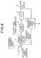
- a signal 2 indicating a reference frequency f0 generated from a reference signal generator 1 is supplied as input to a phase comparator 3, and a signal 7 obtained by dividing output from a voltage control oscillator (VCO) 5 with a frequency divider circuit 6 is connected to another input terminal of a phase comparator 3 for comparison of the phases.
- Output 8 from a phase comparator 3 is supplied as input to a loop filter 4 and then connected to the VCO 5 to control the VCO, thus a feedback loop being completed.
- Frequency division ratio N of the frequency divider circuit 6 is programmable, so that it is possible to obtain output from the VCO as a synthesizer output of N x f0 due to convergence of the feedback loop.
- a loop filter fully intercepts a reference frequency component, so that a time required for convergence of a feedback loop is limited to a value corresponding to a cycle of the reference frequency or below. For this reason, a conventional type of feedback loop can not be applied as it is to a synthesizer which requires a relatively high switching time.
- a direct digital synthesizer as shown in Fig. 7 is available.
- a frequency setting circuit 10 programs a phase increment 11 for unit clock corresponding to a frequency to be generated, the phase increase 11 is supplied as input to a phase accumulator 12, and accumulation of phase for unit clock of a clock signal 23 from the clock generator 21 is computed.
- a cumulative phase 13 is supplied as input to a ROM in which a value of sinusoidal wave form corresponding to each phase is stored, and output from the ROM is connected to a D/A convertor 15 and provided as output as a sinusoidal wave 16 converted into analog voltage.
- Analog output 16 is voltage sampled at a clock cycle, so that the wave form is as shown in Fig. 8A and includes many harmonic components. So a required synthesizer output 18 having a wave form as shown in Fig. 8B is obtained after removing the higher harmonic components by inserting a low-pass filter (LPF) 17.
- LPF low-pass filter
- the DDS shown in Fig. 7 uses a logic section ( consisting of a phase accumulator and a ROM) and a D/A convertor to generate a signal, so that an operating speed of the DDS is limited by the two components above, and can hardly generate a relatively high frequency. Also, when trying to generate a relatively high frequency, the clock frequency must be made higher, which in turn makes power consumption in the logic circuit and the D/A convertor disadvantageously higher.
- a frequency synthesizer comprises a clock generating means, a frequency setting means in which a phase increment for unit clock corresponding to a frequency to be generated according to input of a frequency set value is programmed, a phase accumulator to obtain a phase accumulation value by adding a phase increment set by this frequency setting means to a phase accumulation value by 1 clock before, wave form referring means for providing amplitude data corresponding to a cumulated phase output from the phase accumulator, a D/A convertor which converts amplitude data from the wave form referring means to an analog signal, and a band-pass filter which outputs filtered signals over a band of analog signals from this D/A convertor.
- a frequency synthesizer comprises a clock generating means, frequency setting means in which a phase increment for unit clock corresponding to a frequency to be generated according to input of a frequency set value is programmed, a phase accumulator to obtain a phase accumulation value by adding a phase increment set by this frequency setting means to a phase accumulation value by 1 clock before, wave form referring means for providing amplitude data corresponding to a cumulated phase output from the phase accumulator, a frequency divider which divides a clock from the clock generating means into two halves, a D/A convertor which inputs amplitude data from the wave form referring means and divided output from the frequency divider, converts the amplitude data into an analog signal, and inverts the polarity of output for each clock cycle according to the logic of the divided output, and a filter which passes, of components of an analog signal from the D/A converter, only frequency components higher than 1/2 of the clock frequency.
- a frequency synthesizer comprises, clock generating means, frequency setting means in which a phase increment for unit clock corresponding to a frequency to be generated according to input of a frequency set value is programmed, a phase accumulator to obtain a phase accumulation value by adding a phase increment set by this frequency setting means to a phase accumulation value by 1 clock before, a wave form referring means for providing amplitude data corresponding to a cumulated phase output from the phase accumulator, a D/C convertor which converts amplitude data from the wave form referring means to an analog signal, and a filter which passes, of components of an analog signal from the D/A converter, only frequency components higher than 1/2 of the clock frequency, wherein the most significant bit of the phase increment is "1".
- a frequency synthesizer comprises in addition to the components of the synthesizer above, a phase comparator, to one input terminal of which output from the filter is supplied as input, a loop filter into which output from the phase comparator is supplied as input, a voltage control oscillator which is controlled by output from this loop filter, and a frequency divider circuit which divides output from this voltage control oscillator and supplies the divided output to another input terminal of the phase comparator to form a feedback loop, wherein output from the voltage control oscillator is signal output.
- a feature of the present invention is that unnecessary frequency components generated by the DDS in Fig. 7 are positively utilized to generated a relatively high frequency.
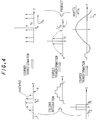
- Analog output underwent D/A conversion by the DDS in Fig. 7 can be expressed by the convolution integration as shown below (EXPRESSION 1) with assuming f0 as a clock frequency, T0 as the periodic time, and f s as a sinusoidal wave frequency to be generated:
- x(t) is a single pulse having a pulse width of T0.
- Fourier transformation of convolution integration is expressed by the product of Fourier transformation of each function for convolution integration. A wave form in a time domain and that in a frequency domain of each function are shown in Fig. 4.
- frequency components of nf0 + f s exist (n: an integral number). These frequencies can be programmed by the frequency setting circuit 10 in the DDS shown in Fig. 7 using the equation above.
- the maximum value of the frequency f s is 1/2 T0, and synthesizer output having a single frequency can be obtained by providing a band-pass filter which passes frequency components in a range from nf0 - f0/2 to nf0 or a band-pass filter which passes only frequency components in a range from nf0 to nf0 + f0/2 in the output side of the D/A convertor. Moreover, these frequencies are higher as compared to conventional ones.
- the synthesizer output thus obtained is advantageous in that a higher frequency can be obtained with the same power consumption as that in the conventional technology, but the output level is lower. Especially in an domain around nf0, amplitude comes closer to zero as clearly shown in Fig. 4, so that signal vs noise ratio (S/N) in the synthesizer output is sacrificed.
- polarity of output is inverted in each clock cycle when D/A conversion is executed.
- the D/A-converted output as shown in Fig. 5A can be obtained.
- This output signal has a wave form obtained by multiplying a sinusoidal wave having a frequency of f s with a continuous rectangular waves for each having a cycle of 1/2 T0.
- This spectrum is expressed by convolution integration for wave forms obtained by Fourier transformation of the sinusoidal wave and continuous rectangular waves respectively, and has frequency components of nf0/2 + fs (n: odd number) as shown in Fig. 5B.
- synthesizer output can be obtained by connecting a band-pass filter which passes only frequency components in a range from nf0/2 - f0/2 to nf0 (n: odd number) or a band-pass filter which passes only frequency components in a range from nf0 + f0/2 (n: odd number) behind the D/A convertor.
- the most significant bit in phase increment supplied to the phase accumulator 12 as an input may be set to "1".
- the DDS according to the present invention is used as a reference frequency signal source based on a feedback loop or so-called PLL realized by phase comparison for the purpose to generate signals having a higher frequency than that generated by the synthesizers described above.
- the PLL switching time largely depends on characteristics of a loop filter in a feedback loop, and this is largely affected by a reference frequency. Namely a shorter switching time as compared to that for a conventional type of PLL can be realized by using a relatively higher frequency generated by the DDS according to the present invention as a reference frequency.
- a frequency generated by this frequency synthesizer is decided by a set frequency for the DDS and a frequency division ratio by a feedback loop frequency divider, so that a very wide range of frequencies can be generated.
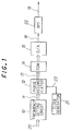
- Fig. 1 is a block diagram illustrating configuration of a frequency synthesizer according to the present invention, wherein a band-pass filter (BPF) 22 is used in place of a conventional type of DDS low pass filter 17 as shown in Fig. 7.
- BPF band-pass filter
- the same reference numerals are assigned to the same components as those in Fig. 7.
- frequency components of nf0 + f s in a spectrum of output frequency from a D/A convertor 15 exist, in addition to frequency components generally output in association with the frequency f s , frequency components of nf0 + f s (n: integral number).
- synthesizer output having a single frequency of nf0 - f s or nf0 + f s can be obtained by using a bandpass filter which passes only frequency components from nf0 - f0/2 to nf0 or a band-pass filter which passes only frequency components from nf0 to f0 + f0/2 in a band-pass filter 22.
- a frequency set value input 20 is supplied as input to the frequency setting circuit 10 to program phase increment 11 for unit clock corresponding to a frequency to be generated, and the phase increment 11 is supplied as input to the phase accumulator 12 to obtain accumulation of phases for each unit clock.
- the phase increment for unit clock is a value expressed by 2 ⁇ f s T0 .
- the clock signal 23 is generated by the clock generator 21 and supplied as input to the phase accumulator 12.
- the cumulative phase 13 is supplied as input to the ROM 14 in which a value of sinusoidal wave form corresponding to each phase is stored, and output from the ROM is connected to the D/A convertor and provided as output as the signal 16 converted into analog voltage.
- Signals from the frequency setting circuit 10 to the D/A convertor 15 are digital signals each consisting of a plurality of bits. For the necessity to process signals at a high speed, these digital signals are generally transferred in parallel through a plurality of lines.
- Analog output 16 is connected to the band-pass filter 22, which outputs a sinusoidal wave signal 18 having a single frequency component.
- Fig. 2 is a block diagram illustrating an embodiment of the present invention wherein the polarity of output from a D/A converted is inverted in each clock cycle.
- the frequency setting circuit 10, phase accumulator 12, clock generator 21, and ROM 14 are the same as those shown in Fig. 1.
- the frequency synthesizer according to this embodiment of the present invention includes the frequency divider circuit 24 which divides output from the clock generator 21 into two halves and supplied a clock signal divided into two halves to the D/A convertor 25.
- a band-pass filter 26 which passes only frequency components from nf0/2 - f0/2 to nf0 (n:odd number) or a band-pass filter which passes only frequency components from nf0 to nf0/2 + f0/2 (n:odd number) is used.
- the same effect can be achieved by setting the most significant bit of phase increment supplied to "input" to the phase accumulator 12 as "1" without inverting polarity of the output in each clock cycle when executing D/A conversion.
- the most significant bit of phase increment is set to "1".
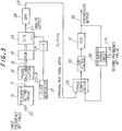
- Fig. 3 is a block diagram illustrating an embodiment of the present invention in which a conventional type of frequency synthesizer as shown in Fig. 6 is connected to the DDS shown in Fig. 2.
- a phase comparator 29, a loop filter 30, a VCO 31, and a 1/N frequency divider circuit are inserted behind the band-pass filter 26.
- a first frequency set value 33 is supplied as input to the frequency setting circuit 10, and a second frequency set value 34 is supplied as input to a frequency divider circuit 32.
- a sinusoidal wave signal output 28 of f0/2 + f s from the band-pass filter 26 described in relation to the embodiment of the present invention shown in Fig. 2 is connected as a reference frequency signal source to the phase comparator 29.
- a signal obtained by dividing output from the VCO 31 by N with the frequency divider 32 is supplied as input to another input terminal of the phase comparator 29.
- Output from the phase comparator is supplied as input to the loop filter 30 and then connected to the VCO to form a feedback loop.
- a frequency division ratio N in the frequency divider circuit 32 can be programmed according to a second frequency set value input 34, and the VCO 31 outputs a frequency of N x (f0/2 + f s ) as a synthesizer output 35.
- the synthesizer shown in Fig. 6 is connected to the DDS shown in Fig. 2, but also the synthesizer shown in Fig. 6 can be connected to the DDS shown in Fig. 1.
- the present invention advantageously provides a synthesizer which is based on a relatively simple circuit configuration, yet can switch a frequency at a high speed. Also the synthesizer can generate a wide range of frequencies without losing the advantage described above, when it is necessary to generate an extremely high frequency.
Landscapes
- Engineering & Computer Science (AREA)
- Theoretical Computer Science (AREA)
- Physics & Mathematics (AREA)
- General Engineering & Computer Science (AREA)
- General Physics & Mathematics (AREA)
- Stabilization Of Oscillater, Synchronisation, Frequency Synthesizers (AREA)
Applications Claiming Priority (2)
| Application Number | Priority Date | Filing Date | Title |
|---|---|---|---|
| JP4327781A JPH06177651A (ja) | 1992-12-08 | 1992-12-08 | 周波数シンセサイザ |
| JP327781/92 | 1992-12-08 |
Publications (3)
| Publication Number | Publication Date |
|---|---|
| EP0601519A2 true EP0601519A2 (de) | 1994-06-15 |
| EP0601519A3 EP0601519A3 (de) | 1995-01-11 |
| EP0601519B1 EP0601519B1 (de) | 1998-02-04 |
Family
ID=18202914
Family Applications (1)
| Application Number | Title | Priority Date | Filing Date |
|---|---|---|---|
| EP93119635A Expired - Lifetime EP0601519B1 (de) | 1992-12-08 | 1993-12-06 | Frequenzsynthetisierer |
Country Status (4)
| Country | Link |
|---|---|
| US (1) | US5428308A (de) |
| EP (1) | EP0601519B1 (de) |
| JP (1) | JPH06177651A (de) |
| DE (1) | DE69316857T2 (de) |
Cited By (2)
| Publication number | Priority date | Publication date | Assignee | Title |
|---|---|---|---|---|
| WO2002037684A1 (de) * | 2000-10-24 | 2002-05-10 | Sz Testsysteme Ag | Programmierbarer frequenzgenerator |
| EP1213856A1 (de) * | 1998-07-10 | 2002-06-12 | QUALCOMM Incorporated | Verfahren und Gerät zum Senden und Empfangen von Hochgeschwindigkeitsdaten unter Verwendung von Kodeverteilmehrfachzugriffskanälen |
Families Citing this family (11)
| Publication number | Priority date | Publication date | Assignee | Title |
|---|---|---|---|---|
| US5604679A (en) * | 1994-10-17 | 1997-02-18 | Nomadic Technologies, Inc. | Signal generating device using direct digital synthesis |
| JP2836526B2 (ja) * | 1995-04-10 | 1998-12-14 | 日本電気株式会社 | 周波数シンセサイザ |
| US5519343A (en) * | 1995-07-10 | 1996-05-21 | Fluke Corporation | Two channel direct digital synthesizer with waveform memory interleaving circuit |
| US5742208A (en) * | 1996-09-06 | 1998-04-21 | Tektronix, Inc. | Signal generator for generating a jitter/wander output |
| DE19727810C1 (de) * | 1997-06-30 | 1999-02-18 | Siemens Ag | Hochfrequenz-Signalgenerator |
| US6219088B1 (en) * | 1998-11-03 | 2001-04-17 | Broadcom Corporation | NTSC interference rejection filter |
| EP1212671A1 (de) * | 1999-07-16 | 2002-06-12 | Advanced Testing Technologies, Inc. | Verfahren und vorrichtung zum erzeugen von spektrumreinen programmierbaren signale |
| JP3226906B2 (ja) * | 1999-09-24 | 2001-11-12 | 埼玉日本電気株式会社 | 局部発振信号供給方法およびその回路 |
| IT1320247B1 (it) * | 2000-07-21 | 2003-11-26 | Gambro Dasco Spa | Metodo e dispositivo di impostazione di un trattamento dialitico inuna macchina per dialisi. |
| US20090086795A1 (en) * | 2007-09-28 | 2009-04-02 | Ahmadreza Rofougaran | Method and system for a low-complexity variable frequency oscillator using direct digital frequency synthesis |
| JP5424816B2 (ja) * | 2009-10-29 | 2014-02-26 | 三菱電機株式会社 | 周波数シンセサイザ |
Family Cites Families (5)
| Publication number | Priority date | Publication date | Assignee | Title |
|---|---|---|---|---|
| US4926130A (en) * | 1988-01-19 | 1990-05-15 | Qualcomm, Inc. | Synchronous up-conversion direct digital synthesizer |
| US4905177A (en) * | 1988-01-19 | 1990-02-27 | Qualcomm, Inc. | High resolution phase to sine amplitude conversion |
| US5028887A (en) * | 1989-08-31 | 1991-07-02 | Qualcomm, Inc. | Direct digital synthesizer driven phase lock loop frequency synthesizer with hard limiter |
| US4965533A (en) * | 1989-08-31 | 1990-10-23 | Qualcomm, Inc. | Direct digital synthesizer driven phase lock loop frequency synthesizer |
| US5081603A (en) * | 1990-04-02 | 1992-01-14 | Easton Corporation | Amplitude-control system for a signal generator |
-
1992
- 1992-12-08 JP JP4327781A patent/JPH06177651A/ja active Pending
-
1993
- 1993-12-06 DE DE69316857T patent/DE69316857T2/de not_active Expired - Fee Related
- 1993-12-06 EP EP93119635A patent/EP0601519B1/de not_active Expired - Lifetime
- 1993-12-08 US US08/162,982 patent/US5428308A/en not_active Expired - Lifetime
Cited By (5)
| Publication number | Priority date | Publication date | Assignee | Title |
|---|---|---|---|---|
| EP1213856A1 (de) * | 1998-07-10 | 2002-06-12 | QUALCOMM Incorporated | Verfahren und Gerät zum Senden und Empfangen von Hochgeschwindigkeitsdaten unter Verwendung von Kodeverteilmehrfachzugriffskanälen |
| US7675961B2 (en) | 1998-07-10 | 2010-03-09 | Qualcomm Incorporated | Method and apparatus for transmitting and receiving high speed data using code division multiple access channels |
| US8040936B2 (en) | 1998-07-10 | 2011-10-18 | Qualcomm, Incorporated | Method and apparatus for transmitting and receiving high speed data using code division multiple access channels |
| US8345728B2 (en) | 1998-07-10 | 2013-01-01 | Qualcomm Incorporated | Method and apparatus for transmitting and receiving high speed data using code division multiple access channels |
| WO2002037684A1 (de) * | 2000-10-24 | 2002-05-10 | Sz Testsysteme Ag | Programmierbarer frequenzgenerator |
Also Published As
| Publication number | Publication date |
|---|---|
| DE69316857T2 (de) | 1998-06-18 |
| JPH06177651A (ja) | 1994-06-24 |
| DE69316857D1 (de) | 1998-03-12 |
| EP0601519A3 (de) | 1995-01-11 |
| US5428308A (en) | 1995-06-27 |
| EP0601519B1 (de) | 1998-02-04 |
Similar Documents
| Publication | Publication Date | Title |
|---|---|---|
| US5093632A (en) | Latched accumulator fractional n synthesis with residual error reduction | |
| US7015733B2 (en) | Spread-spectrum clock generator using processing in the bitstream domain | |
| EP0601519A2 (de) | Frequenzsynthetisierer | |
| JP2004519917A (ja) | 改善されたノイズとスパー性能をもつσ−δn分周周波数分周器 | |
| EP0788237A1 (de) | Frequenzteiler mit rationalem teilerverhältnis und frequenzsynthetisierer damit | |
| JPWO1997006600A1 (ja) | ラショナル分周装置及びそれを用いる周波数シンセサイザ | |
| US7242225B2 (en) | Direct digital frequency synthesizer | |
| US7912882B2 (en) | Apparatus for generating clock pulses using a direct digital synthesizer | |
| US3995222A (en) | Sinusoidal waveform generator | |
| US4963839A (en) | Wide bandwidth phase locked loop circuit with sliding window averager | |
| US5673007A (en) | Frequency synthesizer having PLL receiving filtered output of DDS | |
| EP0378190A3 (de) | Digitale Phasenregelschleife | |
| JPH0645930A (ja) | 周波数シンセサイザ | |
| JP2000332539A (ja) | 周波数シンセサイザ | |
| JPH0548453A (ja) | 周波数シンセサイザ | |
| JP3797791B2 (ja) | Pllシンセサイザ発振器 | |
| SU794706A1 (ru) | Синтезатор частот | |
| RU2081510C1 (ru) | Синтезатор частот | |
| KR960012922B1 (ko) | 주파수 편이 키잉 변조기 | |
| SU1714785A2 (ru) | Формирователь случайных сигналов | |
| JP2907108B2 (ja) | 周波数合成回路 | |
| SU1681378A1 (ru) | Формирователь сложных сигналов | |
| RU8855U1 (ru) | Цифровой синтезатор частот | |
| Patel | Frequency Synthesizers and Their Applications in Signal Processing | |
| SU868973A1 (ru) | Синтезатор частот |
Legal Events
| Date | Code | Title | Description |
|---|---|---|---|
| PUAI | Public reference made under article 153(3) epc to a published international application that has entered the european phase |
Free format text: ORIGINAL CODE: 0009012 |
|
| AK | Designated contracting states |
Kind code of ref document: A2 Designated state(s): DE FR NL SE |
|
| PUAL | Search report despatched |
Free format text: ORIGINAL CODE: 0009013 |
|
| AK | Designated contracting states |
Kind code of ref document: A3 Designated state(s): DE FR NL SE |
|
| 17P | Request for examination filed |
Effective date: 19950307 |
|
| 17Q | First examination report despatched |
Effective date: 19960103 |
|
| RAP1 | Party data changed (applicant data changed or rights of an application transferred) |
Owner name: UNIDEN CORPORATION |
|
| GRAG | Despatch of communication of intention to grant |
Free format text: ORIGINAL CODE: EPIDOS AGRA |
|
| GRAG | Despatch of communication of intention to grant |
Free format text: ORIGINAL CODE: EPIDOS AGRA |
|
| GRAH | Despatch of communication of intention to grant a patent |
Free format text: ORIGINAL CODE: EPIDOS IGRA |
|
| GRAH | Despatch of communication of intention to grant a patent |
Free format text: ORIGINAL CODE: EPIDOS IGRA |
|
| GRAA | (expected) grant |
Free format text: ORIGINAL CODE: 0009210 |
|
| AK | Designated contracting states |
Kind code of ref document: B1 Designated state(s): DE FR NL SE |
|
| REF | Corresponds to: |
Ref document number: 69316857 Country of ref document: DE Date of ref document: 19980312 |
|
| ET | Fr: translation filed | ||
| PLBE | No opposition filed within time limit |
Free format text: ORIGINAL CODE: 0009261 |
|
| STAA | Information on the status of an ep patent application or granted ep patent |
Free format text: STATUS: NO OPPOSITION FILED WITHIN TIME LIMIT |
|
| 26N | No opposition filed | ||
| PGFP | Annual fee paid to national office [announced via postgrant information from national office to epo] |
Ref country code: SE Payment date: 20011217 Year of fee payment: 9 |
|
| PGFP | Annual fee paid to national office [announced via postgrant information from national office to epo] |
Ref country code: FR Payment date: 20011218 Year of fee payment: 9 Ref country code: DE Payment date: 20011218 Year of fee payment: 9 |
|
| PGFP | Annual fee paid to national office [announced via postgrant information from national office to epo] |
Ref country code: NL Payment date: 20011219 Year of fee payment: 9 |
|
| PG25 | Lapsed in a contracting state [announced via postgrant information from national office to epo] |
Ref country code: SE Free format text: LAPSE BECAUSE OF NON-PAYMENT OF DUE FEES Effective date: 20021207 |
|
| PG25 | Lapsed in a contracting state [announced via postgrant information from national office to epo] |
Ref country code: NL Free format text: LAPSE BECAUSE OF NON-PAYMENT OF DUE FEES Effective date: 20030701 Ref country code: DE Free format text: LAPSE BECAUSE OF NON-PAYMENT OF DUE FEES Effective date: 20030701 |
|
| EUG | Se: european patent has lapsed | ||
| NLV4 | Nl: lapsed or anulled due to non-payment of the annual fee |
Effective date: 20030701 |
|
| PG25 | Lapsed in a contracting state [announced via postgrant information from national office to epo] |
Ref country code: FR Free format text: LAPSE BECAUSE OF NON-PAYMENT OF DUE FEES Effective date: 20030901 |
|
| REG | Reference to a national code |
Ref country code: FR Ref legal event code: ST |