EP0788237A1 - Frequenzteiler mit rationalem teilerverhältnis und frequenzsynthetisierer damit - Google Patents
Frequenzteiler mit rationalem teilerverhältnis und frequenzsynthetisierer damit Download PDFInfo
- Publication number
- EP0788237A1 EP0788237A1 EP96925132A EP96925132A EP0788237A1 EP 0788237 A1 EP0788237 A1 EP 0788237A1 EP 96925132 A EP96925132 A EP 96925132A EP 96925132 A EP96925132 A EP 96925132A EP 0788237 A1 EP0788237 A1 EP 0788237A1
- Authority
- EP
- European Patent Office
- Prior art keywords
- value
- frequency
- integer
- output
- adder
- Prior art date
- Legal status (The legal status is an assumption and is not a legal conclusion. Google has not performed a legal analysis and makes no representation as to the accuracy of the status listed.)
- Withdrawn
Links
Images




Classifications
-
- G—PHYSICS
- G06—COMPUTING OR CALCULATING; COUNTING
- G06F—ELECTRIC DIGITAL DATA PROCESSING
- G06F7/00—Methods or arrangements for processing data by operating upon the order or content of the data handled
- G06F7/60—Methods or arrangements for performing computations using a digital non-denominational number representation, i.e. number representation without radix; Computing devices using combinations of denominational and non-denominational quantity representations, e.g. using difunction pulse trains, STEELE computers, phase computers
- G06F7/68—Methods or arrangements for performing computations using a digital non-denominational number representation, i.e. number representation without radix; Computing devices using combinations of denominational and non-denominational quantity representations, e.g. using difunction pulse trains, STEELE computers, phase computers using pulse rate multipliers or dividers pulse rate multipliers or dividers per se
-
- H—ELECTRICITY
- H03—ELECTRONIC CIRCUITRY
- H03L—AUTOMATIC CONTROL, STARTING, SYNCHRONISATION OR STABILISATION OF GENERATORS OF ELECTRONIC OSCILLATIONS OR PULSES
- H03L7/00—Automatic control of frequency or phase; Synchronisation
- H03L7/06—Automatic control of frequency or phase; Synchronisation using a reference signal applied to a frequency- or phase-locked loop
- H03L7/16—Indirect frequency synthesis, i.e. generating a desired one of a number of predetermined frequencies using a frequency- or phase-locked loop
- H03L7/18—Indirect frequency synthesis, i.e. generating a desired one of a number of predetermined frequencies using a frequency- or phase-locked loop using a frequency divider or counter in the loop
- H03L7/197—Indirect frequency synthesis, i.e. generating a desired one of a number of predetermined frequencies using a frequency- or phase-locked loop using a frequency divider or counter in the loop a time difference being used for locking the loop, the counter counting between numbers which are variable in time or the frequency divider dividing by a factor variable in time, e.g. for obtaining fractional frequency division
- H03L7/1974—Indirect frequency synthesis, i.e. generating a desired one of a number of predetermined frequencies using a frequency- or phase-locked loop using a frequency divider or counter in the loop a time difference being used for locking the loop, the counter counting between numbers which are variable in time or the frequency divider dividing by a factor variable in time, e.g. for obtaining fractional frequency division for fractional frequency division
- H03L7/1976—Indirect frequency synthesis, i.e. generating a desired one of a number of predetermined frequencies using a frequency- or phase-locked loop using a frequency divider or counter in the loop a time difference being used for locking the loop, the counter counting between numbers which are variable in time or the frequency divider dividing by a factor variable in time, e.g. for obtaining fractional frequency division for fractional frequency division using a phase accumulator for controlling the counter or frequency divider
Definitions
- the present invention relates to a rational number (rational) frequency division device and a frequency synthesizer using the same and, more particularly, to a rational frequency division device that can input an arbitrary rational number value and a frequency synthesizer that can output an output frequency signal corresponding to a non-integer multiple of a reference frequency with low spurious level using the rational frequency division device.
- a frequency synthesizer using a phase locked loop (PLL) circuit has a basic arrangement, as shown in FIG. 13 (note that the frequency division ratio to be input to a frequency divider 6 is only N (N: an integer)).
- a reference frequency signal a having a reference frequency f ref input from an input terminal 1 is input to a phase detector 2.
- the phase detector 2 detects the phase difference between the reference frequency signal a and a frequency-divided signal b output from the frequency divider 6, and outputs a phase difference signal c having a voltage proportional to the phase difference.
- phase difference signal c output from the phase detector 2 is input to a loop filter 3 to remove its high-frequency component, and thereafter, is input as a new phase difference signal c 1 to a voltage-controlled oscillator (VCO) 4.
- VCO voltage-controlled oscillator
- the VCO 4 outputs an output frequency signal d having an output frequency f out corresponding to the signal value of the phase difference signal c 1 to an output terminal 5.
- the output frequency signal d output from the VCO 4 is input to the frequency divider 6.
- the frequency divider 6 divides the frequency of the output frequency signal d by an externally input frequency division ratio N (N: an integer), and supplies the result to the phase detector 2 as the frequency-divided signal b.
- the output frequency f out of the basic arrangement of the frequency synthesizer using the PLL circuit, as shown in FIG. 13, can only assume values corresponding to integer multiples of the reference frequency f ref .
- the frequency division ratio to be set in the frequency divider 6 in the frequency synthesizer using the PLL circuit, as shown in FIG. 13, is switched from N to (N+1) at predetermined periods, as shown in FIG. 14.
- the output frequency f out as a whole assumes a value not N times but [N.1] times the reference frequency f ref .
- N is an integer value
- J is a decimal value (a value below the decimal point) called a fractional value.
- a modulation signal e having a frequency f m may be applied from an input terminal 8 to the input stage of the VCO 4 via a signal multiplexer 7, as shown in FIG. 15.
- a voltage obtained by integrating a modulation wave on the output from the phase detector 2 by an integrator 9 may be applied.
- phase difference signal c (c 1 ) mixed with periodic phase difference errors is input to the VCO 4
- fractional spurious components that are hard to remove are generated in the neighborhood of the carrier frequency in the output frequency signal d output from the VCO 4.
- FIG. 3A shows the instantaneous value of the decimal part of the frequency division ratio (N, N+1) set in the frequency divider 6.
- FIG. 4A shows phase errors E between the reference frequency signal a at the input stage of the phase detector 2, and the frequency-divided signal c.
- phase errors E are superposed on the phase difference signal c, and the superposed signal is input to the VCO 4.
- FIG. 5 shows the spurious level with respect to an offset frequency f OFF from the carrier frequency, which is plotted along the abscissa.
- the characteristic values shown in FIGS. 3A, 4A, and 5 are obtained by calculating, by a simulation method, the operation of the frequency synthesizer that adopts the fractional N scheme shown in FIG. 13, when the clock frequency is set to be 500 kHz, and the rate of replacing the frequency division ratio N by the frequency division ratio (N+1) is set to be once in a thousand times.
- Each modulation circuit 17 is constituted by a cumulative adder 17a for cumulating the decimal value J in synchronism with a clock signal CLK input from a clock terminal 18, and outputting an overflow signal when the cumulative value has exceeded a value [1], an adder 17b, and a differentiator 17c.
- the decimal value J to be applied to the arithmetic circuit 15 need only be changed to (J + ⁇ J).
- the modulation width is limited in association with the integer value N or another measure must be taken to avoid it.
- the frequency synthesizer adopting the multiple modulator fractional N scheme shown in FIG. 16 includes structural spurious components.
- phase errors E in the phase detector 2 have only patterns with short periods, as shown in FIG. 3A.
- Jpn. Pat. Appln. KOKAI Publication No. 2-198224 discloses a technique nearly equivalent to United States Patent No. 4,546,331 above.
- Jpn. Pat. Appln. KOKAI Publication No. 2-198224 does not particularly refer to frequency modulation, but this technique is speculated to be free from the inconvenience in United States Patent No. 4,546,331.
- the conventional frequency synthesizers commonly have the following problems although they have both merits and demerits.
- the present invention has been made in consideration of the above situation, and has as its object to provide a rational frequency division device which can suppress fractional spurious components by a simple arrangement, can assure a broad frequency modulation range, and can easily reduce structural spurious components, since an arithmetic circuit for calculating the frequency division value to be set in a frequency divider has an arrangement that allows easy cascade connection of a plurality of cumulative adders, which are used in the arithmetic circuit and perform calculations in a rational number state including integer and decimal values, and a frequency synthesizer using the same.
- a frequency synthesizer comprising a variable frequency oscillator for outputting a frequency signal having a frequency corresponding to an input signal, a frequency divider for frequency-dividing the frequency of the output frequency signal output from the variable frequency oscillator by an integer frequency division ratio applied, a phase detector for detecting a phase difference between a reference frequency signal and a frequency-divided signal output from the frequency divider, and outputting a phase difference signal corresponding to the phase difference to the variable frequency oscillator, and an arithmetic circuit for calculating a frequency division ratio, which becomes an input rational number defined by an integer value and a decimal value if an average value is calculated and is indicated by an integer value that changes instantaneously, upon receiving the rational value, and outputting the frequency division ratio to the frequency divider, wherein the arithmetic circuit has a plurality of cumulative adders which include a first cumulative adder that receives the rational number and are series-connected, an integer value extraction circuit for extracting an integer
- a rational frequency division device comprising a frequency divider for frequency-dividing a frequency of an input frequency signal by an integer frequency division ratio applied, and an arithmetic circuit for calculating a frequency division ratio, which becomes an input rational number defined by an integer value and a decimal value if an average value is calculated and is indicated by an integer value that changes instantaneously, upon receiving the rational value, and outputting the frequency division ratio to the frequency divider, wherein the arithmetic circuit has a plurality of cumulative adders which include a first cumulative adder that receives the rational number and are series-connected, an integer value extraction circuit for extracting an integer value from an output value of the cumulative adder of a final stage, and a delay circuit for outputting the integer value extracted by the integer value extraction circuit to the frequency divider as the frequency division ratio, and outputting the integer value to the cumulative adders as a feedback value, and each of the cumulative adders adds a value calculated by itself in a previous clock period to the input rational number
- a frequency synthesizer comprising a variable frequency oscillator for outputting a frequency signal having a frequency corresponding to an input signal, a frequency divider for frequency-dividing the frequency of the output frequency signal output from the variable frequency oscillator by an integer frequency division ratio applied, a phase detector for detecting a phase difference between a reference frequency signal and a frequency-divided signal output from the frequency divider, and outputting a phase difference signal corresponding to the phase difference to the variable frequency oscillator, and an arithmetic circuit for supplying an integer frequency division signal to the frequency divider upon receiving an input rational number (K) defined by an integer value (I) and a decimal value (J), characterized in that the arithmetic circuit includes a plurality of cumulative adders which are cascade-connected in at least three stages and have an integral function, and outputs the integer frequency division signal ( ⁇ k) on the basis of the rational number (K) defined by the integer value (I) and the decimal value (J
- a rational frequency division device comprising a frequency divider for frequency-dividing a frequency of an input frequency signal by an integer frequency division ratio applied, and an arithmetic circuit for supplying an integer frequency division signal to the frequency divider upon receiving an input rational number (K) defined by an integer value (I) and a decimal value (J), characterized in that the arithmetic circuit includes a plurality of cumulative adders which are cascade-connected in at least three stages and have an integral function, and outputs the integer frequency division signal ( ⁇ k) on the basis of the rational number (K) defined by the integer value (I) and the decimal value (J).
- a frequency synthesizer comprising a variable oscillator, a frequency divider for frequency-dividing a frequency signal from the variable oscillator by an integer frequency division ratio in correspondence with a setting value, a phase detector for detecting a phase difference between a reference signal and a frequency-divided signal from the frequency divider, and outputting a phase difference signal corresponding to the phase difference to the variable oscillator, and an arithmetic circuit which has a plurality of (n) integrators which are cascade-connected in at least three stages, performs a calculation upon receiving a rational number (I,J) defined by an integer value (I) and a decimal value (J), and sets the calculation result in the frequency divider, so that the frequency-divided signal output from the frequency divider includes a rational number frequency component if an average value is calculated, and an error frequency component which decreases toward a low-frequency region at a gradient of about 6 ⁇ n (dB/octa
- the loop attenuation characteristics of a PLL circuit itself constituted by a closed loop of a phase detector, a variable frequency oscillator, and a frequency divider can sufficiently attenuate noise and spurious components having frequencies at positions sufficiently separated from the carrier frequency of an output frequency signal to be output from the variable frequency oscillator to an external circuit.
- an arithmetic circuit for sequentially calculating frequency division ratios to be applied in turn to the frequency divider uses a plurality of cascade-connected cumulative adders to provide differential characteristics with respect to the switching characteristics of the frequency division ratio for the frequency divider, and an integer value extraction circuit extracts only an integer value by rounding off a decimal value from the output value of the cumulative adder. The extracted integer value is used as the frequency division ratio, and the frequency division ratio is delayed and fed back to each cumulative adder.
- the generation periods of instantaneous phase errors generated between the reference frequency signal input to the phase detector and the frequency-divided signal output from the frequency divider are not uniform but are dispersed to be lower than the Nyquist frequency.
- spurious components in the neighborhood of the carrier attenuate by the differential characteristics. In this way, spurious components appearing in the output frequency signal owing to the phase errors outside the frequency band are attenuated by the loop attenuation characteristics of the PLL circuit itself, thus obtaining an output signal with low spurious level over the entire frequency band.
- the arithmetic circuit since the arithmetic circuit has an arrangement that can cumulate the entire input rational number, when the output frequency signal is to be frequency-modulated, modulation can be made for the entire rational number to be applied to the arithmetic circuit, and the modulation width in this case can be set for the entire rational number obtained by adding integer and decimal values.
- the modulation width can be set to be an arbitrary value.
- the average frequency division ratio that frequency-divides the frequency of the input frequency signal can be consequently set to be not only an integer value but also a rational number defined by integer and decimal values.
- the frequency of the input frequency signal can be converted into an arbitrary frequency.
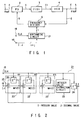
- FIG. 1 is a schematic block diagram showing the arrangement of a rational frequency division device and a frequency synthesizer using the same according to the first embodiment of the present invention.
- FIG. 1 denotes the same parts as in the conventional frequency synthesizers shown in FIGS. 13 and 16, and a detailed description of repetitive portions will be omitted.
- a reference frequency signal a having a reference frequency f ref input from an input terminal 1 is input to a phase detector 2.
- the phase detector 2 detects the phase difference between the reference frequency signal a and a frequency-divided signal b output from a frequency divider 6, and outputs a phase difference signal c having a voltage proportional to the phase difference.
- phase difference signal c output from the phase detector 2 is input to a loop filter 3 to remove its high-frequency component, and thereafter, is input as a new phase difference signal c 1 to a VCO (voltage-controlled oscillator) 4 serving as a variable frequency oscillator.
- VCO voltage-controlled oscillator
- the VCO 4 outputs an output frequency signal d having an output frequency f out proportional to the signal value of the phase difference signal c 1 to an output terminal 5.
- the output frequency signal d output from the VCO 4 is input to the frequency divider 6.
- the frequency divider 6 frequency-divides the frequency of the output frequency signal d by an externally input frequency division ratio I (I: an integer) and applies the result as the frequency-divided signal b to the phase detector 2.
- the frequency division ratio I set in the frequency divider 6 is supplied from an arithmetic circuit 21.
- the arithmetic circuit 21 receives a rational number value [I.J] via an input terminal 16.
- the rational number value [I.J] is defined by an i-bit integer value I and a j-bit decimal value J called a fractional value.
- the arithmetic circuit 21 receives a clock signal CLK from an input terminal 18.
- the arithmetic circuit 21 constitutes a rational frequency division device together with the frequency divider 6, and applies an i-bit arithmetic result as the frequency division ratio I to the frequency divider 6.
- the arithmetic circuit 21 is constituted by n (n ⁇ 3) cascade-connected cumulative adders 22, an integer value extraction circuit 23 for extracting an integer value I from a sum value consisting of a rational number value output from the final-stage (n-th) cumulative adder 22, and a delay circuit 24 for delaying the integer value I extracted by the integer value extraction circuit 23 by one clock period T 0 .
- the i-bit integer value I output from the delay circuit 24 is output to the frequency divider 6, and is also fed back to the respective cumulative adders 22 as a feedback value.
- the cumulative adders 22, the integer value extraction circuit 23, and the delay circuit 24 are applied with the clock signal CLK input from the input terminal 18.
- the adder 25 also receives the sum obtained by delaying the sum by one clock period T 0 by a delay circuit 26.
- each cumulative adder 22 adds the output value in the previous clock period to the rational number value input from the cumulative adder 22 of the previous stage, also adds the sum in the previous clock period, and outputs the sum to the cumulative adder 22 of the next stage.
- M 1 (z), ⁇ , M n (z) represent the sums of the adders 25 in the first to n-th cumulative adders 22 in the arithmetic circuit 21, these sums M 1 (z), M 2 (z), ⁇ , M n (z) are respectively given by the following equations:
- ⁇ I(z) in equation (5) represents errors generated by extracting only an integer value I(z) and rounding off a decimal value J(z) (lower bits) by the integer value extraction circuit 23 from the sum value as a rational number output from the adder 25 of the final-stage (n-th stage) cumulative adder 22.
- equation (5) amounts to adding an error ⁇ I(z) between the average value and instantaneous value of the frequency-divided signal b output from the frequency divider 6 to the integer value I(z) applied to the frequency divider 6 in the PLL circuit.
- the output frequency f out of the output frequency signal d is defined by the frequency components ⁇ [I.J]f ref ) ⁇ corresponding to rational number multiples of the reference frequency f ref and spurious components ⁇ (1 - z -1 ) n ⁇ I(z)f ref ⁇ produced due to phase errors (phase jitter).
- spurious components have differential characteristics (1 - z -1 ) n having the same order n as the number of setting stages of the cumulative adders 22.
- the order n can be stably increased by increasing the number n of setting stages of the cumulative adders 22 without being saturated.
- the noise shaping effect based on the number n of setting stages of the cumulative adders 22 is 6 ⁇ n (dB/octave), and tends to lower in the low-frequency region.
- This noise shaping effect can be demonstrated by executing simulation arithmetic operations using a sequence in the time domain.
- INT max ⁇ S 3 (k) ⁇ in equation (15) represents a maximum integer value equal to or smaller than S 3 (k).
- S(k+1) represents the state of the output value S(k) after an elapse of one clock period T 0 .
- equation (18) is uniquely determined by giving the initial value of S 3 (k), an instantaneous value (error) ⁇ I(k) of a frequency division ratio I(k) to be set in the frequency divider 6 is obtained from equation (15).
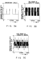
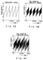
- FIGS. 3B and 3C, FIGS. 4B and 4C, and FIGS. 6 and 7 are graphs showing the operations of the frequency synthesizer of the first embodiment shown in FIGS. 1 and 2 calculated by the above-mentioned simulation arithmetic operations.
- the detailed conditions in this case are the same as the simulation conditions of the conventional frequency synthesizer shown in FIGS. 3A, 4A, and 5.
- the clock frequency of the clock signal CLK is set to be 500 kHz, and the decimal value J of the rational number [I.J] is set to be 0.001.
- simulation arithmetic operations were conducted in correspondence with cases including two and three stages of cumulative adders 22.
- FIGS. 3A, 3B, and 3C show the instantaneous values of the decimal part of the frequency division ratio set in the frequency divider 6 in the case of the conventional synthesizer (FIG. 3A), the case of the two stages in this embodiment (FIG. 3B), and the case of the three stages in this embodiment (FIG. 3C).
- the characteristics of the conventional apparatus have given periodicity, but the characteristics (FIGS. 3B and 3C) of this embodiment have weaker periodicities as the number of stages of the cumulative adders 22 is larger.
- FIGS. 4A, 4B, and 4C show the phase errors E between the reference frequency a and the frequency-divided signal c at the input stage of the phase detector 2 in the case of the conventional synthesizer (FIG. 4A), the case of the two stages in this embodiment (FIG. 4B), and the case of the three stages in this embodiment (FIG. 4C).
- the characteristics of the conventional apparatus are defined by a periodic, typical sawtooth waveform, but the waveform deforms and the periodicity weakens in the characteristics of this embodiment (FIGS. 4B and 4C) as the number of stages of the cumulative adders 22 is larger.
- FIGS. 5, 6, and 7 show the spurious levels with respect to the offset frequency f OFF from the carrier frequency, which is plotted along the abscissa, in the case of the conventional synthesizer (FIG. 5), the case of the two stages in this embodiment (FIG. 6), and the case of the three stages in this embodiment (FIG. 7).
- spurious components present at frequencies sufficiently separated from the carrier can be attenuated by the attenuation characteristics of the PLL circuit, a low-spurious output frequency signal d can be obtained in the whole frequency band.
- the conventional apparatus can only reduce the spurious level to about -70 dB, but this embodiment using the three stages of cumulative adders 22 can reduce the spurious level to -100 dB or less.
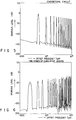
- FIGS. 8A and 8B show the simulation calculation results of the spurious characteristics included in the output frequency signal d when five stages of cumulative adders 22 are used in the frequency synthesizer of the first embodiment shown in FIGS. 1 and 2.
- the characteristics indicated by the solid curve in FIG. 8A represent the spurious characteristics when the high-frequency attenuation function of the PLL circuit itself is not taken into consideration.
- the characteristics indicated by the solid curve in FIG. 8B represent the spurious characteristics closer to those of an actual PLL circuit when the high-frequency attenuation function of the PLL circuit itself is taken into consideration.
- a dotted curve in FIG. 8B represents the attenuation characteristics of the PLL circuit including the loop filter 3 as well.
- frequency modulation of the output frequency signal d is attained by modulating the entire rational number [I.J] to be applied to the arithmetic circuit 21.
- the entire rational number [I.J + ⁇ I.J] is input to the arithmetic circuit 21, and the respective cumulative adders 22 execute arithmetic operations for the entire [I.J + ⁇ I.J].
- the integer value extraction circuit 23 extracts an integer value from the sum of the rational number, and outputs it to the frequency divider 6.
- the value to be finally input to the frequency divider 6 need only satisfy the integer value condition, and need not satisfy the condition of (J + ⁇ J) ⁇ [1] unlike in the conventional multiple-modulator fractional N type frequency synthesizer shown in FIG. 16.
- the frequency shift width ⁇ I.J max is not limited by the value J.
- a modulation width ⁇ I.J can be set to an arbitrary value.
- the frequency range of the modulation frequency is not particularly limited, and frequency modulation is allowed within a low-frequency region from the direct current (DC) region to the cut-off frequency f c of the loop frequency of the PLL circuit.
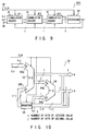
- FIG. 9 is a schematic block diagram showing the arrangement of an arithmetic circuit 21a built in a frequency synthesizer according to the second embodiment of the present invention.
- this frequency synthesizer Since the overall arrangement of this frequency synthesizer is the same as that of the frequency synthesizer of the first embodiment shown in FIG. 1, a detailed description of repetitive portions will be omitted.
- the arithmetic circuit 21a in this frequency synthesizer is constituted by n stages of cascade-connected cumulative adders 31 and a register 32.
- a rational number [I,J] input from an input terminal 16 is input to the first cumulative adder 31 in the arithmetic circuit 21a.
- the rational number [I,J] input to the arithmetic circuit 21a is defined by an i-bit integer value I and a j-bit decimal value J.
- the respective cumulative adders 31 and the register 32 in the arithmetic circuit 21a are applied with a clock signal CLK input via an input terminal 18.
- the register 32 Upon receiving one clock signal CLK, the register 32 fetches and holds an upper i-bit integer value I from an (i+j)-bit rational number [I,J] output from the final-stage (n-th) cumulative adder 31.
- the register 32 Upon receiving the next clock signal CLK, the register 32 outputs the held i-bit integer value I to a frequency divider 6 as a frequency division ratio, and also outputs this integer value I to the respective cumulative adders 31 as a feedback value.
- the register 32 constitutes an integer value extraction circuit for extracting an integer value from the sum value of the final-stage (n-th) cumulative adder 31 and a delay circuit for delaying the extracted integer value by one clock period T 0 .
- Each cumulative adder 31 in the arithmetic circuit 21a is constituted by an adder 33, a subtracter 34, and a register 35, as shown in FIG. 10.
- an (i+j)-bit rational number [I,J] output from the cumulative adder 31 of the previous stage is input to one input terminal 33a of the adder 33.
- the other input terminal 33b of the adder 33 receives an (i+j)-bit rational number [I,J] output from the register 35 serving as an intra-circuit delay circuit.
- the adder 33 adds the rational numbers input from the input terminals 33a and 33b in synchronism with the clock signal CLK, and outputs an (i+j)-bit sum value.
- An upper i-bit integer value of the sum value output from the adder 33 is applied to one input terminal 34a of the subtracter 34.
- the other input terminal 34b of the subtracter 34 receives the i-bit integer value I output from the register 32 shown in FIG. 9 as a feedback value.
- the subtracter 34 subtracts the integer value input to the input terminal 34b from the integer value input to the input terminal 34a in synchronism with the clock signal CLK, and outputs an i-bit difference value.
- a lower j-bit decimal value J of the sum value output from the adder 33 and the i-bit integer value output from the subtracter 34 are synthesized, and the synthesized value is output as the sum value of the (i+j)-bit rational number [I,J] to the cumulative adder 31 of the next stage.
- the (i+j)-bit rational number [I,J] is also input to the register 35.
- the register 35 delays the input (i+j)-bit rational number [I,J] by one clock period T 0 , and outputs the delayed value to the input terminal 33b of the adder 33.
- the cumulative adder 31 constituted by a plurality of digital operational elements adds its own sum result in the previous clock period to the sum result of the previous cumulative adder 31, and subtracts the integer value to be output to the frequency divider 6 therefrom, as in each cumulative adder 31 in the first embodiment shown in FIG. 2.
- the arithmetic circuit 21a shown in FIG. 9 performs the same arithmetic processing operation as that of the arithmetic circuit 21 of the first embodiment shown in FIG. 2.
- the frequency synthesizer of the second embodiment can provide substantially the same technical effects as those of the frequency synthesizer of the first embodiment shown in FIGS. 1 and 2.
- FIG. 11 is a schematic block diagram showing the arrangement of an arithmetic circuit 21b built in a frequency synthesizer according to the third embodiment of the present invention.
- this frequency synthesizer Since the overall arrangement of this frequency synthesizer is the same as that of the frequency synthesizer of the first embodiment shown in FIG. 1, a detailed description of repetitive portions will be omitted.
- An i-bit integer value I output from the integer value extraction circuit 23 in the arithmetic circuit 21b is output to a frequency divider 6 as the arithmetic operation result, and is also fed back to the respective cumulative adders 36 in the arithmetic circuit 21b.
- the respective cumulative adders 36 and the integer value extraction circuit 23 in the arithmetic circuit 21b are applied with a clock signal CLK input from an input terminal 18.
- Each cumulative adder 36 in the arithmetic circuit 21b is constituted by an adder 25, a delay circuit 26a, and a multiplier 37.
- the multiplier ⁇ of the first cumulative adder 36 is 1, and the multiplier ⁇ 1 of the second cumulative adder 36 is 3.
- multiplier ⁇ 2 of the third (final stage) cumulative adder 36 is 3.
- the multiplier ⁇ of the first cumulative adder 36 is 1, and the multiplier ⁇ 1 of the second cumulative adder 36 is 4.
- multiplier ⁇ 2 of the third cumulative adder 36 is 6, and the multiplier ⁇ 3 of the fourth (final stage) cumulative adder 36 is 4.
- the adder 25 in each cumulative adder 36 receives the sum value of the cumulative adder 36 of the previous stage, its own sum result in the previous clock period T 0 delayed by the delay circuit 26a, and an integer value obtained by multiplying the integer value to be output to the frequency divider 6 with the multiplier ⁇ .
- each cumulative adder 36 in the arithmetic circuit 21b performs substraction between a value obtained by adding the output value in the nth previous clock period to the rational number input from the cumulative adder 36 of the previous stage, and multiplying the sum with ⁇ , and the sum value in the previous clock period, and outputs the calculated value to the cumulative adder 36 of the next stage.
- f out (z) (z -1 ) n [I.J]f ref + (1 - z -1 ) n ⁇ I(z)f ref
- the frequency synthesizer of the third embodiment can obtain substantially the same frequency characteristics as those of the frequency synthesizer of the first embodiment having the arithmetic circuit 21 shown in FIG. 2, except that the frequency multiplied with the rational number [I.J] is output while being delayed by a time n times the clock period T 0 .
- the total arithmetic time of the n stages of cumulative adders 22 required from when the rational number is input to the first cumulative adder 22 until the sum value is output from the cumulative adder 22 of the final stage must fall within one clock period T 0 .
- the arithmetic time required from when the sum value from the cumulative adder 36 of the previous stage is input until the sum value is output to the cumulative adder 36 of the next stage after predetermined addition/subtraction need only fall within one clock period T 0 .
- the frequency synthesizer of the third embodiment can increase the processing speed of the entire apparatus by shortening the clock period T 0 of the clock signal CLK.
- FIG. 12 is a schematic block diagram showing the arrangement of each of n stages of cumulative adders that constitute an arithmetic circuit built in a frequency synthesizer according to the fourth embodiment of the present invention.
- a register 32 is built in after the cumulative adder 41 of the final stage as in the arithmetic circuit 21b of the second embodiment shown in FIG. 9.
- FIG. 12 denote the same parts as in the cumulative adder 31 shown in FIG. 10, and a detailed description of repetitive portions will be omitted.
- each cumulative adder 41 of the fourth embodiment the register 35 inserted in the feedback path of the cumulative adder 31 shown in FIG. 10 is removed, and a common register 39 is inserted at the output stage of an adder 33 and the output stage of a subtracter 34.
- the register 39 in each cumulative adder 41 has a function of delaying the output values from the adder 33 and the subtracter 34 by one clock period T 0 .
- each cumulative adder 41 in the fourth embodiment has the same operation and characteristics as those of the cumulative adder 36 in the arithmetic circuit 21b in the third embodiment shown in FIG. 11.
- an arithmetic circuit is essentially an arithmetic circuit (21, 21a, 21b) that gives an integer frequency-divided signal ( ⁇ k) to the frequency divider (6) upon receiving an input rational number (K) defined by an integer value (I) and a decimal value (J), includes a plurality of cumulative adders (22, 31, 36, 41) which are cascade-connected in at least three stages and have an integral function, and need only have a function of outputting the integer frequency-divided signal ( ⁇ k) on the basis of the rational number (K) defined by the integer value (I) and the decimal value (J).
- the frequency-divided signal ( ⁇ k) substantially satisfies the relation given by the following equation with respect to the rational number (K) defined by the integer value (I) and the decimal value (J):
- this essentially means that the arithmetic circuit (21, 21a, 21b) calculates the frequency division ratio, which becomes the rational number if the average value is calculated, and is indicated by an integer value that changes instantaneously, upon receiving the input rational number defined by the integer value and the decimal value, and outputs it to the frequency divider.
- the present invention is not limited to the first to fourth embodiments described above.
- the frequency synthesizer comprising the PLL circuit is constituted by a rational frequency division device consisting of the frequency divider 6 and the arithmetic circuit 21 (21a, 21b), the phase detector 2, the loop filter 3, and the VCO 4.
- the rational frequency division device can be used alone, or can be built in various other apparatuses other than the frequency synthesizer comprising the PLL circuit.
- the minimum resolution of the output frequency of a DDS (Direct digital synthesizer) using a 16-bit binary NCO (Numerically Controlled Oscillator) is Fclk/2 16 where Fclk is the clock frequency of the NCO.
- the clock signal has a frequency of 65.536 MHz
- a decimal output frequency having a minimum resolution of 1 kHz can be obtained.
- this clock signal when this clock signal is used as the reference signal of another decimal control circuit, it must be converted into a frequency of 10 MHz or the like.
- 65.536 MHz can be directly frequency-divided by 6.5536 and the frequency-divided signal is supplied to a band-pass filter to obtain a low-spurious 10-MHz output.
- the arithmetic circuit for calculating the frequency division value to be set in the frequency divider is constituted by cascade-connecting a plurality of cumulative adders that perform calculations in the rational number state including an integer value and a decimal value.
- fractional spurious components can be suppressed by a simple arrangement, and the frequency modulation range in the case of frequency-modulating an output frequency signal can be broadened.
- structural spurious components can be easily eliminated.
Landscapes
- Engineering & Computer Science (AREA)
- Physics & Mathematics (AREA)
- General Physics & Mathematics (AREA)
- Theoretical Computer Science (AREA)
- Computational Mathematics (AREA)
- Computing Systems (AREA)
- Mathematical Analysis (AREA)
- Mathematical Optimization (AREA)
- Mathematical Physics (AREA)
- Pure & Applied Mathematics (AREA)
- General Engineering & Computer Science (AREA)
- Stabilization Of Oscillater, Synchronisation, Frequency Synthesizers (AREA)
Applications Claiming Priority (3)
| Application Number | Priority Date | Filing Date | Title |
|---|---|---|---|
| JP198653/95 | 1995-08-03 | ||
| JP19865395 | 1995-08-03 | ||
| PCT/JP1996/002143 WO1997006600A1 (fr) | 1995-08-03 | 1996-07-30 | Diviseur rationnel de frequences et synthetiseur de frequences employant ce diviseur de frequences |
Publications (2)
| Publication Number | Publication Date |
|---|---|
| EP0788237A1 true EP0788237A1 (de) | 1997-08-06 |
| EP0788237A4 EP0788237A4 (de) | 1998-11-25 |
Family
ID=16394807
Family Applications (1)
| Application Number | Title | Priority Date | Filing Date |
|---|---|---|---|
| EP96925132A Withdrawn EP0788237A4 (de) | 1995-08-03 | 1996-07-30 | Frequenzteiler mit rationalem teilerverhältnis und frequenzsynthetisierer damit |
Country Status (4)
| Country | Link |
|---|---|
| US (1) | US5808493A (de) |
| EP (1) | EP0788237A4 (de) |
| JP (1) | JP3086706B2 (de) |
| WO (1) | WO1997006600A1 (de) |
Cited By (5)
| Publication number | Priority date | Publication date | Assignee | Title |
|---|---|---|---|---|
| WO1999031807A1 (en) * | 1997-12-12 | 1999-06-24 | Telefonaktiebolaget Lm Ericsson (Publ) | Σδ modulator-controlled phase-locked-loop circuit and associated method |
| EP1111793A1 (de) * | 1999-12-13 | 2001-06-27 | Matsushita Electric Industrial Co., Ltd. | Frequenzsynthetisierer mit gebrochenem Teilerverhältnis und Delta-Sigma Modulator zur Kontrolle des fraktionalen Teils |
| WO2002027936A3 (en) * | 2000-09-27 | 2003-01-09 | Hughes Electronics Corp | Feed forward sigma delta interpolator for use in a fractional-n synthesizer |
| WO2004042928A1 (de) * | 2002-11-06 | 2004-05-21 | Infineon Technologies Ag | Schaltungsanordnung zur frequenzteilung und phasenregelschleife mit der schaltungsanordnung |
| US9000858B2 (en) | 2012-04-25 | 2015-04-07 | Qualcomm Incorporated | Ultra-wide band frequency modulator |
Families Citing this family (20)
| Publication number | Priority date | Publication date | Assignee | Title |
|---|---|---|---|---|
| US6515526B2 (en) | 1999-04-26 | 2003-02-04 | Ando Electric Co., Ltd. | Phase fluctuation generation |
| US6581082B1 (en) * | 2000-02-22 | 2003-06-17 | Rockwell Collins | Reduced gate count differentiator |
| US6396313B1 (en) * | 2000-08-24 | 2002-05-28 | Teradyne, Inc. | Noise-shaped digital frequency synthesis |
| DE60125299T2 (de) * | 2000-09-29 | 2007-10-04 | Koninklijke Philips Electronics N.V. | Frequenzsynthesizer und Verfahren zur Frequenzsynthese mit geringem Rauschen |
| JP2002182898A (ja) * | 2000-12-14 | 2002-06-28 | Nec Microsystems Ltd | 積算値及び周期関数の生成方法及び回路 |
| DE60211460T2 (de) * | 2001-10-30 | 2006-12-21 | Stmicroelectronics Pvt. Ltd. | Volldigitale Taktrückgewinnung mit Teiler mit gebrochenem Teilungsverhältnis |
| US6917247B2 (en) * | 2002-04-26 | 2005-07-12 | Broadcom Corporation | NCO based timebase recovery system and method for A/V decoder |
| US6954114B2 (en) * | 2002-04-26 | 2005-10-11 | Broadcom Corporation | NCO with rational frequency and normalized phase |
| FR2845783A1 (fr) * | 2002-10-15 | 2004-04-16 | St Microelectronics Sa | Generateur d'horloge a consigne decimale et application d'un tel generateur d'horloge a un circuit uart |
| TWI245178B (en) * | 2004-01-16 | 2005-12-11 | Realtek Semiconductor Corp | Clock generation method and apparatus |
| WO2005071840A2 (en) * | 2004-01-21 | 2005-08-04 | Telefonaktiebolaget L M Ericsson (Publ) | Frequency generator with multiple voltage-controlled oscillators |
| KR100699080B1 (ko) * | 2004-09-22 | 2007-03-23 | 지씨티 세미컨덕터 인코포레이티드 | 광대역 주파수 발진 장치 및 그 방법 |
| DE102004047683B4 (de) * | 2004-09-30 | 2007-05-10 | Advanced Micro Devices, Inc., Sunnyvale | Niedrig-IF-Mehrfachmodus-Sender-Front-End und entsprechendes Verfahren |
| US7482885B2 (en) | 2005-12-29 | 2009-01-27 | Orca Systems, Inc. | Method of frequency synthesis for fast switching |
| US7519349B2 (en) | 2006-02-17 | 2009-04-14 | Orca Systems, Inc. | Transceiver development in VHF/UHF/GSM/GPS/bluetooth/cordless telephones |
| DE112008002591B4 (de) | 2007-09-28 | 2016-12-15 | Anritsu Corp. | Jitter-Erzeugungsvorrichtung, diese verwendendes Gerätetestsystem, und Jitter-Erzeugungsverfahren |
| US8588720B2 (en) * | 2009-12-15 | 2013-11-19 | Qualcomm Incorproated | Signal decimation techniques |
| CN101783676B (zh) * | 2009-12-29 | 2012-09-05 | 中兴通讯股份有限公司 | 一种时钟分频方法及装置 |
| JP2014222821A (ja) * | 2013-05-13 | 2014-11-27 | 旭化成エレクトロニクス株式会社 | フラクショナルnシンセサイザ |
| US11290117B1 (en) | 2021-12-01 | 2022-03-29 | Joseph Kosednar, Jr. | Low-frequency arithmetic multiplying PLL for HDL devices |
Family Cites Families (12)
| Publication number | Priority date | Publication date | Assignee | Title |
|---|---|---|---|---|
| US3913028A (en) * | 1974-04-22 | 1975-10-14 | Rca Corp | Phase locked loop including an arithmetic unit |
| US3928813A (en) * | 1974-09-26 | 1975-12-23 | Hewlett Packard Co | Device for synthesizing frequencies which are rational multiples of a fundamental frequency |
| US4546331A (en) * | 1984-02-21 | 1985-10-08 | Hewlett-Packard Company | Frequency modulation in a phase-locked loop |
| GB2238434B (en) * | 1989-11-22 | 1994-03-16 | Stc Plc | Frequency synthesiser |
| CA2019297A1 (en) * | 1990-01-23 | 1991-07-23 | Brian M. Miller | Multiple-modulator fractional-n divider |
| US5038117A (en) * | 1990-01-23 | 1991-08-06 | Hewlett-Packard Company | Multiple-modulator fractional-N divider |
| US5055802A (en) * | 1990-04-30 | 1991-10-08 | Motorola, Inc. | Multiaccumulator sigma-delta fractional-n synthesis |
| US5111162A (en) * | 1991-05-03 | 1992-05-05 | Motorola, Inc. | Digital frequency synthesizer having AFC and modulation applied to frequency divider |
| US5305362A (en) * | 1992-12-10 | 1994-04-19 | Hewlett-Packard Company | Spur reduction for multiple modulator based synthesis |
| JPH0761011A (ja) * | 1993-08-31 | 1995-03-07 | Toshiba Corp | 溶融型熱転写記録装置及び溶融型熱転写色剤シート |
| GB9414729D0 (en) * | 1994-07-21 | 1994-09-07 | Mitel Corp | Digital phase locked loop |
| JP2964912B2 (ja) * | 1995-04-28 | 1999-10-18 | 日本電気株式会社 | デジタルpll |
-
1996
- 1996-07-30 JP JP09508304A patent/JP3086706B2/ja not_active Expired - Lifetime
- 1996-07-30 EP EP96925132A patent/EP0788237A4/de not_active Withdrawn
- 1996-07-30 US US08/809,022 patent/US5808493A/en not_active Expired - Lifetime
- 1996-07-30 WO PCT/JP1996/002143 patent/WO1997006600A1/ja not_active Ceased
Cited By (12)
| Publication number | Priority date | Publication date | Assignee | Title |
|---|---|---|---|---|
| WO1999031807A1 (en) * | 1997-12-12 | 1999-06-24 | Telefonaktiebolaget Lm Ericsson (Publ) | Σδ modulator-controlled phase-locked-loop circuit and associated method |
| US5986512A (en) * | 1997-12-12 | 1999-11-16 | Telefonaktiebolaget L M Ericsson (Publ) | Σ-Δ modulator-controlled phase-locked-loop circuit |
| AU746122B2 (en) * | 1997-12-12 | 2002-04-18 | Telefonaktiebolaget Lm Ericsson (Publ) | Sigma delta modulator-controlled phase-locked-loop circuit and associated method |
| EP1111793A1 (de) * | 1999-12-13 | 2001-06-27 | Matsushita Electric Industrial Co., Ltd. | Frequenzsynthetisierer mit gebrochenem Teilerverhältnis und Delta-Sigma Modulator zur Kontrolle des fraktionalen Teils |
| US6717998B2 (en) | 1999-12-13 | 2004-04-06 | Matsushita Electric Industrial Co., Ltd. | Frequency synthesizer apparatus equipped with fraction part control circuit, communication apparatus, frequency modulator apparatus, and frequency modulating method |
| US7050525B2 (en) | 1999-12-13 | 2006-05-23 | Matsushita Electric Industrial Co., Ltd. | Frequency synthesizer apparatus equipped with fraction part control circuit, communication apparatus, frequency modulator apparatus, and frequency modulating method |
| US7110486B2 (en) | 1999-12-13 | 2006-09-19 | Matsushita Electric Industrial Co., Ltd. | Frequency synthesizer apparatus equipped with fraction part control circuit, communication apparatus, frequency modulator apparatus, and frequency modulating method |
| WO2002027936A3 (en) * | 2000-09-27 | 2003-01-09 | Hughes Electronics Corp | Feed forward sigma delta interpolator for use in a fractional-n synthesizer |
| US6941330B2 (en) | 2000-09-27 | 2005-09-06 | Hughes Electronics Corporation | Feed forward sigma delta interpolator for use in a fractional-N synthesizer |
| WO2004042928A1 (de) * | 2002-11-06 | 2004-05-21 | Infineon Technologies Ag | Schaltungsanordnung zur frequenzteilung und phasenregelschleife mit der schaltungsanordnung |
| US7109762B2 (en) | 2002-11-06 | 2006-09-19 | Infineon Technologies Ag | Frequency-dividing circuit arrangement and phase locked loop employing such circuit arrangement |
| US9000858B2 (en) | 2012-04-25 | 2015-04-07 | Qualcomm Incorporated | Ultra-wide band frequency modulator |
Also Published As
| Publication number | Publication date |
|---|---|
| EP0788237A4 (de) | 1998-11-25 |
| JP3086706B2 (ja) | 2000-09-11 |
| US5808493A (en) | 1998-09-15 |
| WO1997006600A1 (fr) | 1997-02-20 |
Similar Documents
| Publication | Publication Date | Title |
|---|---|---|
| US5808493A (en) | Rational frequency division device and frequency synthesizer using the same | |
| JP2844389B2 (ja) | 多段ラッチドアキュムレータ分数nの合成 | |
| US6456164B1 (en) | Sigma delta fractional-N frequency divider with improved noise and spur performance | |
| US5821816A (en) | Integer division variable frequency synthesis apparatus and method | |
| KR100237539B1 (ko) | 주파수 합성기 | |
| JP4620931B2 (ja) | ノイズシェーピング・デジタル周波数合成 | |
| JPWO1997006600A1 (ja) | ラショナル分周装置及びそれを用いる周波数シンセサイザ | |
| JP4275502B2 (ja) | フラクショナルn周波数シンセサイザ及びフラクショナルn周波数シンセサイズ方法 | |
| CN101558555B (zh) | 使用相环的频率调制器和方法 | |
| WO1993016523A1 (en) | Multiple accumulator fractional n synthesis with series recombination | |
| JP3611589B2 (ja) | フラクショナルn分周器 | |
| JPH04212522A (ja) | 周波数合成装置 | |
| US20020012412A1 (en) | Phase lock loop circuit | |
| GB2107142A (en) | Frequency synthesisers | |
| US5945881A (en) | PLL frequency synthesizer with K multiplication in addition to division for subtraction of phase noise | |
| US6191657B1 (en) | Frequency synthesizer with a phase-locked loop with multiple fractional division | |
| JPH05122068A (ja) | 周波数シンセサイザ | |
| EP0546466B1 (de) | Verfahren und System zur Phasenjitterreduzierung in einem Phasenregelkreis mit gebrochenem N-Teilerverhältnis | |
| GB2252879A (en) | Frequency synthesisers | |
| JPH0832350A (ja) | 周波数シンセサイザ | |
| GB2217535A (en) | Digital circuit arrangement | |
| JP2907108B2 (ja) | 周波数合成回路 | |
| KR100698862B1 (ko) | 시그마-델타 변조기를 포함하는 가변 주파수 합성기 | |
| JPH05122066A (ja) | 周波数シンセサイザ | |
| JP2001136064A (ja) | 周波数信号発生装置 |
Legal Events
| Date | Code | Title | Description |
|---|---|---|---|
| PUAI | Public reference made under article 153(3) epc to a published international application that has entered the european phase |
Free format text: ORIGINAL CODE: 0009012 |
|
| 17P | Request for examination filed |
Effective date: 19970409 |
|
| AK | Designated contracting states |
Kind code of ref document: A1 Designated state(s): DE GB |
|
| A4 | Supplementary search report drawn up and despatched | ||
| AK | Designated contracting states |
Kind code of ref document: A4 Designated state(s): DE GB |
|
| 17Q | First examination report despatched |
Effective date: 20010920 |
|
| STAA | Information on the status of an ep patent application or granted ep patent |
Free format text: STATUS: THE APPLICATION HAS BEEN WITHDRAWN |
|
| 18W | Application withdrawn |
Withdrawal date: 20020516 |