EP0601539B1 - Übertragungsvorrichtung mit geringer Leistungsaufnahme - Google Patents
Übertragungsvorrichtung mit geringer Leistungsaufnahme Download PDFInfo
- Publication number
- EP0601539B1 EP0601539B1 EP93119694A EP93119694A EP0601539B1 EP 0601539 B1 EP0601539 B1 EP 0601539B1 EP 93119694 A EP93119694 A EP 93119694A EP 93119694 A EP93119694 A EP 93119694A EP 0601539 B1 EP0601539 B1 EP 0601539B1
- Authority
- EP
- European Patent Office
- Prior art keywords
- operation mode
- voltage
- flop
- flip
- oscillator
- Prior art date
- Legal status (The legal status is an assumption and is not a legal conclusion. Google has not performed a legal analysis and makes no representation as to the accuracy of the status listed.)
- Expired - Lifetime
Links
Images




Classifications
-
- H—ELECTRICITY
- H04—ELECTRIC COMMUNICATION TECHNIQUE
- H04L—TRANSMISSION OF DIGITAL INFORMATION, e.g. TELEGRAPHIC COMMUNICATION
- H04L12/00—Data switching networks
- H04L12/28—Data switching networks characterised by path configuration, e.g. LAN [Local Area Networks] or WAN [Wide Area Networks]
- H04L12/40—Bus networks
- H04L12/40006—Architecture of a communication node
- H04L12/40039—Details regarding the setting of the power status of a node according to activity on the bus
-
- H—ELECTRICITY
- H04—ELECTRIC COMMUNICATION TECHNIQUE
- H04L—TRANSMISSION OF DIGITAL INFORMATION, e.g. TELEGRAPHIC COMMUNICATION
- H04L12/00—Data switching networks
- H04L12/28—Data switching networks characterised by path configuration, e.g. LAN [Local Area Networks] or WAN [Wide Area Networks]
- H04L12/40—Bus networks
- H04L12/40006—Architecture of a communication node
- H04L12/40045—Details regarding the feeding of energy to the node from the bus
-
- H—ELECTRICITY
- H04—ELECTRIC COMMUNICATION TECHNIQUE
- H04L—TRANSMISSION OF DIGITAL INFORMATION, e.g. TELEGRAPHIC COMMUNICATION
- H04L12/00—Data switching networks
- H04L12/02—Details
- H04L12/10—Current supply arrangements
-
- H—ELECTRICITY
- H04—ELECTRIC COMMUNICATION TECHNIQUE
- H04L—TRANSMISSION OF DIGITAL INFORMATION, e.g. TELEGRAPHIC COMMUNICATION
- H04L12/00—Data switching networks
- H04L12/28—Data switching networks characterised by path configuration, e.g. LAN [Local Area Networks] or WAN [Wide Area Networks]
- H04L12/40—Bus networks
-
- H—ELECTRICITY
- H04—ELECTRIC COMMUNICATION TECHNIQUE
- H04L—TRANSMISSION OF DIGITAL INFORMATION, e.g. TELEGRAPHIC COMMUNICATION
- H04L12/00—Data switching networks
- H04L12/28—Data switching networks characterised by path configuration, e.g. LAN [Local Area Networks] or WAN [Wide Area Networks]
- H04L12/40—Bus networks
- H04L12/4013—Management of data rate on the bus
- H04L12/40136—Nodes adapting their rate to the physical link properties
-
- H—ELECTRICITY
- H04—ELECTRIC COMMUNICATION TECHNIQUE
- H04M—TELEPHONIC COMMUNICATION
- H04M19/00—Current supply arrangements for telephone systems
- H04M19/08—Current supply arrangements for telephone systems with current supply sources at the substations
-
- Y—GENERAL TAGGING OF NEW TECHNOLOGICAL DEVELOPMENTS; GENERAL TAGGING OF CROSS-SECTIONAL TECHNOLOGIES SPANNING OVER SEVERAL SECTIONS OF THE IPC; TECHNICAL SUBJECTS COVERED BY FORMER USPC CROSS-REFERENCE ART COLLECTIONS [XRACs] AND DIGESTS
- Y02—TECHNOLOGIES OR APPLICATIONS FOR MITIGATION OR ADAPTATION AGAINST CLIMATE CHANGE
- Y02D—CLIMATE CHANGE MITIGATION TECHNOLOGIES IN INFORMATION AND COMMUNICATION TECHNOLOGIES [ICT], I.E. INFORMATION AND COMMUNICATION TECHNOLOGIES AIMING AT THE REDUCTION OF THEIR OWN ENERGY USE
- Y02D30/00—Reducing energy consumption in communication networks
- Y02D30/50—Reducing energy consumption in communication networks in wire-line communication networks, e.g. low power modes or reduced link rate
-
- Y—GENERAL TAGGING OF NEW TECHNOLOGICAL DEVELOPMENTS; GENERAL TAGGING OF CROSS-SECTIONAL TECHNOLOGIES SPANNING OVER SEVERAL SECTIONS OF THE IPC; TECHNICAL SUBJECTS COVERED BY FORMER USPC CROSS-REFERENCE ART COLLECTIONS [XRACs] AND DIGESTS
- Y02—TECHNOLOGIES OR APPLICATIONS FOR MITIGATION OR ADAPTATION AGAINST CLIMATE CHANGE
- Y02D—CLIMATE CHANGE MITIGATION TECHNOLOGIES IN INFORMATION AND COMMUNICATION TECHNOLOGIES [ICT], I.E. INFORMATION AND COMMUNICATION TECHNOLOGIES AIMING AT THE REDUCTION OF THEIR OWN ENERGY USE
- Y02D30/00—Reducing energy consumption in communication networks
- Y02D30/70—Reducing energy consumption in communication networks in wireless communication networks
Definitions
- the present invention relates to a communication apparatus connected to external buses.
- Each of the communication apparatuses is connected commonly to external buses which are also connected to a central processing unit (CPU).
- Each of the communication apparatuses includes a comparator for comparing the voltage at one of the external buses with the voltage at another of the external buses, and an oscillator.
- the operation speed of the above-mentioned comparator has been increased while increasing the power dissipation therefor, which will be explained later in detail.
- a crystal oscillator circuit has a sleep mode of operation that reduces power consumption while maintaining oscillation to provide for a fast transition to a normal mode of operation.
- the oscillator comprises current mirror coupled current sources.
- the first and second provide current to a first and a second amplifier.
- the third current source is in normal mode coupled to a normal mode biasing current source and in sleep mode to a bleeder resistor.
- the amplifier receives a large, normal mode current determined by the normal mode biasing current source.
- In the sleep mode a very small current sufficient for manforming the oscillation of the crystal oscillator is applied to the first amplifier. This current is determined by the bleeder resistor.
- the second amplifier is shutdown because it is coupled to ground.
- a communication apparatus includes a comparator for comparing the voltage at one external bus with that at another external bus and an oscillator.
- the comparator has a high speed operation mode and a low speed operation mode, and the oscillator has an oscillating operation mode and a non-oscillating operation mode.
- a sleep signal is supplied to the communication apparatus, to put the comparator in the low speed operation mode and put the oscillator in the non-oscillating operation mode.
- the oscillator is changed to the oscillating operation mode, and thereafter, the comparator is changed to the high speed operation mode.
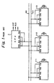
- Fig. 1 which illustrates a general communication system
- three communication apparatuses 1-1, 1-2 and 1-3 are connected to external buses X0 and X1 which are also connected to a CPU 2.
- Each of the communication apparatuses 1-1, 1-2 and 1-3 as well as the CPU 2 has receiving terminals RX0 and RX1 for receiving data from the external buses X0 and X1, and transmitting terminals TX0 and TX1 for transmitting data to the external buses X0 and X1.
- the CPU 2 generates various control signals such as a stop signal STP, a release signal RLS, and the like, and transmits them to the communication apparatuses 1-1, 1-2 and 1-3.
- the apparatus 1-i includes a comparator 11 for comparing the voltage RX0 at the external bus X0 with the voltage RX1 at the external bus X1, an oscillator 12 having a crystal resonator 12a, a voltage generator 13 for generating definite reference voltages VREF1 and VREF2, and a P-channel MOS transistor 14.
- the comparator 11 incorporates two differential amplifiers (current switches) for comparing the voltage RX0 with the voltage RX1. Each of the differential amplifiers receives the definite voltages VREF0 and VREF1, respectively, which will be explained with reference to Fig. 3.
- the oscillator 12 has a stop terminal STP and a release terminal RST.
- the clock signal CLK is supplied to various portions of the communication apparatus 1-i.
- the power of the comparator 11 is turned ON and OFF by the transistor 14 upon receipt of the stop signal STP from the CPU 2.
- the power of the oscillator 12 is turned OFF by receiving the stop signal STP, while the power of the oscillator 12 is turned ON by receiving the release signal RLS from the CPU 2. That is, in a stop mode where the stop signal STP is high ("1"), the comparator 11 and the oscillator 12 are inactive, while, in a non-stop mode where the stop signal is low (“0"), the comparator 11 is active, and also, the oscillator 12 is active upon receipt of the release signal RLS.
- the voltage generator 13 includes two P-channel MOS transistors 131 and 132 forming a current mirror circuit, and two drain-gate connected N-channel MOS transistors 133 and 134.
- the reference voltages VREF1 and VREF2 are definite.
- the comparator 11 includes a differential amplifier 111 for amplifying the difference between the voltages RX0 and RX1, a differential amplifier 112 for amplifying the difference between the voltage RX0 and RX1, and an output buffer 113, connected to the differential amplifiers 111 and 112, for generating an output signal RXD which is transmitted to an internal transmission/reception circuit (not shown).
- the differential amplifier 111 includes two P-channel MOS transistors 1111 and 1112 forming a current mirror circuit, two P-channel MOS transistors 1113 and 1114 forming a current mirror circuit, two N-channel MOS transistors 1115 and 1116 connected to the transistors 1112 and 1113, respectively, and an N-channel MOS transistor 1117 connected to the transistors 1115 and 1116.
- the transistor 1117 serves as a circuit source I 1 whose value is determined by the definite reference voltage VREF1.
- the differential amplifier 112 includes two N-channel MOS transistors 1121 and 1122 forming a current mirror circuit, two P-channel MOS transistors 1123 and 1124 connected to the transistors 1121 and 1122, respectively, and a P-channel MOS transistor 1125 connected to the transistors 1123 and 1124.
- the transistor 1125 serves as a circuit source I 2 whose value is determined by the definite reference voltage VREF2.
- the output buffer 113 includes two P-channel MOS transistors 1131 and 1132 forming a current mirror circuit, and two N-channel MOS transistors 1133 and 1134 for receiving the outputs of the differential amplifiers 111 and 112.
- the comparator 11 of Fig. 3 operates as follows.
- the differential amplifier 111 which serves as a current switch, the transistor 1115 is turned ON and the transistor 1116 is turned OFF.
- a current is supplied from the transistor 111 to the gate of the transistor 1134 of the output buffer 113, while very little current is supplied to the gate of the transistor 1133.
- the differential amplifier 112 which serves as a current switch, the transistor 1124 is turned ON and the transistor 1123 is turned OFF.
- a current is supplied from the transistor 1125 via the transistor 1124 to the gate of the transistor 1134 of the output buffer 113, while very little current is supplied to the gate of the transistor 1133.
- the comparator 11 of Fig. 3 operates as follows.
- the transistor 1116 is turned ON and the transistor 1115 is turned OFF.
- a current is supplied from the transistor 114 to the gate of the transistor 1133 of the output buffer 113, while very little current is supplied to the gate of the transistor 1134.
- the transistor 1123 is turned ON and the transistor 1124 is turned OFF.
- a current is supplied from the transistor 1125 via the transistor 1123 to the gate of the transistor 1133 of the output buffer 113, while very little current is supplied to the gate of the transistor 1134.
- At least one of the value of the current source I 1 and the value of the current source I 2 is increased.
- the conductivity of the transistor 133 of the voltage generator 13 is made large to thereby increase the current flowing through the transistor 132 as well as the current flowing through the transistor 131, the reference voltage VREF1 is increased so as to increase the value of the current source I 1 and the voltage VREF2 is decreased so as to increase the value of the current source I 2 .
- the operation speed of the differential amplifiers 111 and 112 is increased, i.e., the operation speed of the comparator 11 is increased.
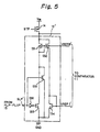
- a communication apparatus 1'-i includes a voltage generator 13' for generating variable reference voltages VREF1' and VREF2' instead of the voltage generator 13 of Fig. 2. That is, as illustrated in Fig. 5, the voltage generator 13' includes an N-channel MOS transistor 135 and an inverter 136 in addition to the elements of the voltage generator 13 of Fig. 3. In this case, the conductivity of the transistor 135 is less than that of the transistor 133. For example, the ratio W/L (W is a gate width; L is a gate length) of the transistor 135 is smaller than that of the transistor 133.
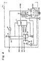
- a flip-flop 15, an OR circuit 16, a fall detector 17, an OR circuit 18, and a gate circuit 19 are added to the elements of Fig. 2.
- the flip-flop 15 is set by receiving a sleep signal SLP from the CPU 2 or the like.
- the OR circuit 16 passes an output signal of the flip-flop 15, i.e., the input signal SLP' of the voltage generator 13' to the stop terminal STP of the oscillator 12.
- the fall detector 17 detects a fall in the output signal RXD of the comparator 11, to thereby generate a signal RLS' having a definite time period.
- the fall detector 17 may be formed by a monostable multivibrator.
- the OR circuit 18 passes the signal RLS' as well as the release signal RLS to the release terminal RLS of the oscillator 12 and to the gate circuit 19.
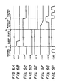
- the communication apparatus 1'-i enters a sleep state, i.e., a standby mode state. That is, as shown in Fig. 6C, the output SLP' of the flip-flop 15 is changed from "0" to "1", and as a result, as shown in Fig. 6H, the oscillator 12 enters a non-oscillating operation mode. Simultaneously, the reference voltages VREF1' and VREF2' of the voltage generator 13' satisfy the formulae (3) and (4), so that the comparator 11 enters in a low speed operation mode. Thus, the power dissipation of the communication apparatus 1'-i is reduced.
- the signal RLS' is supplied as a release signal to the release terminal RLS of the oscillator 12, so that, at time t 3 , the oscillator 12 enters an oscillating operation mode. Simultaneously, the gate circuit 19 generates a high level signal to reset the flip-flop 15. Thus, the voltages VREF1' and VREF2' of the voltage generator 13' satisfy the formulae (1) and (2), and accordingly, the comparator 11 returns to a high speed operation mode.
- a transition time period from time t 2 to time t 3 is defined as a wake-up state switched from the sleep state to the normal state.
- the delay time of the comparator 11 in a low speed operation mode is not so large, so that the wake-up time period is less than a one-bit transfer time period, thus avoiding incomplete reception of data.
- a rise detector 17' is provided instead of the fall detector 17 of Fig. 4. Therefore, when a rise occurs in the output of the comparator 11, the communication apparatus 1'-i of Fig. 7 is woke up from a sleep state to return to a normal state.
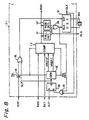
- a rise detector 17' added to the elements of Fig. 4. Therefore, when a fall or a rise occurs in the output of the comparator 11, the communication apparatus 1'-i of Fig. 8 is woke up from a sleep state to return to a normal state.
- a selector 20 is interposed between the outputs of the fall detector 17 and the rise detector 17' and the input of the OR circuit 18 in Fig. 8.
- the selector 20 is set in advance by a select signal S from the CPU 2 or the like. If the selector 20 selects the output of the fall detector 17, the communication apparatus of Fig. 9 operates in the same way as the communication apparatus of Fig. 4. Conversely, if the selector 20 selects the output of the rise detector 17', the communication apparatus of Fig. 9 operates in the same way as the communication apparatus of Fig. 7.
- the comparator 11 includes two-stage differential amplifiers (current switches); however, the present invention can be applied to a comparator having a single differential amplifier (current switch).
Landscapes
- Engineering & Computer Science (AREA)
- Signal Processing (AREA)
- Computer Networks & Wireless Communication (AREA)
- Quality & Reliability (AREA)
- Logic Circuits (AREA)
- Communication Control (AREA)
- Small-Scale Networks (AREA)
Claims (7)
- Kommunikationsvorrichtung, die mit einer Vielzahl von externen Bussen (X0, X1) verbunden ist, welche Vorrichtung Folgendes aufweist:einen Komparator (11), der mit den externen Bussen verbunden ist, zum Vergleichen der Spannung bei einem der externen Busse mit derjenigen bei einem anderen der externen Busse, um ein Ausgangssignal (RXD) zu erzeugen, wobei der Komparator einen Hochgeschwindigkeits-Betriebsmode und einen Niedergeschwindigkeits-Betriebsmode hat;einen Oszillator (12) mit einem oszillierenden Betriebsmode und einem nichtoszillierenden Betriebsmode;eine Ruheeinrichtung (15, 13'), die mit dem Komparator und dem Oszillator verbunden ist, zum Versetzen des Komparators in den Niedergeschwindigkeits-Betriebsmode und zum Versetzen des Oszillators in den nichtoszillierenden Mode;eine Erfassungseinrichtung (17, 17'), die mit einem Ausgang des Komparators verbunden ist, zum Erfassen wenigstens entweder eines Abfalls oder eines Anstiegs bezüglich der Spannung seines Ausgangssignals, um den Oszillator in den oszillierenden Betriebsmode zu versetzen; undeine Rücksetzeinrichtung (19), die mit der Erfassungseinrichtung, dem Oszillator und der Ruheeinrichtung verbunden ist, zum Rücksetzen der Ruheeinrichtung, wenn die Erfassungseinrichtung wenigstens entweder einen Abfall oder einen Anstieg bezüglich der Spannung des Ausgangssignals des Komparators erfasst und der Oszillator im oszillierenden Betriebsmode ist.
- Vorrichtung nach Anspruch 1, wobei der Komparator einen Stromschalter (1111∼1116, 1121∼1124) zum Empfangen der Spannungen bei den zwei externen Bussen aufweist, und eine mit dem Stromschalter verbundene Stromquelle (1117, 1125),
wobei die Stromquelle durch die Ruheeinrichtung so gesteuert wird, dass ein Strom, der durch die Stromquelle fließt, im Hochgeschwindigkeits-Betriebsmode größer als im Niedergeschwindigkeits-Betriebsmode ist. - Kommunikationsvorrichtung nach Anspruch 2, wobei die Ruheeinrichtung einen Spannungsgenerator (13') zum Erzeugen einer Spannung (VREF1', VREF2') enthält, deren Wert gemäß dem Betrieb der Ruheeinrichtung variiert wird, und zum Anlegen dieser Spannung an die Stromquelle, um dadurch die Stromquelle zu steuern.
- Kommunikationsvorrichtung nach Anspruch 1, wobei die Ruheeinrichtung folgendes aufweist:wobei der Komparator (11) den Hochgeschwindigkeits-Betriebsmode hat, wenn er die erste Spannung vom Spannungsgenerator empfängt, und den Niedergeschwindigkeits-Betriebsmode, wenn er die zweite Spannung vom Spannungsgenerator empfängt;ein Flip-Flop (15), das durch Empfangen eines Ruhesignals (SLP) gesetzt wird; undeinen Spannungsgenerator (13'), der mit einem Ausgang des Flip-Flops verbunden ist, zum Erzeugen einer ersten Spannung, wenn das Flip-Flop rückgesetzt ist, und zum Erzeugen einer zweiten Spannung, wenn das Flip-Flop gesetzt ist;
wobei der Oszillator in einem nichtoszillierenden Betriebsmode ist, wenn das Flip-Flop gesetzt ist;
wobei die Erfassungseinrichtung einen Abfalldetektor (17) zum Erfassen eines Abfalls bezüglich des Ausgangssignals aufweist, um ein Freigabesignal (RLS') zum Versetzen des Oszillators in den oszillierenden Betriebsmode zu erzeugen;
wobei die Rücksetzeinrichtung eine Gatterschaltung (19) zum Rücksetzen des Flip-Flops aufweist, wenn das Freigabesignal vom Abfalldetektor erzeugt wird und der Oszillator im oszillierenden Betriebsmode ist. - Kommunikationsvorrichtung nach Anspruch 1, wobei die Ruheeinrichtung Folgendes aufweist:wobei der Komparator den Hochgeschwindigkeits-Betriebsmode hat, wenn er die erste Spannung vom Spannungsgenerator empfängt, und den Niedergeschwindigkeits-Betriebsmode, wenn er die zweite Spannung vom Spannungsgenerator empfängt;ein Flip-Flop (15), das durch Empfangen eines Ruhesignals (SLP) gesetzt wird; undeinen Spannungsgenerator (13'), der mit einem Ausgang des Flip-Flops verbunden ist, zum Erzeugen einer ersten Spannung, wenn das Flip-Flop rückgesetzt ist, und zum Erzeugen einer zweiten Spannung, wenn das Flip-Flop gesetzt ist;
wobei der Oszillator im nichtoszillierenden Betriebsmode ist, wenn das Flip-Flop gesetzt ist;
wobei die Erfassungseinrichtung einen Anstiegsdetektor (17') zum Erfassen eines Anstiegs bezüglich des Ausgangssignals aufweist, um ein Freigabesignal (RLS') zum Versetzen des Oszillators in den oszillierenden Betriebsmode aufweist;
wobei die Rücksetzeinrichtung eine Gatterschaltung (19) zum Rücksetzen des Flip-Flop aufweist, wenn das Freigabesignal vom Anstiegsdetektor erzeugt wird und der Oszillator im oszillierenden Betriebsmode ist. - Kommunikationsvorrichtung nach Anspruch 1, wobei die Ruheeinrichtung Folgendes aufweist:wobei der Komparator den Hochgeschwindigkeits-Betriebsmode hat, wenn er die erste Spannung vom Spannungsgenerator empfängt, und den Niedergeschwindigkeits-Betriebsmode, wenn er die zweite Spannung vom Spannungsgenerator empfängt;ein Flip-Flop (15), das durch Empfangen eines Ruhesignals (SLP) gesetzt wird; undeinen Spannungsgenerator (13'), der mit einem Ausgang des Flip-Flops verbunden ist, zum Erzeugen einer ersten Spannung, wenn das Flip-Flop rückgesetzt ist, und zum Erzeugen einer zweiten Spannung, wenn das Flip-Flop gesetzt ist;
wobei der Oszillator im nichtoszillierenden Betriebsmode ist, wenn das Flip-Flop gesetzt ist;
wobei die Erfassungseinrichtung einen Abfalldetektor (17) zum Erfassen eines Abfalls bezüglich des Ausgangssignals aufweist, um ein Freigabesignal (RLS') zum Versetzen des Oszillators in den oszillierenden Betriebsmode zu erzeugen;
einen Anstiegsdetektor (17') zum Erfassen eines Anstiegs im Ausgangssignal, um ein Freigabesignal (RLS') zum Versetzen des Oszillators in den oszillierenden Betriebsmode zu erzeugen;
eine ODER-Schaltung (18), die mit dem Abfalldetektor und dem Anstiegsdetektor verbunden ist;
wobei die Rücksetzeinrichtung eine Gatterschaltung (19) aufweist, die mit der ODER-Schaltung verbunden ist, zum Rücksetzen des Flip-Flops, wenn das Freigabesignal von der ODER-Schaltung erzeugt wird und der Oszillator im oszillierenden Betriebsmode ist. - Kommunikationsvorrichtung nach Anspruch 1, wobei die Ruheeinrichtung folgendes aufweist:wobei der Komparator den Hochgeschwindigkeits-Betriebsmode hat, wenn er die erste Spannung vom Spannungsgenerator empfängt, und den Niedergeschwindigkeits-Betriebsmode, wenn er die zweite Spannung vom Spannungsgenerator empfängt;ein Flip-Flop (15), das durch Empfangen eines Ruhesignals (SLP) gesetzt wird; undeinen Spannungsgenerator (13'), der mit einem Ausgang des Flip-Flops verbunden ist, zum Erzeugen einer ersten Spannung, wenn das Flip-Flop rückgesetzt ist, und zum Erzeugen einer zweiten Spannung, wenn das Flip-Flop gesetzt ist;
wobei der Oszillator im nichtoszillierenden Betriebsmode ist, wenn das Flip-Flop gesetzt ist;
wobei die Erfassungseinrichtung folgendes aufweist:wobei die Rücksetzeinrichtung eine Gatterschaltung (19) aufweist, die mit dem Selektor verbunden ist, zum Rücksetzen des Flip-Flops, wenn das Freigabesignal vom Selektor erzeugt wird und der Oszillator im oszillierenden Betriebsmode ist.einen Abfalldetektor (17) zum Erfassen eines Abfalls bezüglich des Ausgangssignals, um ein Freigabesignal (RLS') zum Versetzen des Oszillators in den oszillierenden Betriebsmode zu erzeugen;einen Anstiegsdetektor (17') zum Erfassen eines Anstiegs bezüglich des Ausgangssignals, um ein Freigabesignal (RLS') zum Versetzen des Oszillators in einen oszillierenden Betriebsmode zu erzeugen; undeinen Selektor (20), der mit dem Abfalldetektor und dem Anstiegsdetektor verbunden ist, zum Auswählen entweder des Abfalldetektors oder des Anstiegsdetektors;
Applications Claiming Priority (3)
| Application Number | Priority Date | Filing Date | Title |
|---|---|---|---|
| JP4326356A JP2870337B2 (ja) | 1992-12-07 | 1992-12-07 | 通信装置 |
| JP326356/92 | 1992-12-07 | ||
| JP32635692 | 1992-12-07 |
Publications (3)
| Publication Number | Publication Date |
|---|---|
| EP0601539A2 EP0601539A2 (de) | 1994-06-15 |
| EP0601539A3 EP0601539A3 (en) | 1995-09-06 |
| EP0601539B1 true EP0601539B1 (de) | 2002-05-02 |
Family
ID=18186883
Family Applications (1)
| Application Number | Title | Priority Date | Filing Date |
|---|---|---|---|
| EP93119694A Expired - Lifetime EP0601539B1 (de) | 1992-12-07 | 1993-12-07 | Übertragungsvorrichtung mit geringer Leistungsaufnahme |
Country Status (5)
| Country | Link |
|---|---|
| US (1) | US5440595A (de) |
| EP (1) | EP0601539B1 (de) |
| JP (1) | JP2870337B2 (de) |
| KR (1) | KR960014981B1 (de) |
| DE (1) | DE69331872T2 (de) |
Families Citing this family (5)
| Publication number | Priority date | Publication date | Assignee | Title |
|---|---|---|---|---|
| US6111911A (en) * | 1995-06-07 | 2000-08-29 | Sanconix, Inc | Direct sequence frequency ambiguity resolving receiver |
| DE19831942A1 (de) | 1998-07-16 | 2000-01-20 | Alcatel Sa | Empfänger eines Telekommunikationsnetzes |
| US6810216B1 (en) * | 1999-07-02 | 2004-10-26 | Nokia Corporation | Fast infrared transceiver with reduced power consumption |
| US8358175B2 (en) * | 2011-05-10 | 2013-01-22 | Nxp B.V. | Oscillator architecture having fast response time with low current consumption and method for operating the oscillator architecture |
| CN112685348B (zh) * | 2021-01-11 | 2023-08-08 | 云淡风轻(广州)智能科技有限公司 | 一种适用于低速单片机的高速单线通信系统及方法 |
Family Cites Families (4)
| Publication number | Priority date | Publication date | Assignee | Title |
|---|---|---|---|---|
| JPS60170344A (ja) * | 1984-02-14 | 1985-09-03 | Matsushita Electric Ind Co Ltd | 選択呼出受信装置 |
| US4803702A (en) * | 1986-08-05 | 1989-02-07 | Advanced Micro Devices, Inc. | Reset and synchronization interface circuit |
| US4893094A (en) * | 1989-03-13 | 1990-01-09 | Motorola, Inc. | Frequency synthesizer with control of start-up battery saving operations |
| US5155453A (en) * | 1991-05-23 | 1992-10-13 | Samsung Semiconductor, Inc. | Low-power crystal oscillator |
-
1992
- 1992-12-07 JP JP4326356A patent/JP2870337B2/ja not_active Expired - Fee Related
-
1993
- 1993-12-07 US US08/162,274 patent/US5440595A/en not_active Expired - Fee Related
- 1993-12-07 EP EP93119694A patent/EP0601539B1/de not_active Expired - Lifetime
- 1993-12-07 DE DE69331872T patent/DE69331872T2/de not_active Expired - Fee Related
- 1993-12-07 KR KR1019930026680A patent/KR960014981B1/ko not_active Expired - Fee Related
Also Published As
| Publication number | Publication date |
|---|---|
| EP0601539A2 (de) | 1994-06-15 |
| KR940015751A (ko) | 1994-07-21 |
| US5440595A (en) | 1995-08-08 |
| JPH06177932A (ja) | 1994-06-24 |
| DE69331872D1 (de) | 2002-06-06 |
| KR960014981B1 (ko) | 1996-10-23 |
| JP2870337B2 (ja) | 1999-03-17 |
| DE69331872T2 (de) | 2002-11-28 |
| EP0601539A3 (en) | 1995-09-06 |
Similar Documents
| Publication | Publication Date | Title |
|---|---|---|
| JP4168326B2 (ja) | 差動カスコードスイッチを使用するパルスdフリップフロップ | |
| US6363031B2 (en) | Circuit, architecture and method for reducing power consumption in a synchronous integrated circuit | |
| US6097243A (en) | Device and method to reduce power consumption in integrated semiconductor devices using a low power groggy mode | |
| US5793227A (en) | Synchronizing logic avoiding metastability | |
| JPH0329510A (ja) | 半導体集積回路内の電圧変換回路 | |
| US5629643A (en) | Feedback latch and method therefor | |
| US7639745B2 (en) | Serial data link with automatic power down | |
| US6621306B2 (en) | Random logic circuit | |
| US6373309B1 (en) | Duty cycle compensation circuit of delay locked loop for Rambus DRAM | |
| KR20000009772A (ko) | 메모리용 저전력 감지 증폭기 | |
| US5440248A (en) | Power-saver differential input buffer | |
| US5440595A (en) | Communication apparatus with low power consumption | |
| KR100348221B1 (ko) | 고전압 발생기 | |
| US5903508A (en) | Input buffer of memory device for reducing current consumption in standby mode | |
| US5610544A (en) | Semiconductor integrated circuit free from through current due to source-voltage drop | |
| JPH11317648A (ja) | リングオシレータ | |
| US6140714A (en) | Power control apparatus for a battery-powered communication system | |
| US5994931A (en) | Method and circuit configuration for controlling operating states of a second device by means of a first device | |
| US6359489B1 (en) | Clock signal generation and buffer circuit having high noise immunity and low power consumption | |
| US6130558A (en) | Data transfer circuit and method for a semiconductor memory | |
| US6160422A (en) | Power saving clock buffer | |
| US20020140485A1 (en) | Low current clock sensor | |
| US6297682B1 (en) | Differential sense amplifier circuit | |
| US6462613B1 (en) | Power controlled input receiver | |
| US7573755B2 (en) | Data amplifying circuit for semiconductor integrated circuit |
Legal Events
| Date | Code | Title | Description |
|---|---|---|---|
| PUAI | Public reference made under article 153(3) epc to a published international application that has entered the european phase |
Free format text: ORIGINAL CODE: 0009012 |
|
| AK | Designated contracting states |
Kind code of ref document: A2 Designated state(s): DE FR GB IT NL |
|
| PUAL | Search report despatched |
Free format text: ORIGINAL CODE: 0009013 |
|
| AK | Designated contracting states |
Kind code of ref document: A3 Designated state(s): DE FR GB IT NL |
|
| 17P | Request for examination filed |
Effective date: 19951220 |
|
| 17Q | First examination report despatched |
Effective date: 20000324 |
|
| GRAG | Despatch of communication of intention to grant |
Free format text: ORIGINAL CODE: EPIDOS AGRA |
|
| GRAG | Despatch of communication of intention to grant |
Free format text: ORIGINAL CODE: EPIDOS AGRA |
|
| GRAH | Despatch of communication of intention to grant a patent |
Free format text: ORIGINAL CODE: EPIDOS IGRA |
|
| REG | Reference to a national code |
Ref country code: GB Ref legal event code: IF02 |
|
| GRAH | Despatch of communication of intention to grant a patent |
Free format text: ORIGINAL CODE: EPIDOS IGRA |
|
| GRAA | (expected) grant |
Free format text: ORIGINAL CODE: 0009210 |
|
| AK | Designated contracting states |
Kind code of ref document: B1 Designated state(s): DE FR GB IT NL |
|
| REG | Reference to a national code |
Ref country code: GB Ref legal event code: FG4D |
|
| REF | Corresponds to: |
Ref document number: 69331872 Country of ref document: DE Date of ref document: 20020606 |
|
| ET | Fr: translation filed | ||
| PLBE | No opposition filed within time limit |
Free format text: ORIGINAL CODE: 0009261 |
|
| STAA | Information on the status of an ep patent application or granted ep patent |
Free format text: STATUS: NO OPPOSITION FILED WITHIN TIME LIMIT |
|
| REG | Reference to a national code |
Ref country code: GB Ref legal event code: 732E |
|
| 26N | No opposition filed |
Effective date: 20030204 |
|
| NLS | Nl: assignments of ep-patents |
Owner name: NEC ELECTRONICS CORPORATION |
|
| REG | Reference to a national code |
Ref country code: FR Ref legal event code: TP |
|
| PGFP | Annual fee paid to national office [announced via postgrant information from national office to epo] |
Ref country code: GB Payment date: 20031203 Year of fee payment: 11 |
|
| PGFP | Annual fee paid to national office [announced via postgrant information from national office to epo] |
Ref country code: NL Payment date: 20031205 Year of fee payment: 11 |
|
| PGFP | Annual fee paid to national office [announced via postgrant information from national office to epo] |
Ref country code: FR Payment date: 20031210 Year of fee payment: 11 |
|
| PGFP | Annual fee paid to national office [announced via postgrant information from national office to epo] |
Ref country code: DE Payment date: 20031218 Year of fee payment: 11 |
|
| PG25 | Lapsed in a contracting state [announced via postgrant information from national office to epo] |
Ref country code: GB Free format text: LAPSE BECAUSE OF NON-PAYMENT OF DUE FEES Effective date: 20041207 |
|
| PG25 | Lapsed in a contracting state [announced via postgrant information from national office to epo] |
Ref country code: NL Free format text: LAPSE BECAUSE OF NON-PAYMENT OF DUE FEES Effective date: 20050701 Ref country code: DE Free format text: LAPSE BECAUSE OF NON-PAYMENT OF DUE FEES Effective date: 20050701 |
|
| GBPC | Gb: european patent ceased through non-payment of renewal fee |
Effective date: 20041207 |
|
| PG25 | Lapsed in a contracting state [announced via postgrant information from national office to epo] |
Ref country code: FR Free format text: LAPSE BECAUSE OF NON-PAYMENT OF DUE FEES Effective date: 20050831 |
|
| NLV4 | Nl: lapsed or anulled due to non-payment of the annual fee |
Effective date: 20050701 |
|
| REG | Reference to a national code |
Ref country code: FR Ref legal event code: ST |
|
| PG25 | Lapsed in a contracting state [announced via postgrant information from national office to epo] |
Ref country code: IT Free format text: LAPSE BECAUSE OF NON-PAYMENT OF DUE FEES;WARNING: LAPSES OF ITALIAN PATENTS WITH EFFECTIVE DATE BEFORE 2007 MAY HAVE OCCURRED AT ANY TIME BEFORE 2007. THE CORRECT EFFECTIVE DATE MAY BE DIFFERENT FROM THE ONE RECORDED. Effective date: 20051207 |