EP0602421A2 - Réseaux logiques programmables à haute performance et à faible consommation - Google Patents
Réseaux logiques programmables à haute performance et à faible consommation Download PDFInfo
- Publication number
- EP0602421A2 EP0602421A2 EP93118892A EP93118892A EP0602421A2 EP 0602421 A2 EP0602421 A2 EP 0602421A2 EP 93118892 A EP93118892 A EP 93118892A EP 93118892 A EP93118892 A EP 93118892A EP 0602421 A2 EP0602421 A2 EP 0602421A2
- Authority
- EP
- European Patent Office
- Prior art keywords
- lines
- input
- array
- product term
- decoder
- Prior art date
- Legal status (The legal status is an assumption and is not a legal conclusion. Google has not performed a legal analysis and makes no representation as to the accuracy of the status listed.)
- Granted
Links
Images


Classifications
-
- H—ELECTRICITY
- H03—ELECTRONIC CIRCUITRY
- H03K—PULSE TECHNIQUE
- H03K19/00—Logic circuits, i.e. having at least two inputs acting on one output; Inverting circuits
- H03K19/0008—Arrangements for reducing power consumption
- H03K19/0016—Arrangements for reducing power consumption by using a control or a clock signal, e.g. in order to apply power supply
-
- H—ELECTRICITY
- H03—ELECTRONIC CIRCUITRY
- H03K—PULSE TECHNIQUE
- H03K19/00—Logic circuits, i.e. having at least two inputs acting on one output; Inverting circuits
- H03K19/02—Logic circuits, i.e. having at least two inputs acting on one output; Inverting circuits using specified components
- H03K19/173—Logic circuits, i.e. having at least two inputs acting on one output; Inverting circuits using specified components using elementary logic circuits as components
- H03K19/177—Logic circuits, i.e. having at least two inputs acting on one output; Inverting circuits using specified components using elementary logic circuits as components arranged in matrix form
- H03K19/17704—Logic circuits, i.e. having at least two inputs acting on one output; Inverting circuits using specified components using elementary logic circuits as components arranged in matrix form the logic functions being realised by the interconnection of rows and columns
- H03K19/17708—Logic circuits, i.e. having at least two inputs acting on one output; Inverting circuits using specified components using elementary logic circuits as components arranged in matrix form the logic functions being realised by the interconnection of rows and columns using an AND matrix followed by an OR matrix, i.e. programmable logic arrays
- H03K19/17716—Logic circuits, i.e. having at least two inputs acting on one output; Inverting circuits using specified components using elementary logic circuits as components arranged in matrix form the logic functions being realised by the interconnection of rows and columns using an AND matrix followed by an OR matrix, i.e. programmable logic arrays with synchronous operation, i.e. using clock signals, e.g. of I/O or coupling register
- H03K19/1772—Logic circuits, i.e. having at least two inputs acting on one output; Inverting circuits using specified components using elementary logic circuits as components arranged in matrix form the logic functions being realised by the interconnection of rows and columns using an AND matrix followed by an OR matrix, i.e. programmable logic arrays with synchronous operation, i.e. using clock signals, e.g. of I/O or coupling register with synchronous operation of at least one of the logical matrixes
Definitions
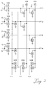
- U.S. Pat. No. 4,697,105 entitled "CMOS Programmable Logic Array,” which issued on Sep. 29, 1987 and was assigned to the American Telephone and Telephone Company, AT&T Bell Laboratories, discloses a PLA including a dynamic AND plane and an OR plane using clock load devices.
- the high precharged voltage state in the AND plane places the logic lines in the OR plane in a low voltage state during precharge.
- the OR logic lines may then be pulled to a high level during the decode operation.
- a clock having a delay path is used to control the precharge and decode operations of the PLA.
- a significant disadvantage of the array shown in the Fig. 1 is the fact that the pullup devices are always in the on state, resulting in a significant power consumption.
- Pre-decode ⁇ x2, x3 ⁇
Landscapes
- Physics & Mathematics (AREA)
- Mathematical Physics (AREA)
- Engineering & Computer Science (AREA)
- Computer Hardware Design (AREA)
- Computing Systems (AREA)
- General Engineering & Computer Science (AREA)
- Logic Circuits (AREA)
Applications Claiming Priority (2)
| Application Number | Priority Date | Filing Date | Title |
|---|---|---|---|
| US992216 | 1992-12-17 | ||
| US07/992,216 US5311079A (en) | 1992-12-17 | 1992-12-17 | Low power, high performance PLA |
Publications (3)
| Publication Number | Publication Date |
|---|---|
| EP0602421A2 true EP0602421A2 (fr) | 1994-06-22 |
| EP0602421A3 EP0602421A3 (fr) | 1995-03-29 |
| EP0602421B1 EP0602421B1 (fr) | 1997-07-02 |
Family
ID=25538054
Family Applications (1)
| Application Number | Title | Priority Date | Filing Date |
|---|---|---|---|
| EP93118892A Expired - Lifetime EP0602421B1 (fr) | 1992-12-17 | 1993-11-24 | Réseaux logiques programmables à haute performance et à faible consommation |
Country Status (4)
| Country | Link |
|---|---|
| US (1) | US5311079A (fr) |
| EP (1) | EP0602421B1 (fr) |
| JP (1) | JP2625638B2 (fr) |
| DE (1) | DE69311882D1 (fr) |
Families Citing this family (33)
| Publication number | Priority date | Publication date | Assignee | Title |
|---|---|---|---|---|
| US5452215A (en) * | 1994-08-24 | 1995-09-19 | Ibm Business Machines Corporation | System and method for designing a finite state machine to reduce power dissipation |
| US5719505A (en) * | 1995-04-11 | 1998-02-17 | International Business Machines Corporation | Reduced power PLA |
| US5712790A (en) * | 1995-04-11 | 1998-01-27 | International Business Machines Corporation | Method of power reduction in pla's |
| US7266725B2 (en) | 2001-09-03 | 2007-09-04 | Pact Xpp Technologies Ag | Method for debugging reconfigurable architectures |
| DE19651075A1 (de) | 1996-12-09 | 1998-06-10 | Pact Inf Tech Gmbh | Einheit zur Verarbeitung von numerischen und logischen Operationen, zum Einsatz in Prozessoren (CPU's), Mehrrechnersystemen, Datenflußprozessoren (DFP's), digitalen Signal Prozessoren (DSP's) oder dergleichen |
| DE19654595A1 (de) | 1996-12-20 | 1998-07-02 | Pact Inf Tech Gmbh | I0- und Speicherbussystem für DFPs sowie Bausteinen mit zwei- oder mehrdimensionaler programmierbaren Zellstrukturen |
| US5867038A (en) * | 1996-12-20 | 1999-02-02 | International Business Machines Corporation | Self-timed low power ratio-logic system having an input sensing circuit |
| ATE243390T1 (de) | 1996-12-27 | 2003-07-15 | Pact Inf Tech Gmbh | Verfahren zum selbständigen dynamischen umladen von datenflussprozessoren (dfps) sowie bausteinen mit zwei- oder mehrdimensionalen programmierbaren zellstrukturen (fpgas, dpgas, o.dgl.) |
| US6542998B1 (en) | 1997-02-08 | 2003-04-01 | Pact Gmbh | Method of self-synchronization of configurable elements of a programmable module |
| US8686549B2 (en) | 2001-09-03 | 2014-04-01 | Martin Vorbach | Reconfigurable elements |
| DE19861088A1 (de) | 1997-12-22 | 2000-02-10 | Pact Inf Tech Gmbh | Verfahren zur Reparatur von integrierten Schaltkreisen |
| CN1378665A (zh) | 1999-06-10 | 2002-11-06 | Pact信息技术有限公司 | 编程概念 |
| JP2004506261A (ja) | 2000-06-13 | 2004-02-26 | ペーアーツェーテー イクスペーペー テクノロジーズ アクチエンゲゼルシャフト | パイプラインctプロトコルおよびct通信 |
| US7065732B1 (en) * | 2000-09-28 | 2006-06-20 | Intel Corporation | Method to reduce the power consumption of large PLAs by clock gating guided by recursive shannon decomposition of the and-plane |
| JP2004517386A (ja) * | 2000-10-06 | 2004-06-10 | ペーアーツェーテー イクスペーペー テクノロジーズ アクチエンゲゼルシャフト | 方法および装置 |
| US8058899B2 (en) | 2000-10-06 | 2011-11-15 | Martin Vorbach | Logic cell array and bus system |
| US7444531B2 (en) | 2001-03-05 | 2008-10-28 | Pact Xpp Technologies Ag | Methods and devices for treating and processing data |
| US9037807B2 (en) | 2001-03-05 | 2015-05-19 | Pact Xpp Technologies Ag | Processor arrangement on a chip including data processing, memory, and interface elements |
| US7844796B2 (en) | 2001-03-05 | 2010-11-30 | Martin Vorbach | Data processing device and method |
| EP2224330B1 (fr) | 2001-06-20 | 2012-05-09 | Krass, Maren | Procede et systeme pour decouper des logiciels volumineux |
| US7996827B2 (en) | 2001-08-16 | 2011-08-09 | Martin Vorbach | Method for the translation of programs for reconfigurable architectures |
| US7434191B2 (en) | 2001-09-03 | 2008-10-07 | Pact Xpp Technologies Ag | Router |
| US8686475B2 (en) | 2001-09-19 | 2014-04-01 | Pact Xpp Technologies Ag | Reconfigurable elements |
| US7577822B2 (en) | 2001-12-14 | 2009-08-18 | Pact Xpp Technologies Ag | Parallel task operation in processor and reconfigurable coprocessor configured based on information in link list including termination information for synchronization |
| AU2003208266A1 (en) | 2002-01-19 | 2003-07-30 | Pact Xpp Technologies Ag | Reconfigurable processor |
| US8127061B2 (en) | 2002-02-18 | 2012-02-28 | Martin Vorbach | Bus systems and reconfiguration methods |
| US8914590B2 (en) | 2002-08-07 | 2014-12-16 | Pact Xpp Technologies Ag | Data processing method and device |
| AU2003286131A1 (en) | 2002-08-07 | 2004-03-19 | Pact Xpp Technologies Ag | Method and device for processing data |
| US7657861B2 (en) | 2002-08-07 | 2010-02-02 | Pact Xpp Technologies Ag | Method and device for processing data |
| US7394284B2 (en) | 2002-09-06 | 2008-07-01 | Pact Xpp Technologies Ag | Reconfigurable sequencer structure |
| JP4700611B2 (ja) | 2003-08-28 | 2011-06-15 | ペーアーツェーテー イクスペーペー テクノロジーズ アクチエンゲゼルシャフト | データ処理装置およびデータ処理方法 |
| US8250503B2 (en) | 2006-01-18 | 2012-08-21 | Martin Vorbach | Hardware definition method including determining whether to implement a function as hardware or software |
| US7693257B2 (en) * | 2006-06-29 | 2010-04-06 | Accuray Incorporated | Treatment delivery optimization |
Family Cites Families (10)
| Publication number | Priority date | Publication date | Assignee | Title |
|---|---|---|---|---|
| US4233667A (en) * | 1978-10-23 | 1980-11-11 | International Business Machines Corporation | Demand powered programmable logic array |
| JPS58170123A (ja) * | 1982-03-30 | 1983-10-06 | Fujitsu Ltd | プログラマブルロジツクアレイ |
| US4957601A (en) * | 1984-09-04 | 1990-09-18 | Texas Instruments Incorporated | Method of forming an array of apertures in an aluminum foil |
| US4831285A (en) * | 1988-01-19 | 1989-05-16 | National Semiconductor Corporation | Self precharging static programmable logic array |
| JP2547436B2 (ja) * | 1988-04-11 | 1996-10-23 | 富士通株式会社 | Pla制御方式 |
| US4963769A (en) * | 1989-05-08 | 1990-10-16 | Cypress Semiconductor | Circuit for selective power-down of unused circuitry |
| NL8902820A (nl) * | 1989-11-15 | 1991-06-03 | Philips Nv | Geintegreerde halfgeleiderschakeling van het master slice type. |
| US5111079A (en) * | 1990-06-29 | 1992-05-05 | Sgs-Thomson Microelectronics, Inc. | Power reduction circuit for programmable logic device |
| US5250859A (en) * | 1991-09-27 | 1993-10-05 | Kaplinsky Cecil H | Low power multifunction logic array |
| JPH05276019A (ja) * | 1992-03-30 | 1993-10-22 | Nec Corp | プログラマブル・ロジックアレイ回路 |
-
1992
- 1992-12-17 US US07/992,216 patent/US5311079A/en not_active Expired - Fee Related
-
1993
- 1993-11-24 EP EP93118892A patent/EP0602421B1/fr not_active Expired - Lifetime
- 1993-11-24 DE DE69311882T patent/DE69311882D1/de not_active Expired - Lifetime
- 1993-12-16 JP JP5316116A patent/JP2625638B2/ja not_active Expired - Lifetime
Also Published As
| Publication number | Publication date |
|---|---|
| EP0602421A3 (fr) | 1995-03-29 |
| JP2625638B2 (ja) | 1997-07-02 |
| EP0602421B1 (fr) | 1997-07-02 |
| JPH06232734A (ja) | 1994-08-19 |
| DE69311882D1 (de) | 1997-08-07 |
| US5311079A (en) | 1994-05-10 |
Similar Documents
| Publication | Publication Date | Title |
|---|---|---|
| EP0602421B1 (fr) | Réseaux logiques programmables à haute performance et à faible consommation | |
| JP3005644B2 (ja) | プログラマブル論理装置用入力回路及びプログラマブル論理装置で使用するための論理回路並びにプログラマブル論理装置 | |
| EP0601094B1 (fr) | Reseau et cellule logique programmable | |
| US6014038A (en) | Function block architecture for gate array | |
| US6556500B2 (en) | Programmable logic array device with random access memory configurable as product terms | |
| US5744981A (en) | Programmable logic cell with input polarity control | |
| US4506341A (en) | Interlaced programmable logic array having shared elements | |
| US5302866A (en) | Input circuit block and method for PLDs with register clock enable selection | |
| EP0613249A1 (fr) | Table de consultation personnalisée avec un nombre réduit des bits d'architecture | |
| EP0223308A2 (fr) | Dispositif logique programmable avec retour programmable afin de déterminer le nombre de niveaux logiques | |
| US6066965A (en) | Method and apparatus for a N-nary logic circuit using 1 of 4 signals | |
| JPH08330943A (ja) | 組合せ回路または順序回路として構成されうるフィールドプログラマブル・ゲートアレイ論理モジュール | |
| JPH0645912A (ja) | 構成を変更可能な記憶回路 | |
| US4675556A (en) | Binomially-encoded finite state machine | |
| US5614844A (en) | High speed programmable logic architecture | |
| US5497107A (en) | Multiple, selectable PLAS having shared inputs and outputs | |
| US6069497A (en) | Method and apparatus for a N-nary logic circuit using 1 of N signals | |
| US6097221A (en) | Semiconductor integrated circuit capable of realizing logic functions | |
| CA1204171A (fr) | Reseau logique programmable | |
| US5075576A (en) | Field-programmable logic device with programmable foldback to control number of logic levels | |
| US4525641A (en) | Flip-flop programmer using cascaded logic arrays | |
| JPH02222217A (ja) | プログラマブル論理回路 | |
| US5751162A (en) | Field programmable gate array logic module configurable as combinational or sequential circuits | |
| US5231389A (en) | Display control for selecting oscillating signals | |
| US4771284A (en) | Logic array with programmable element output generation |
Legal Events
| Date | Code | Title | Description |
|---|---|---|---|
| PUAI | Public reference made under article 153(3) epc to a published international application that has entered the european phase |
Free format text: ORIGINAL CODE: 0009012 |
|
| AK | Designated contracting states |
Kind code of ref document: A2 Designated state(s): DE FR GB |
|
| 17P | Request for examination filed |
Effective date: 19941021 |
|
| PUAL | Search report despatched |
Free format text: ORIGINAL CODE: 0009013 |
|
| AK | Designated contracting states |
Kind code of ref document: A3 Designated state(s): DE FR GB |
|
| GRAG | Despatch of communication of intention to grant |
Free format text: ORIGINAL CODE: EPIDOS AGRA |
|
| 17Q | First examination report despatched |
Effective date: 19960805 |
|
| GRAH | Despatch of communication of intention to grant a patent |
Free format text: ORIGINAL CODE: EPIDOS IGRA |
|
| GRAH | Despatch of communication of intention to grant a patent |
Free format text: ORIGINAL CODE: EPIDOS IGRA |
|
| GRAA | (expected) grant |
Free format text: ORIGINAL CODE: 0009210 |
|
| AK | Designated contracting states |
Kind code of ref document: B1 Designated state(s): DE FR GB |
|
| PG25 | Lapsed in a contracting state [announced via postgrant information from national office to epo] |
Ref country code: FR Effective date: 19970702 |
|
| REF | Corresponds to: |
Ref document number: 69311882 Country of ref document: DE Date of ref document: 19970807 |
|
| PG25 | Lapsed in a contracting state [announced via postgrant information from national office to epo] |
Ref country code: DE Effective date: 19971003 |
|
| PG25 | Lapsed in a contracting state [announced via postgrant information from national office to epo] |
Ref country code: GB Free format text: LAPSE BECAUSE OF NON-PAYMENT OF DUE FEES Effective date: 19971124 |
|
| EN | Fr: translation not filed | ||
| PLBE | No opposition filed within time limit |
Free format text: ORIGINAL CODE: 0009261 |
|
| STAA | Information on the status of an ep patent application or granted ep patent |
Free format text: STATUS: NO OPPOSITION FILED WITHIN TIME LIMIT |
|
| 26N | No opposition filed | ||
| GBPC | Gb: european patent ceased through non-payment of renewal fee |
Effective date: 19971124 |