EP0602466A2 - Régulateur de tension integré monolithique - Google Patents
Régulateur de tension integré monolithique Download PDFInfo
- Publication number
- EP0602466A2 EP0602466A2 EP93119431A EP93119431A EP0602466A2 EP 0602466 A2 EP0602466 A2 EP 0602466A2 EP 93119431 A EP93119431 A EP 93119431A EP 93119431 A EP93119431 A EP 93119431A EP 0602466 A2 EP0602466 A2 EP 0602466A2
- Authority
- EP
- European Patent Office
- Prior art keywords
- voltage
- voltage regulator
- current
- control loop
- starting
- Prior art date
- Legal status (The legal status is an assumption and is not a legal conclusion. Google has not performed a legal analysis and makes no representation as to the accuracy of the status listed.)
- Granted
Links
- 230000001105 regulatory effect Effects 0.000 claims abstract description 22
- 238000005516 engineering process Methods 0.000 claims description 7
- 239000000758 substrate Substances 0.000 claims description 7
- 238000012545 processing Methods 0.000 claims description 6
- 238000013461 design Methods 0.000 claims description 5
- 239000004065 semiconductor Substances 0.000 claims description 5
- 238000004519 manufacturing process Methods 0.000 claims description 3
- 230000004913 activation Effects 0.000 claims description 2
- 238000012546 transfer Methods 0.000 claims description 2
- 230000001788 irregular Effects 0.000 claims 1
- 238000010586 diagram Methods 0.000 description 8
- 230000001419 dependent effect Effects 0.000 description 7
- 230000003321 amplification Effects 0.000 description 2
- 230000008901 benefit Effects 0.000 description 2
- 239000003990 capacitor Substances 0.000 description 2
- 230000000295 complement effect Effects 0.000 description 2
- 230000000694 effects Effects 0.000 description 2
- 238000003199 nucleic acid amplification method Methods 0.000 description 2
- 230000004044 response Effects 0.000 description 2
- 230000005540 biological transmission Effects 0.000 description 1
- 238000006243 chemical reaction Methods 0.000 description 1
- 238000013016 damping Methods 0.000 description 1
- 238000011161 development Methods 0.000 description 1
- 230000018109 developmental process Effects 0.000 description 1
- 238000005259 measurement Methods 0.000 description 1
- 238000012544 monitoring process Methods 0.000 description 1
- 229920006395 saturated elastomer Polymers 0.000 description 1
- 238000007873 sieving Methods 0.000 description 1
- 230000006641 stabilisation Effects 0.000 description 1
- 238000011105 stabilization Methods 0.000 description 1
- 239000007858 starting material Substances 0.000 description 1
- 230000001629 suppression Effects 0.000 description 1
- 230000007704 transition Effects 0.000 description 1
Images


Classifications
-
- G—PHYSICS
- G05—CONTROLLING; REGULATING
- G05F—SYSTEMS FOR REGULATING ELECTRIC OR MAGNETIC VARIABLES
- G05F1/00—Automatic systems in which deviations of an electric quantity from one or more predetermined values are detected at the output of the system and fed back to a device within the system to restore the detected quantity to its predetermined value or values, i.e. retroactive systems
- G05F1/10—Regulating voltage or current
- G05F1/46—Regulating voltage or current wherein the variable actually regulated by the final control device is DC
- G05F1/56—Regulating voltage or current wherein the variable actually regulated by the final control device is DC using semiconductor devices in series with the load as final control devices
- G05F1/563—Regulating voltage or current wherein the variable actually regulated by the final control device is DC using semiconductor devices in series with the load as final control devices including two stages of regulation at least one of which is output level responsive, e.g. coarse and fine regulation
-
- G—PHYSICS
- G05—CONTROLLING; REGULATING
- G05F—SYSTEMS FOR REGULATING ELECTRIC OR MAGNETIC VARIABLES
- G05F1/00—Automatic systems in which deviations of an electric quantity from one or more predetermined values are detected at the output of the system and fed back to a device within the system to restore the detected quantity to its predetermined value or values, i.e. retroactive systems
- G05F1/10—Regulating voltage or current
- G05F1/46—Regulating voltage or current wherein the variable actually regulated by the final control device is DC
- G05F1/56—Regulating voltage or current wherein the variable actually regulated by the final control device is DC using semiconductor devices in series with the load as final control devices
- G05F1/575—Regulating voltage or current wherein the variable actually regulated by the final control device is DC using semiconductor devices in series with the load as final control devices characterised by the feedback circuit
-
- H—ELECTRICITY
- H03—ELECTRONIC CIRCUITRY
- H03F—AMPLIFIERS
- H03F1/00—Details of amplifiers with only discharge tubes, only semiconductor devices or only unspecified devices as amplifying elements
- H03F1/30—Modifications of amplifiers to reduce influence of variations of temperature or supply voltage or other physical parameters
- H03F1/305—Modifications of amplifiers to reduce influence of variations of temperature or supply voltage or other physical parameters in case of switching on or off of a power supply
-
- Y—GENERAL TAGGING OF NEW TECHNOLOGICAL DEVELOPMENTS; GENERAL TAGGING OF CROSS-SECTIONAL TECHNOLOGIES SPANNING OVER SEVERAL SECTIONS OF THE IPC; TECHNICAL SUBJECTS COVERED BY FORMER USPC CROSS-REFERENCE ART COLLECTIONS [XRACs] AND DIGESTS
- Y10—TECHNICAL SUBJECTS COVERED BY FORMER USPC
- Y10S—TECHNICAL SUBJECTS COVERED BY FORMER USPC CROSS-REFERENCE ART COLLECTIONS [XRACs] AND DIGESTS
- Y10S323/00—Electricity: power supply or regulation systems
- Y10S323/901—Starting circuits
Definitions
- the invention relates to a voltage regulator containing a control loop for generating a regulated supply voltage.
- the voltage regulator works as a series regulator, the actuator of which lies between a first and a second connection terminal, to which an unregulated supply voltage is connected or the regulated supply voltage can be tapped.
- a third connection terminal connects the voltage regulator to a fixed reference potential, which is usually the ground potential.
- the control loop contains a reference network which supplies the signals for the target / actual comparison, a differential device with a first amplification factor, which generates a signal which is dependent on the control deviation, and the actuator with a second amplification factor.
- the output signals of the reference network and the differential device are as independent as possible of signal fluctuations and interference from the unregulated supply voltage, they are supplied by the regulated supply voltage.
- a starting device is required which can ensure that the control loop starts up statically or dynamically.
- a voltage regulator that can be integrated monolithically is described, for example, in European patent application EP-A 0 491 980. It is a voltage regulator using CMOS technology, the regulated output voltage of which feeds signal processing circuits that are monolithically integrated on the semiconductor surface.
- a disadvantage of the voltage regulator known from EP-A 0 491 980 is that the individual stages of the control loop that are only independent of the supply voltage are connected to the unregulated supply voltage. Interference signals on the supply line, such as short voltage peaks or high-frequency interference signals, which can also occur, for example, in the electrical system of a motor vehicle, thus have an effect on the regulated output voltage. This effect is further intensified if the output voltage is not buffered by external, large sieving means, but at most by relatively small, integrated capacitors.
- DE 30 10 618 C2 describes a voltage regulator with the circuit arrangement mentioned at the beginning and with the starting device in order to pull the control loop into a regular operating range during the starting phase. Since the entire circuit of the voltage regulator has very few active and passive components, an auxiliary circuit is sufficient as a starting device, which connects the output of the voltage regulator to the unregulated supply voltage via a simple voltage stabilization circuit. However, the starting device only becomes active from a relatively large supply voltage.
- the voltage regulator has more complex functional units in its control circuit, then a minimum supply of the regulator output does not lead to the goal, for example if individual stages of the control circuit are not yet properly in operation in the start-up area.
- the correct control direction is by no means guaranteed because individual stages of the control loop are either still completely without current or are not yet working properly. If the control direction in the start-up area is inverted, the voltage regulator is activated never at all in its ordinary operating area. It is therefore the task of the invention characterized in claim 1 to provide an improved starting device for a voltage regulator which intervenes directly in the control circuit in order to pull it into a safe operating range, the entire circuit should be monolithically integrable.
- the controlled system of the voltage regulator shown schematically in FIG. 1 lies between a first and a second one Terminal k1, k2.
- An unregulated supply voltage ub is connected to the first connection terminal and a regulated supply voltage uc is tapped at the second connection terminal k2.
- a second amplifier v2 whose inverting input is supplied with an actuating signal s1, serves as the actuator r between the first and second connection terminals (cf. FIG. 3).
- the use of the second amplifier v2 compared to a single transistor has the advantage that the unregulated supply voltage can reach the second terminal k2 less. If the second amplifier v2 also has a push-pull output, the internal resistance of the voltage regulator is approximately the same for both output current directions.
- the voltage regulator is followed by a power stage v3, which can be implemented, for example, by an impedance converter.
- a reference potential M which generally corresponds to the ground potential, is connected to a third terminal k3 of the voltage regulator.
- a circuit block sp which is intended to represent a multiplicity of analog and / or digital signal processing devices which are fed by the regulated supply voltage uc via an internal supply line f. It is particularly advantageous if the voltage regulator and the signal processing devices sp are monolithically integrated together on a semiconductor surface. The signal processing devices sp can then be produced in a simple manner, for example via circuit libraries, using standard CMOS technology, the circuit design and the production process being optimized for the value of the regulated supply voltage uc. The unregulated, higher supply voltage ub must only for the The design of the voltage regulator must be taken into account in some places.
- the control loop of the voltage regulator in FIG. 1 contains a reference network q, a differential device d, which includes a differential stage c and a first amplifier v1, and the second amplifier v2.
- the difference stage c forms a difference signal ds from a first and second voltage u1 and u2, which the reference network q supplies.
- the second voltage u2 is derived from the regulated supply voltage uc using an ohmic voltage divider.
- a first and second voltage u1, u2 with a different characteristic curve are generated by means of a bandgap circuit, depending on the regulated supply voltage uc. The intersection of both characteristics is directly dependent on the setpoint for the control loop.
- the first amplifier v1 in FIG. 1 is fed at its input with the differential signal ds from the differential stage c and outputs the control signal s1 at its output. Frequency-dependent negative feedback in the second amplifier stabilizes the control loop.
- the implementation of the individual stages is not tied to the exemplary embodiments, neither in the circuit technology nor in the manufacturing process.
- bias voltage source bq shows in a simplified form a bias voltage source bq, the control input of which is connected to the regulated supply voltage uc and generates a first and second bias voltage uq, uq '.
- the bias voltage uq can be used, for example, to set the bias voltage of a p-channel current bank (cf. FIG. 2), the constant and delivers defined currents.
- the bias voltage uq ' which is coupled to the unregulated supply voltage ub, activates a current source in the second amplifier, cf. Fig. 3.
- a starting device st which is connected between the first and third terminals k1, k3 and is designed such that when the unregulated supply voltage is applied, a cross current can flow across the starting device and an auxiliary circuit h, which forcibly activates the control loop moves into the regular operating area.
- Starting devices are also known, for example in microprocessors, under the term “power-on-reset circuits”, which bring certain registers or logic switching stages into a defined state when the supply voltage is applied.
- the implementation of starting devices can be very different - they can either be via internal Timers or switching thresholds can be used to monitor voltages or currents in the start-up area.
- the monitoring of voltages or currents is preferable to a time control for a voltage regulator. 1 by means of a first sensor f1, which monitors a current in the reference network and activates the starting device st as long as this current is still low and thereby indicates that the reference network is not yet in the regular operating range.
- the starting behavior of the control loop can be further improved if a further subcircuit of the control circuit is monitored via a second sensor f2.
- this is the differential device d, which is fed by a current iq from a current source q1, cf. e.g. also Fig. 2.
- a current iq from a current source q1, cf. e.g. also Fig. 2.
- the second sensor f2 activates the starting device st via this current i6, as long as the differential device d cannot yet take over the supplied current iq itself.
- the first and second sensors f1, f2 define a first and second start phase p1 and p2, respectively, which end when a first or second switching threshold w1, w2 is exceeded.
- the first and second start phases p1, p2 cover the start-up area of the regulated supply voltage uc without gaps, so that there is a complete overlap even in the course of time, cf. also FIGS. 5 and 6.
- the starter device st the auxiliary circuit h, which generates a first and second auxiliary signal x1, x2 in order to pull the control loop into the regular operating range.
- the first auxiliary signal x1 pulls the inverting control input of the second amplifier v2 in the direction of the ground potential M and thus causes the output potential of the amplifier to rise. It is assumed that the second amplifier is in the active operating range. In the exemplary embodiment according to FIG. 3, this is only given if a current source t11 is simultaneously activated by means of the second auxiliary signal x2. If necessary, the auxiliary circuit h generates further auxiliary signals or bias voltages which are also used in other stages of the control loop.
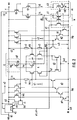
- the reference network q is designed as a fourfold bandgap circuit bg, which at the same time supplies the first and second voltage u1, u2 for determining the control deviation.
- the differential stage c and the first amplifier v1 together represent the differential device d.
- a first part of the bandgap circuit bg contains four series-connected base-emitter sections of pnp substrate transistors pt, the respective emitter area of which is determined by a value e1 specified by the design.
- a second part of the bandgap circuit bg is also made up of four base-emitter paths connected in series formed by four further pnp substrate transistors pt, the respective emitter area of which is determined by a second value e2.
- e2 is twelve times larger than e1. If all pnp substrate transistors are each supplied with the same emitter current (of, for example, 20 microamps), then a certain voltage is established at the emitter of the highest pnp substrate transistor.
- the third voltage level u3 at room temperature is approximately 256 millivolts lower than the first voltage level u1.
- the mode of operation of the bandgap circuit is known to be that the negative temperature coefficient of the base-emitter paths is compensated for by the positive temperature coefficient of a voltage which is proportional to the emitter area-dependent differential voltage u1 - u3.
- a certain voltage value is added to a voltage with a negative temperature response (absolute value), the temperature response (absolute value) of which is opposite but the same in magnitude.
- This voltage value is generally formed by supplying the differential voltage dependent on the emitter area to a voltage-current converter which is connected to a voltage converter Resistance changes the current flowing through it. The voltage difference that drops across the connected resistor has the same temperature coefficient as the emitter area-dependent differential voltage.
- the resistance value is to be specified so large that the absolute voltage value required for compensation is met exactly. In the exemplary embodiment according to FIG. 2, this is achieved by the voltage drop at the resistor r1 or by the voltage drop at the resistor series circuit r2, r3.
- the regulated supply voltage uc is therefore the actual, temperature-stabilized band gap voltage.
- the voltages u1, u2 at the two nodes k4, k5 are also of the same size, so that the voltage comparison in the control loop only requires a simple difference measurement u1 - u2.
- the slope of the characteristic curves of the two voltages u1, u2 as a function of the voltage uc are different, but the two characteristic curves intersect at a value of approximately 2.7 volts, the voltage uc having a value of approximately 5 volts, cf. Fig. 4.
- the output voltage uc of the bandgap circuit bg is readjusted until the voltage difference u1 - u2 becomes zero - the regulated supply voltage uc then has the desired value of approximately 5 volts.
- the differential device d is realized in FIG. 2 by a differential amplifier c, v1 with an active load.
- the differential input is formed by a pair of p-channel transistors, the gate electrodes of which are connected to the fourth and fifth nodes k4, k5 and the common source connection of the p-channel current source q1 is fed with the operating current iq.
- the output of the differential amplifier is formed by a seventh node k7, which lies between the output of the active load and a p-channel transistor serving as a cascode.
- the seventh node k7 supplies the control signal s1, which is fed to the inverting input of the second amplifier v2.
- the gate connection of the current source q1 is at the same bias voltage uq as the p-channel transistors that feed the bandgap circuit bg.
- the starting device st in FIG. 2 essentially consists of a current switch which is fed with a current i3 by a p-channel transistor t3.
- the respective current path is controlled by a pair of p-channel transistors t1, t2, which for the most part supplies current i3 as current i4 to a first load 11 in the first start phase p1 and completely as current i5 to a second load 12 outside the start phase.
- the first load 11 is an n-channel transistor t4 connected as a diode
- the second load 12 is the series connection of two diode paths.
- the first diode path is formed by an n-channel transistor t5 and the second diode path is formed by a pnp substrate transistor t6, the base and collector connections of which are connected to the reference potential M.
- the n-channel transistor t4 connected as a diode also forms the input of the auxiliary circuit h, which is formed from an n-channel current bank and supplies a first and second auxiliary signal x1, x2 as output signals.
- the first auxiliary signal x1 pulls the seventh node k7 and thus the inverting input of the second amplifier v2 in the direction of the reference potential M.
- the second auxiliary signal x2 is connected to a bias input of the amplifier v2 and also pulls this in the direction of the reference potential M, cf. Fig. 3. All the required cross current paths are switched through.
- the first Auxiliary signal x1 replaces the output signal s1 of the first amplifier v1 in the start-up phase.
- the first sensor f1 from FIG. 1 corresponds to the transistor pair t1, t2 in FIG. 2, the gate electrodes of which are connected to the second and fourth nodes k2, k4.
- both gate connections are almost at the reference potential M, so that the current distribution is only dependent on the resistance ratio of the first and second loads 11, 12.
- the simple diode path of the first load has a lower resistance than the series connection of the two diode paths in the second load, the current i3 supplied predominantly flows via the transistor t4 and therefore activates the auxiliary circuit h.
- the switching threshold w1 is reached and transistor t1 is blocked. Then the entire current i3 flows out via the second load 12. So that the first start phase p1 ends.
- the second sensor f2 of FIG. 1, which monitors a different operating current, corresponds in FIG. 2 to the circuit arrangement comprising the two p-channel transistors t6 and t7 connected in series.
- Transistor t6 supplies the operating current iq in the current source q1, which should flow as current iv1 in the differential amplifier c, v1.
- the source-drain path of the transistor t6 is in the unsaturated state because the differential amplifier cannot yet accept the operating current iq.
- the gate potential of transistor t6 is thus significantly lower than its drain potential uv at node kv.
- This state is recognized by the p-channel transistor t7, whose gate and source electrodes are connected to the gate and drain electrodes of the sixth transistor t6.
- the n-well of the seventh transistor t7 is also connected to the drain electrode of the sixth transistor t6.
- the saturation limit of the p-channel transistor t6 represents the second switching threshold w2, which is assigned to the second sensor device, because as long as transistor t6 is not saturated, at least part of the operating current iq flows as current i6 via the seventh transistor t7 Input of the auxiliary circuit h and activates it.
- transistor t6 saturates, transistor t7 is blocked and the entire operating current iq flows into the differential amplifier c, v1. There is therefore no activation current i6 for the auxiliary circuit h, which makes it inactive and ends the second start phase p2.
- FIG. 3 shows an advantageous exemplary embodiment for the second amplifier v2. It is a transconductance amplifier with an A / B push-pull output stage in CMOS technology. An almost identical circuit is described in detail in EP-A 0 460 263.
- the amplifier v2 has two complementary current branches, the slope of which is set to the same size by means of the circuit design.
- the control circuit ensures that the two current branches are controlled with voltages of the same size. This is achieved in that both the gate connection of the n-channel output transistor t9 and the gate connection of a p-channel transistor t10 are driven together by the first amplifier v1.
- the source connection of the transistor t10 lies at a node k9 with a fixed potential u5 and the source connection of the transistor t9 lies at the reference potential M.
- the output current of the transistor t10 is mirrored by means of an n-channel current mirror m1 and a p- Channel current mirror supplied, the output transistor of which is the output transistor t8 of the A / B push-pull output stage.
- the drain electrodes of the eighth and ninth transistors t8 and t9 are connected to one another and form the second circuit node k2.
- the transistors t9, t10 must also have the same slope, a transmission ratio of the two current mirrors m1, m2 which deviates from 1 having to be taken into account.
- the first amplifier v1 is fed by a differential voltage u4, which corresponds, for example, to the differential voltage between the fourth and fifth nodes k4, k5 of FIG. 2.
- the bias voltage source bq controls, with its bias voltage uq ', a p-channel transistor t11 which feeds two diode paths connected in series via an eighth node k8 and thereby generates a reference voltage u5 for the fixed potential at node k9. Since the reference voltage u5 cannot be loaded, a compensating current ia flowing between the nodes k8 and k9 is compensated by an output current ia 'of the same size of a one-to-one positive feedback circuit, which is implemented by means of the two current mirrors m1, m2.
- the associated current conversion ratios are given in FIG. 3 as numerical values. It can also be seen from this that the slope of the transistor t9 must be six times greater than the slope of the transistor t10.
- the start-up behavior of the second amplifier v2 shown in FIG. 3 is not ensured without the second auxiliary signal x2.
- the direct current path for the reference voltage u5 would be blocked, for example.
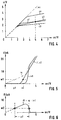
- Fig. 4 shows a schematic representation of some voltage diagrams of the embodiment of Fig. 2.
- the voltages u1, u2 and u3 of the bandgap circuit bg have up to an ordinate value u of about 2.0 volts almost the same value as the abscissa Voltage uc. This means that up to this value no currents i1, i2 flow through the resistors r1 or r2, r3 and the bandgap circuit is inactive.
- At higher abscissa values uc there is an approximately constant differential voltage between the characteristic curve u1 and u3, which is determined by the area ratio e1 / e2 of the emitters according to the formula given.
- the diagram of FIG. 4 also shows the voltage curve u2 at node k5.
- the voltage profile u1 has a smaller gradient than the voltage profile u2.
- Both voltages intersect at an ordinate value u of approx. 2.7 volts, which is assigned an abscissa value uc of approx. 5 volts - this is the actual bandgap output voltage, which is the setpoint of the regulated supply voltage uc.
- the diagram according to FIG. 4 also contains the voltage curve uv at the node kv. Up to 3.5 volts, the voltage uv is identical to the abscissa value uc, that is to say that in this region the voltage of transistor t6 is in the unsaturated state and no current iv1 flows into the differential amplifier c, v1. This can be seen more clearly in FIG. 5.
- FIG. 5 shows schematically some current diagrams of the exemplary embodiment according to FIG. 2.
- the currents i1, i2 of the bandgap circuit have the value zero at low voltages uc and only rise above a voltage uc of approximately 2.3 volts - this corresponds to the series circuit of four base emitter paths - linear on.
- the differential amplifier c, v1 is still in the de-energized state in this voltage range uc. It only becomes active from a voltage uc of about 3.5 volts, so that it can take over part of the current iq supplied from the current source q1 as current iv1.
- the current transfer does not take place abruptly, but in a transition area that ends at an abscissa value uc of approximately 4 volts. From this voltage value, the current iq supplied by the current source is completely taken over by the differential amplifier.
- the first switching threshold w1 which monitors one of the cross currents i1, i2 of the bandgap circuit bg and thus defines the first start phase p1, in no way ensures that the differential amplifier c, v1 is in the regular operating range. 5 shows that, in the worst case, the first switching threshold w1 can drop to an abscissa value uc of 2.3 V, at which the differential amplifier does not absorb any current at all.
- the differential current i6 is fed to the starting device st and defines the second starting phase p2 via the second switching threshold w2, which ends approximately at an abscissa value uc of approximately 3.8 volts. Since the second switching threshold w2 falls below the differential current i6 even at a low voltage uc, a combination and thus overlap of the first and second starting phases p1, p2 is necessary. This takes place in the Starting device st of FIG. 2 by adding the currents i4 and i6 in the input of the auxiliary circuit h.
Landscapes
- Engineering & Computer Science (AREA)
- Physics & Mathematics (AREA)
- Electromagnetism (AREA)
- General Physics & Mathematics (AREA)
- Radar, Positioning & Navigation (AREA)
- Automation & Control Theory (AREA)
- Power Engineering (AREA)
- Amplifiers (AREA)
- Continuous-Control Power Sources That Use Transistors (AREA)
Applications Claiming Priority (2)
| Application Number | Priority Date | Filing Date | Title |
|---|---|---|---|
| DE4242989A DE4242989C1 (de) | 1992-12-18 | 1992-12-18 | Spannungsregler |
| DE4242989 | 1992-12-18 |
Publications (3)
| Publication Number | Publication Date |
|---|---|
| EP0602466A2 true EP0602466A2 (fr) | 1994-06-22 |
| EP0602466A3 EP0602466A3 (fr) | 1995-03-29 |
| EP0602466B1 EP0602466B1 (fr) | 1998-03-04 |
Family
ID=6475783
Family Applications (1)
| Application Number | Title | Priority Date | Filing Date |
|---|---|---|---|
| EP93119431A Expired - Lifetime EP0602466B1 (fr) | 1992-12-18 | 1993-12-02 | Régulateur de tension integré monolithique |
Country Status (4)
| Country | Link |
|---|---|
| US (1) | US5446380A (fr) |
| EP (1) | EP0602466B1 (fr) |
| JP (1) | JPH06274234A (fr) |
| DE (2) | DE4242989C1 (fr) |
Families Citing this family (7)
| Publication number | Priority date | Publication date | Assignee | Title |
|---|---|---|---|---|
| DE4334513C1 (de) * | 1993-10-09 | 1994-10-20 | Itt Ind Gmbh Deutsche | CMOS-Schaltung mit erhöhter Spannungsfestigkeit |
| DE4431466C1 (de) * | 1994-05-31 | 1995-06-08 | Itt Ind Gmbh Deutsche | Spannungsregler |
| US5510699A (en) * | 1994-05-31 | 1996-04-23 | Deutsche Itt Industries Gmbh | Voltage regulator |
| JP3456904B2 (ja) * | 1998-09-16 | 2003-10-14 | 松下電器産業株式会社 | 突入電流抑制手段を備えた電源回路、およびこの電源回路を備えた集積回路 |
| US6384582B2 (en) | 2000-05-19 | 2002-05-07 | Endress + Hauser Flowtec Ag | Controlled current sources of two-wire measuring instruments |
| EP1158274B1 (fr) * | 2000-05-19 | 2009-02-18 | Endress + Hauser Flowtec AG | Sources de courant controllées pour mesureurs bifilaires |
| JP3680784B2 (ja) * | 2001-11-12 | 2005-08-10 | 株式会社デンソー | 電源回路 |
Family Cites Families (11)
| Publication number | Priority date | Publication date | Assignee | Title |
|---|---|---|---|---|
| US3401335A (en) * | 1966-03-18 | 1968-09-10 | Hewlett Packard Co | Meter circuit for power supply |
| US3549983A (en) * | 1968-06-18 | 1970-12-22 | Union Carbide Corp | High efficiency high power d.c. series type voltage regulator |
| DE2708021C3 (de) * | 1977-02-24 | 1984-04-19 | Eurosil GmbH, 8000 München | Schaltungsanordnung in integrierter CMOS-Technik zur Regelung der Speisespannung für eine Last |
| GB2034937B (en) * | 1978-11-14 | 1983-01-06 | Philips Electronic Associated | Regulated power supply |
| DE3010618A1 (de) * | 1980-03-20 | 1981-09-24 | Robert Bosch Gmbh, 7000 Stuttgart | Schaltungsanordnung zum konstanthalten einer versorgungsspannung |
| JPS61244058A (ja) * | 1985-04-22 | 1986-10-30 | プレシジヨン・モノリシツクス・インコ−ポレ−テツド | バンドギヤツプ電圧基準回路 |
| US4952867A (en) * | 1986-03-12 | 1990-08-28 | Beltone Electronics Corporation | Base bias current compensator |
| NL8601395A (nl) * | 1986-05-30 | 1987-12-16 | At & T & Philips Telecomm | Gelijkspanningsomzetter met overbelastingbeveiliging. |
| EP0460263B1 (fr) * | 1990-06-07 | 1996-08-28 | Deutsche ITT Industries GmbH | Etage de sortie linéaire réalisé en technologie CMOS |
| DE59010535D1 (de) * | 1990-12-22 | 1996-11-14 | Itt Ind Gmbh Deutsche | Spannungsregler mit einem CMOS-Transkonduktanzverstärker mit gleitendem Arbeitspunkt |
| DE4111103A1 (de) * | 1991-04-05 | 1992-10-08 | Siemens Ag | Cmos-bandabstands-referenzschaltung |
-
1992
- 1992-12-18 DE DE4242989A patent/DE4242989C1/de not_active Expired - Fee Related
-
1993
- 1993-12-02 EP EP93119431A patent/EP0602466B1/fr not_active Expired - Lifetime
- 1993-12-02 DE DE59308207T patent/DE59308207D1/de not_active Expired - Lifetime
- 1993-12-09 US US08/164,188 patent/US5446380A/en not_active Expired - Lifetime
- 1993-12-20 JP JP5320526A patent/JPH06274234A/ja active Pending
Also Published As
| Publication number | Publication date |
|---|---|
| US5446380A (en) | 1995-08-29 |
| DE59308207D1 (de) | 1998-04-09 |
| DE4242989C1 (de) | 1994-05-11 |
| JPH06274234A (ja) | 1994-09-30 |
| EP0602466B1 (fr) | 1998-03-04 |
| EP0602466A3 (fr) | 1995-03-29 |
Similar Documents
| Publication | Publication Date | Title |
|---|---|---|
| DE3523400C2 (de) | Schaltungsanordnung für eine Ausgangsstufe der Klasse AB mit großer Schwingungsweite | |
| DE69011756T2 (de) | Stromspiegelschaltung. | |
| DE3625949C2 (de) | Schaltung zum Erzeugen eines stabilisierten Stromes, insbesondere für integrierte MOS-Schaltungen | |
| EP0483537B1 (fr) | Circuit de source de courant | |
| DE68927535T2 (de) | Verstärker | |
| DE3713107C2 (de) | Schaltung zur Erzeugung von konstanten Spannungen in CMOS-Technologie | |
| EP0491980B1 (fr) | Regulateur de tension avec amplificateur CMOS de transconductance avec polarisation glissante | |
| EP0529118B1 (fr) | Circuit de régulation de courant | |
| DE69416610T2 (de) | Integrierter, differentieller, die Abschwächung durch Hochspannungstransistoren nutzender Hochspannungssensor | |
| DE69020748T2 (de) | Differenzverstärker mit Spannungsverschiebung zur Erzielung einer Eingangsfähigkeit über den ganzen, sehr niedrigen Versorgungsspannungsbereich. | |
| DE69118693T2 (de) | Differenzverstärkeranordnung | |
| EP0508327A2 (fr) | Circuit de référence du type Bandgap | |
| DE102019209071A1 (de) | Spannungsgenerator | |
| DE2254618B2 (de) | Integrierte spannungsregelschaltung | |
| DE69403776T2 (de) | Cmos-operationsverstärker mit verbesserter leistung über den gesamten speisespannungsbereich | |
| DE69623754T2 (de) | Spannungsregler mit schneller Reaktionszeit und niedrigem Verbrauch und dazugehöriges Verfahren | |
| DE4133902A1 (de) | Cmos-leistungsverstaerker | |
| DE68921136T2 (de) | Transistorverstärker für hohe Anstiegsgeschwindigkeiten und kapazitive Belastungen. | |
| DE19735381C1 (de) | Bandgap-Referenzspannungsquelle und Verfahren zum Betreiben derselben | |
| DE69517706T2 (de) | Verstärker | |
| DE4242989C1 (de) | Spannungsregler | |
| EP0360888A1 (fr) | Modulateur CMOS d'impulsions en durée | |
| DE2631916A1 (de) | Polarisationsanordnung fuer differenzverstaerker | |
| EP1101279B1 (fr) | Etage de sortie d'amplificateur | |
| DE69317240T2 (de) | Eingangs-Verstärkerschaltung |
Legal Events
| Date | Code | Title | Description |
|---|---|---|---|
| PUAI | Public reference made under article 153(3) epc to a published international application that has entered the european phase |
Free format text: ORIGINAL CODE: 0009012 |
|
| AK | Designated contracting states |
Kind code of ref document: A2 Designated state(s): DE FR GB IT NL |
|
| PUAL | Search report despatched |
Free format text: ORIGINAL CODE: 0009013 |
|
| AK | Designated contracting states |
Kind code of ref document: A3 Designated state(s): DE FR GB IT NL |
|
| 17P | Request for examination filed |
Effective date: 19950812 |
|
| GRAG | Despatch of communication of intention to grant |
Free format text: ORIGINAL CODE: EPIDOS AGRA |
|
| 17Q | First examination report despatched |
Effective date: 19970417 |
|
| GRAG | Despatch of communication of intention to grant |
Free format text: ORIGINAL CODE: EPIDOS AGRA |
|
| GRAG | Despatch of communication of intention to grant |
Free format text: ORIGINAL CODE: EPIDOS AGRA |
|
| GRAH | Despatch of communication of intention to grant a patent |
Free format text: ORIGINAL CODE: EPIDOS IGRA |
|
| GRAH | Despatch of communication of intention to grant a patent |
Free format text: ORIGINAL CODE: EPIDOS IGRA |
|
| GRAA | (expected) grant |
Free format text: ORIGINAL CODE: 0009210 |
|
| RAP1 | Party data changed (applicant data changed or rights of an application transferred) |
Owner name: MICRONAS INTERMETALL GMBH |
|
| AK | Designated contracting states |
Kind code of ref document: B1 Designated state(s): DE FR GB IT NL |
|
| ITF | It: translation for a ep patent filed | ||
| REF | Corresponds to: |
Ref document number: 59308207 Country of ref document: DE Date of ref document: 19980409 |
|
| ET | Fr: translation filed | ||
| GBT | Gb: translation of ep patent filed (gb section 77(6)(a)/1977) |
Effective date: 19980331 |
|
| PLBE | No opposition filed within time limit |
Free format text: ORIGINAL CODE: 0009261 |
|
| STAA | Information on the status of an ep patent application or granted ep patent |
Free format text: STATUS: NO OPPOSITION FILED WITHIN TIME LIMIT |
|
| 26N | No opposition filed | ||
| REG | Reference to a national code |
Ref country code: GB Ref legal event code: IF02 |
|
| PGFP | Annual fee paid to national office [announced via postgrant information from national office to epo] |
Ref country code: NL Payment date: 20091222 Year of fee payment: 17 |
|
| PGFP | Annual fee paid to national office [announced via postgrant information from national office to epo] |
Ref country code: IT Payment date: 20091218 Year of fee payment: 17 |
|
| REG | Reference to a national code |
Ref country code: NL Ref legal event code: V1 Effective date: 20110701 |
|
| PG25 | Lapsed in a contracting state [announced via postgrant information from national office to epo] |
Ref country code: IT Free format text: LAPSE BECAUSE OF NON-PAYMENT OF DUE FEES Effective date: 20101202 Ref country code: NL Free format text: LAPSE BECAUSE OF NON-PAYMENT OF DUE FEES Effective date: 20110701 |
|
| REG | Reference to a national code |
Ref country code: DE Ref legal event code: R084 Ref document number: 59308207 Country of ref document: DE Effective date: 20110204 |
|
| PGFP | Annual fee paid to national office [announced via postgrant information from national office to epo] |
Ref country code: GB Payment date: 20121220 Year of fee payment: 20 |
|
| PGFP | Annual fee paid to national office [announced via postgrant information from national office to epo] |
Ref country code: DE Payment date: 20121220 Year of fee payment: 20 Ref country code: FR Payment date: 20130130 Year of fee payment: 20 |
|
| REG | Reference to a national code |
Ref country code: DE Ref legal event code: R071 Ref document number: 59308207 Country of ref document: DE |
|
| REG | Reference to a national code |
Ref country code: GB Ref legal event code: PE20 Expiry date: 20131201 |
|
| PG25 | Lapsed in a contracting state [announced via postgrant information from national office to epo] |
Ref country code: GB Free format text: LAPSE BECAUSE OF EXPIRATION OF PROTECTION Effective date: 20131201 Ref country code: DE Free format text: LAPSE BECAUSE OF EXPIRATION OF PROTECTION Effective date: 20131203 |