EP0602568A2 - Structure à multi-couches ayant une couche tampon à orientation (111) - Google Patents
Structure à multi-couches ayant une couche tampon à orientation (111) Download PDFInfo
- Publication number
- EP0602568A2 EP0602568A2 EP93119988A EP93119988A EP0602568A2 EP 0602568 A2 EP0602568 A2 EP 0602568A2 EP 93119988 A EP93119988 A EP 93119988A EP 93119988 A EP93119988 A EP 93119988A EP 0602568 A2 EP0602568 A2 EP 0602568A2
- Authority
- EP
- European Patent Office
- Prior art keywords
- substrate
- buffer layer
- multilayer structure
- group
- superlattice
- Prior art date
- Legal status (The legal status is an assumption and is not a legal conclusion. Google has not performed a legal analysis and makes no representation as to the accuracy of the status listed.)
- Withdrawn
Links
Images

Classifications
-
- G—PHYSICS
- G02—OPTICS
- G02F—OPTICAL DEVICES OR ARRANGEMENTS FOR THE CONTROL OF LIGHT BY MODIFICATION OF THE OPTICAL PROPERTIES OF THE MEDIA OF THE ELEMENTS INVOLVED THEREIN; NON-LINEAR OPTICS; FREQUENCY-CHANGING OF LIGHT; OPTICAL LOGIC ELEMENTS; OPTICAL ANALOGUE/DIGITAL CONVERTERS
- G02F1/00—Devices or arrangements for the control of the intensity, colour, phase, polarisation or direction of light arriving from an independent light source, e.g. switching, gating or modulating; Non-linear optics
- G02F1/35—Non-linear optics
- G02F1/37—Non-linear optics for second-harmonic generation
-
- C—CHEMISTRY; METALLURGY
- C30—CRYSTAL GROWTH
- C30B—SINGLE-CRYSTAL GROWTH; UNIDIRECTIONAL SOLIDIFICATION OF EUTECTIC MATERIAL OR UNIDIRECTIONAL DEMIXING OF EUTECTOID MATERIAL; REFINING BY ZONE-MELTING OF MATERIAL; PRODUCTION OF A HOMOGENEOUS POLYCRYSTALLINE MATERIAL WITH DEFINED STRUCTURE; SINGLE CRYSTALS OR HOMOGENEOUS POLYCRYSTALLINE MATERIAL WITH DEFINED STRUCTURE; AFTER-TREATMENT OF SINGLE CRYSTALS OR A HOMOGENEOUS POLYCRYSTALLINE MATERIAL WITH DEFINED STRUCTURE; APPARATUS THEREFOR
- C30B23/00—Single-crystal growth by condensing evaporated or sublimed materials
- C30B23/02—Epitaxial-layer growth
-
- C—CHEMISTRY; METALLURGY
- C30—CRYSTAL GROWTH
- C30B—SINGLE-CRYSTAL GROWTH; UNIDIRECTIONAL SOLIDIFICATION OF EUTECTIC MATERIAL OR UNIDIRECTIONAL DEMIXING OF EUTECTOID MATERIAL; REFINING BY ZONE-MELTING OF MATERIAL; PRODUCTION OF A HOMOGENEOUS POLYCRYSTALLINE MATERIAL WITH DEFINED STRUCTURE; SINGLE CRYSTALS OR HOMOGENEOUS POLYCRYSTALLINE MATERIAL WITH DEFINED STRUCTURE; AFTER-TREATMENT OF SINGLE CRYSTALS OR A HOMOGENEOUS POLYCRYSTALLINE MATERIAL WITH DEFINED STRUCTURE; APPARATUS THEREFOR
- C30B29/00—Single crystals or homogeneous polycrystalline material with defined structure characterised by the material or by their shape
- C30B29/60—Single crystals or homogeneous polycrystalline material with defined structure characterised by the material or by their shape characterised by shape
- C30B29/68—Crystals with laminate structure, e.g. "superlattices"
-
- G—PHYSICS
- G02—OPTICS
- G02B—OPTICAL ELEMENTS, SYSTEMS OR APPARATUS
- G02B6/00—Light guides; Structural details of arrangements comprising light guides and other optical elements, e.g. couplings
- G02B6/10—Light guides; Structural details of arrangements comprising light guides and other optical elements, e.g. couplings of the optical waveguide type
- G02B6/12—Light guides; Structural details of arrangements comprising light guides and other optical elements, e.g. couplings of the optical waveguide type of the integrated circuit kind
- G02B6/13—Integrated optical circuits characterised by the manufacturing method
- G02B6/131—Integrated optical circuits characterised by the manufacturing method by using epitaxial growth
Definitions
- This invention relates to multilayer structures, including a semiconductor substrate, which are suitable for use in electronic, optical or electro-optic applications.
- This invention more particularly relates to a multilayer structure having as layers: a single crystal (111)-oriented semiconductor substrate and an epitaxial buffer layer having a three-fold rotation symmetry about the substrate (111) direction.
- NLO nonlinear optical
- LiNb x Ta 1-x O3 LiNb x Ta 1-x O3, where x is a number from 0 to 1 (referred to herein as "LiNb x Ta 1-x O3") have large nonlinear susceptibilities and transparency from 350nm-4000nm and these materials are commonly used for blue light generation in the form of bulk crystals. LiNb x Ta 1-x O3 can also be provided in the form of thin films. For blue light generation with high efficiency, the LiNb x Ta 1-x O3 NLO film and adjoining materials should form a waveguide, in which layers adjoining the nonlinear optical thin film, have lower refractive indexes than the film. Kanata, T.
- LiNbO3 and LiTaO3 films on sapphire substrates provide a multilayer structure, however, that structure lacks a semiconductor suitable for monolithic integration.
- a single chip would include, for example; diode lasers, frequency doublers, light detectors and necessary electronics.
- Substrates suitable for monolithic integration include Si and GaAs.
- GaAs is not suitable for use as an optical buffer, since it has a very high refractive index and absorbs in the visible range. GaAs reacts with LiNb x Ta 1-x O3 at interfaces to produce undesirable phases.
- Metal oxides such as ZrO2, PrO2, CeO2, Al2O3, MgAl2O4 and MgO have been reported to grow epitaxially on Si substrates.
- ZrO2, PrO2, CeO2, and MgAl2O4 are unsuitable for use as a buffer layer between GaAs and an NLO film of LiTaO3 or the like.
- CeO2 and PrO2 have excessive optical absorption.
- ZrO2 is transparent, but has a large refractive index.
- MgAl2O4 is colorless and has a low refractive index, but has too high a deposition temperature for use with GaAs.
- Orientation of epitaxial metal oxide buffer layers matches the orientation of the substrate in some cases, but not in others.
- a multilayer structure comprising in order: a (111)-oriented single crystal substrate and an epitaxial metal oxide buffer layer.
- the substrate is doped or undoped.
- the substrate is a semiconductor selected from the group consisting of Si compounds, Ge compounds, and compounds having at least one element selected from the group consisting of Al, Ga, and In and at least one element selected from the group consisting of N, P, As, and Sb.
- the substrate defines a substrate superlattice dimension equal to 3 times a sublattice constant of the substrate.
- the epitaxial metal oxide buffer layer has a three-fold rotation symmetry about the substrate (111) direction.
- the buffer layer defines a buffer layer superlattice dimension equal to 4 times the oxygen-to-oxygen lattice spacing of the buffer layer.
- the buffer layer superlattice dimension is within 15 percent of the substrate superlattice dimension.
- an epitaxial buffer layer having a three-fold rotation symmetry about the substrate (111) direction can be provided on a a single crystal (111)-oriented semiconductor substrate.
- a multilayer structure 10 of the invention has, in order, a substrate 11 and a buffer layer 13.
- an alternative embodiment of the multilayer structure 10 of the invention has, in addition to substrate 11 and buffer layer 13, an upper layer 15 overlaying buffer layer 13.
- Substrate 11 is a (111)-oriented single crystal semiconductor substrate.
- Substrate is (111)GaAs or, alternatively, substrate 11 is a (111)-oriented semiconductor selected from compounds of the Group IVa elements Si and Ge or selected from Group IIIa-Group Va compounds having at least one Group IIIa element selected from Al, Ga, and In and at least one Group Va element selected from N, P, As, and Sb.
- substrate 11 is a semiconductor selected from the group consisting of Si, Ge, GaP, InAs, GaSb, InSb, InP, Si x Ge 1-x , and Al x Ga 1-x As, where x is from 0 to 1.
- Each of the semiconductors listed in Table 1 has an equivalent crystal structure to GaAs in terms of epitaxy, ZnS(zinc blende or diamond), and a small lattice constant mismatch to GaAs of less than 8 percent.
- Substrate 11 can be an undoped, lightly doped or heavily doped semiconductor. In some circumstances a doped semiconductor is more desirable because an electrode can be provided beneath the buffer layer. Such an electrode would lower electro-optic device voltage requirements, where an electric field is applied normal to the substrate surface. Suitable dopants include, for a Group IVa compound: As, P, B, Sb, and Bi and for a Group IIIa-Group Va compound: Si, Ge, Zn, and Mg. Substrate 11 may be doped everywhere or only in selected areas on the substrate surface. In some applications, part of the semiconductor can be used as substrate 11 for multilayer structure 10, while the remainder of the semiconductor wafer can be processed to form laser diodes or other electronic devices.
- Epitaxial metal oxide buffer layer 13 has a three-fold rotation symmetry, or both three-fold and six-fold rotation symmetry, about the substrate ⁇ 111 ⁇ direction, that is buffer layer 13 has the same rotation symmetry as substrate 11, about the surface normal of substrate 11.
- Suitable metal oxides include: (111)MgO, (0001)Al2O3, (0001)Ga2O3, and (111)SrTiO3.
- Buffer layer 13 is stable at high temperatures and acts as a diffusion buffer between substrate and an overlying film, for example, a nonlinear optical (NLO) upper layer 15.
- the thickness of buffer layer 13 is selected so as to be sufficient to provide this function.
- the material of buffer layer 13 is selected to meet a particular purpose.
- SrTiO3 is not suitable for supporting waveguides because of its high refractive index, but is useful for the growth of various non-optical materials.
- the diffusion buffer 13 also has to be transparent over a wide range of wavelengths in addition to having a lower refractive index than the nonlinear optical film. MgO, Ga2O3 and Al2O3 are suitable for this purpose.
- the thickness should be such that the strength of the evanescent tail of the mode of the wave propagating in the waveguide is negligible at the interface of substrate 11 and buffer layer 13.
- a sufficient thickness ranges from 30 to 3000nm, preferably 200-2000nm; most preferably about 500-1500nm.
- Buffer layer 13 can be grown epitaxially by many conventional means, such as laser ablation, electron beam and chemical vapor deposition.
- the structural relationship between buffer layer and substrate can be described in terms of a pair of superlattices defined by the two materials. The presence of these two superlattices allows for epitaxy of what would be considered otherwise to be unlike crystal structures.
- the substrate superlattice cell is composed of 3 cells of the substrate lattice.
- a substrate superlattice dimension can be defined as being equal to 3 times a sublattice constant of the substrate. For (111)GaAs the sublattices are Ga and As and the sublattice constant is 4.00 Angstroms. The superlattice dimension for GaAs is thus 12.00.
- Buffer layer 13 has a superlattice cell composed of four cells of the metal oxide buffer layer lattice.
- the buffer layer superlattice dimension is equal to 4 times the oxygen-to-oxygen lattice spacing of buffer layer 13.
- the O-O spacing is 2.98 Angstroms and the superlattice dimension is 11.92.
- the percentage difference between substrate and buffer layer superlattice dimensions is referred to herein as superlattice mismatch.
- (111)MgO has a superlattice mismatch of -0.67 percent to (111)GaAs. Symmetries, O-O spacings, and mismatches for a variety of metal oxides are presented in Table 2.
- Buffer layer 13 acts as a seed for the epitaxial growth of upper layer 15.
- An oxide upper layer 15 can be grown by any conventional methods, such as rf-sputtering, electron-beam evaporation, laser ablation and metal organic chemical vapor deposition.
- Suitable metal oxides for upper layer 15 have either 3-fold or 6-fold rotation symmetry about the substrate ⁇ 111 ⁇ direction.
- suitable upper layer oxides include: BaFe12O18 and LiNb x Ta 1-x O3 (0 ⁇ x ⁇ 1).
- LiNb x Ta 1-x O3 which includes LiNbO3 and LiTaO3, exhibits substantial nonlinear optical effects.
- LiNb x Ta 1-x O3 crystals have three-fold rotational symmetry about the ⁇ 0001 ⁇ direction, alternatively called the c-axis, and thus belong to the trigonal system; in addition, LiNb x Ta 1-x O3 crystals exhibit mirror symmetry about three planes that are 60° apart. These two symmetry operations classify LiNbO3, LiTaO3 and other LiNb x Ta 1-x O3 compounds as members of the 3m point group, and can be referred to as conventional hexagonal unit cells.
- upper layer 15 oxides exhibit an oxygen-to-oxygen sublattice, which has a mismatch to the buffer layer 13 oxygen-to-oxygen sublattice of less than 15 percent and preferably less than 10 percent.
- Upper layer 15 and buffer layer 13 need not exhibit the same structure.
- substrate 11 can have the diamond or zinc blende structure
- buffer layer 13 can be simple cubic
- upper layer can be trigonal or hexagonal.
- the multilayer structure 10 of the invention is produced by epitaxially growing buffer layer 13 on substrate 11, followed by epitaxially growing upper layer 15 on buffer layer 13.
- multilayer structure 10 is produced by epitaxially growing an (111)MgO buffer layer, on (NH4)2S x -treated GaAs substrate 11, by electron-beam evaporation.
- a LiNb x Ta 1-x O3 (0 ⁇ x ⁇ 1) upper layer is then epitaxially grown by pulsed laser deposition on the MgO buffer layer.
- a suitable substrate heater temperature for the growth of the upper layer is 525°C to 750°C.
- (111)GaAs wafers were first etched for use as substrates. After a conventional cleaning in organic solvents, the wafers were etched in a solution with 1 part of H2SO4, 8 parts of H2O2, and 500 parts of H2O for 30 seconds, followed by a deionized water rinse. Prior to being loaded in an evaporator, the samples were placed in a saturated (NH4)2S x solution for 3 to 5 minutes. Following this soak, the ammonium sulfide solution was diluted with deionized water and the samples were immersed in a diluted solution for 3 to 5 minutes before being dried under a stream of nitrogen. This etching method allows the growth of epitaxial films on GaAs without in situ thermal etching or sputter cleaning.
- a buffer layer of MgO with a thickness of 100 nm was deposited on the (NH4)2S x -treated (111)GaAs substrate at 550°C by electron-beam evaporation.
- the deposition process was carried out at 3 x 10 ⁇ 8 Torr without introducing additional oxygen into the system, to ensure an undisturbed GaAs surface prior to the growth of epitaxial MgO film.
- the substrate was heated by a radiative heater consisting of tantalum wires.
- the growth temperature was 400°C to 550°C and monitored by an infrared pyrometer using published emissivity values.
- the deposition rate was 0.05-0.15 nm/s and the thickness of the MgO buffer layer was between 100 and 500 nm.
- LiTaO3 upper layers were grown by pulsed laser ablation.
- a laser pulse energy of 360 mJ with a 30 ns duration and a pulse rate of 4 Hz was generated by a KrF excimer laser.
- the beam was focused to a 5mm2 spot onto a target of polycrystalline LiTaO3.
- the multilayer structure (MgO buffer layer/GaAs substrate) was located 6 cm from the target and heated to 560°C by a resistive heater. The temperature was monitored by a thermocouple attached to an inner wall of the heater block.
- the deposition was carried out at a rate of 0.1 nm/pulse under an oxygen pressure of 92 mTorr to provide a multilayer structure of the invention having an upper layer of LiTaO3 having a thickness of 400 nm.
- the sample was then cooled to room temperature with oxygen flowing at a pressure of 150 Torr.
- Theta-2-theta x-ray diffraction was conducted to determine the distribution of the crystal orientation with respect to the substrate surface normal.
- only lattice planes parallel to the substrate surface will be detected; this means for single-crystalline films that strong lines are detected only if a major crystallographic direction is aligned with the substrate surface.
- Rocking curves were measured with a stationary detector positioned at an appropriate diffraction angle 2-theta by tilting the sample through a suitable angle range.
- X-ray pole figure measurements were taken to examine in-plane orientation.
- a beam of monochromatic x-radiation is diffracted from a thin film, and the sample is tilted to such a degree that a selected set of parallel crystallographic planes meet the Bragg condition.
- the film is then rotated about an axis normal to the substrate.
- Detected diffraction over a wide range of rotation angles indicates a distribution of in-plane orientations.
- azimuth angles indicates a distribution of in-plane orientations.
- azimuth angles Detected diffraction over a wide range of rotation angles
- ideal alignment is seen as three spot reflections separated one from the other by a 120° rotation angle.
- a poor in-plane alignment corresponds to a large number of individual microcrystalline film segments (referred to as grains) separated by high angle intergrain boundaries, that could lower critical current densities in superconductors or increase light scattering in optical materials.
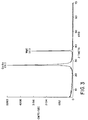
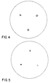
- Figure 3 is an x-ray diffraction pattern and Figures 4 and 5 are pole patterns, taken prior to deposition of the NLO upper layer 15. Only the peak corresponding to the MgO(111) plane was observed. X-ray rocking curve analysis showed the full-width at half maximum (FWHM) of the (111) line was about 2.2°, indicating a highly (111)-oriented film. Crystal orientation in the (111) plane was examined by pole figure measurements.
- Figure 4 is a pole figure of the MgO(200) planes. Three spot-like pole densities were found every 120°, indicating a good in-plane alignment.
- Figure 5 is a pole figure of the (200)plane of the underlying GaAs substrate.
- the figure shows excellent in-plane alignment as expected for high-quality single crystal GaAs wafers.
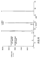
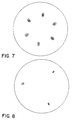
- Figure 6 is an x-ray diffraction pattern and Figures 7 and 8 are pole patterns, taken after the LiTaO3 upper layer was deposited.
- Figure 6 clearly shows both the (111) orientation of the MgO buffer layer and the (0006) orientation of the LiTaO3 film.
- the FWHM of the LiTaO3(0006) rocking curve measured 2.1°.
- This c-axis orientation of LiTaO3 is highly desirable for electro-optic or nonlinear optical applications.
- the in-plane orientation of the LiTaO3 film was determined with the pole figure of Figure 7. The analysis was performed for the (01-12) plane of LiTaO3 and clearly shows in-plane orientation.
- LiTaO3 belongs to the 3m crystal class and exhibits a three fold rotation symmetry about the c-axis, which leads to three spots in the pole figure.
- Figure 7 shows six spots indicating that the film was twinned in-plane. However, this twinned structure would not affect the refractive index, nonlinear susceptibility and light scattering.
- Figure 8 is a pole figure of the (200) plane of the underlying GaAs substrate. A comparison of the results obtained from LiTaO3 and that from the underlying GaAs in Fig. 8 indicated that a c-oriented LiTaO3 film was grown epitaxially on (111) GaAs with an in-plane alignment of LiTaO3 [1100] parallel to GaAs [110].
- Rutherford backscattering spectrometry was conducted on the multilayer structure and provided the spectrum shown in Fig. 9.
- the peak centered at 1.76 MeV corresponds to Ta in the surface layer.
- the peak appearing at 0.86 MeV is due to overlapping Mg and GaAs signals.
- the step observed at energies below 0.71 MeV is attributable to helium ions scattered from oxygen.
- the spectrum can be best fitted by a simulation of a bilayered structure with the stoichiometric ration of 1.0 Mg to 1.0 Oxygen and of 1.15 Li to 0.97 Ta to 3 Oxygen.
- the rear edge of the Ta profile and the front edge of the GaAs profile are abrupt, indicating limited interfacial reaction.
- the invention may be summarized as follows:
Landscapes
- Physics & Mathematics (AREA)
- Chemical & Material Sciences (AREA)
- Engineering & Computer Science (AREA)
- Nonlinear Science (AREA)
- General Physics & Mathematics (AREA)
- Organic Chemistry (AREA)
- Metallurgy (AREA)
- Materials Engineering (AREA)
- Optics & Photonics (AREA)
- Crystallography & Structural Chemistry (AREA)
- Microelectronics & Electronic Packaging (AREA)
- Crystals, And After-Treatments Of Crystals (AREA)
- Optical Integrated Circuits (AREA)
- Electrodes Of Semiconductors (AREA)
- Semiconductor Lasers (AREA)
- Recrystallisation Techniques (AREA)
Applications Claiming Priority (2)
| Application Number | Priority Date | Filing Date | Title |
|---|---|---|---|
| US07/992,213 US5347157A (en) | 1992-12-17 | 1992-12-17 | Multilayer structure having a (111)-oriented buffer layer |
| US992213 | 1992-12-17 |
Publications (2)
| Publication Number | Publication Date |
|---|---|
| EP0602568A2 true EP0602568A2 (fr) | 1994-06-22 |
| EP0602568A3 EP0602568A3 (fr) | 1994-12-28 |
Family
ID=25538050
Family Applications (1)
| Application Number | Title | Priority Date | Filing Date |
|---|---|---|---|
| EP93119988A Withdrawn EP0602568A3 (fr) | 1992-12-17 | 1993-12-10 | Structure à multi-couches ayant une couche tampon à orientation (111). |
Country Status (3)
| Country | Link |
|---|---|
| US (1) | US5347157A (fr) |
| EP (1) | EP0602568A3 (fr) |
| JP (1) | JPH06244407A (fr) |
Cited By (9)
| Publication number | Priority date | Publication date | Assignee | Title |
|---|---|---|---|---|
| US6392257B1 (en) | 2000-02-10 | 2002-05-21 | Motorola Inc. | Semiconductor structure, semiconductor device, communicating device, integrated circuit, and process for fabricating the same |
| WO2002008806A3 (fr) * | 2000-07-21 | 2002-06-27 | Motorola Inc | Systeme optique monolithique |
| US6583034B2 (en) | 2000-11-22 | 2003-06-24 | Motorola, Inc. | Semiconductor structure including a compliant substrate having a graded monocrystalline layer and methods for fabricating the structure and semiconductor devices including the structure |
| US6585424B2 (en) | 2001-07-25 | 2003-07-01 | Motorola, Inc. | Structure and method for fabricating an electro-rheological lens |
| US6594414B2 (en) | 2001-07-25 | 2003-07-15 | Motorola, Inc. | Structure and method of fabrication for an optical switch |
| WO2002011254A3 (fr) * | 2000-07-31 | 2003-07-31 | Motorola Inc | Structure laser a large gamme de longueurs d'ondes |
| US6693298B2 (en) | 2001-07-20 | 2004-02-17 | Motorola, Inc. | Structure and method for fabricating epitaxial semiconductor on insulator (SOI) structures and devices utilizing the formation of a compliant substrate for materials used to form same |
| US6709989B2 (en) | 2001-06-21 | 2004-03-23 | Motorola, Inc. | Method for fabricating a semiconductor structure including a metal oxide interface with silicon |
| US7046719B2 (en) | 2001-03-08 | 2006-05-16 | Motorola, Inc. | Soft handoff between cellular systems employing different encoding rates |
Families Citing this family (40)
| Publication number | Priority date | Publication date | Assignee | Title |
|---|---|---|---|---|
| EP0579018B1 (fr) * | 1992-07-02 | 1998-09-30 | Balzers Aktiengesellschaft | Procédé de production d'une couche d'oxyde métallique, appareillage de traitement sous vide pour la mise en oeuvre du procédé et article revêtu d'au moins une couche d'oxyde métallique |
| JP2924574B2 (ja) * | 1993-05-31 | 1999-07-26 | 富士ゼロックス株式会社 | 配向性強誘電体薄膜素子 |
| DE69431333T2 (de) * | 1993-10-08 | 2003-07-31 | Mitsubishi Cable Industries, Ltd. | GaN-Einkristall |
| US6576906B1 (en) * | 1999-10-08 | 2003-06-10 | Symyx Technologies, Inc. | Method and apparatus for screening combinatorial libraries for semiconducting properties |
| US6214712B1 (en) * | 1999-09-16 | 2001-04-10 | Ut-Battelle, Llc | Method of physical vapor deposition of metal oxides on semiconductors |
| US6693033B2 (en) | 2000-02-10 | 2004-02-17 | Motorola, Inc. | Method of removing an amorphous oxide from a monocrystalline surface |
| AU2001257346A1 (en) | 2000-05-31 | 2001-12-11 | Motorola, Inc. | Semiconductor device and method for manufacturing the same |
| US6477285B1 (en) | 2000-06-30 | 2002-11-05 | Motorola, Inc. | Integrated circuits with optical signal propagation |
| US6410941B1 (en) | 2000-06-30 | 2002-06-25 | Motorola, Inc. | Reconfigurable systems using hybrid integrated circuits with optical ports |
| US6427066B1 (en) | 2000-06-30 | 2002-07-30 | Motorola, Inc. | Apparatus and method for effecting communications among a plurality of remote stations |
| US6501973B1 (en) | 2000-06-30 | 2002-12-31 | Motorola, Inc. | Apparatus and method for measuring selected physical condition of an animate subject |
| US6555946B1 (en) | 2000-07-24 | 2003-04-29 | Motorola, Inc. | Acoustic wave device and process for forming the same |
| WO2002009187A2 (fr) | 2000-07-24 | 2002-01-31 | Motorola, Inc. | Diodes a heterojonction tunnel et processus de fabrication de celles-ci |
| JP4354100B2 (ja) * | 2000-07-27 | 2009-10-28 | 日本碍子株式会社 | 光導波路素子 |
| US6638838B1 (en) | 2000-10-02 | 2003-10-28 | Motorola, Inc. | Semiconductor structure including a partially annealed layer and method of forming the same |
| US6563118B2 (en) | 2000-12-08 | 2003-05-13 | Motorola, Inc. | Pyroelectric device on a monocrystalline semiconductor substrate and process for fabricating same |
| US20020096683A1 (en) | 2001-01-19 | 2002-07-25 | Motorola, Inc. | Structure and method for fabricating GaN devices utilizing the formation of a compliant substrate |
| US6673646B2 (en) | 2001-02-28 | 2004-01-06 | Motorola, Inc. | Growth of compound semiconductor structures on patterned oxide films and process for fabricating same |
| WO2002082551A1 (fr) | 2001-04-02 | 2002-10-17 | Motorola, Inc. | Structure de semi-conducteur a courant de fuite attenue |
| US6992321B2 (en) | 2001-07-13 | 2006-01-31 | Motorola, Inc. | Structure and method for fabricating semiconductor structures and devices utilizing piezoelectric materials |
| US6646293B2 (en) | 2001-07-18 | 2003-11-11 | Motorola, Inc. | Structure for fabricating high electron mobility transistors utilizing the formation of complaint substrates |
| US7019332B2 (en) | 2001-07-20 | 2006-03-28 | Freescale Semiconductor, Inc. | Fabrication of a wavelength locker within a semiconductor structure |
| US6472694B1 (en) | 2001-07-23 | 2002-10-29 | Motorola, Inc. | Microprocessor structure having a compound semiconductor layer |
| US6855992B2 (en) | 2001-07-24 | 2005-02-15 | Motorola Inc. | Structure and method for fabricating configurable transistor devices utilizing the formation of a compliant substrate for materials used to form the same |
| US6667196B2 (en) | 2001-07-25 | 2003-12-23 | Motorola, Inc. | Method for real-time monitoring and controlling perovskite oxide film growth and semiconductor structure formed using the method |
| US6639249B2 (en) | 2001-08-06 | 2003-10-28 | Motorola, Inc. | Structure and method for fabrication for a solid-state lighting device |
| US6462360B1 (en) | 2001-08-06 | 2002-10-08 | Motorola, Inc. | Integrated gallium arsenide communications systems |
| US6589856B2 (en) | 2001-08-06 | 2003-07-08 | Motorola, Inc. | Method and apparatus for controlling anti-phase domains in semiconductor structures and devices |
| US20030034491A1 (en) | 2001-08-14 | 2003-02-20 | Motorola, Inc. | Structure and method for fabricating semiconductor structures and devices for detecting an object |
| US6673667B2 (en) | 2001-08-15 | 2004-01-06 | Motorola, Inc. | Method for manufacturing a substantially integral monolithic apparatus including a plurality of semiconductor materials |
| US20030071327A1 (en) | 2001-10-17 | 2003-04-17 | Motorola, Inc. | Method and apparatus utilizing monocrystalline insulator |
| US6916717B2 (en) | 2002-05-03 | 2005-07-12 | Motorola, Inc. | Method for growing a monocrystalline oxide layer and for fabricating a semiconductor device on a monocrystalline substrate |
| US7169619B2 (en) | 2002-11-19 | 2007-01-30 | Freescale Semiconductor, Inc. | Method for fabricating semiconductor structures on vicinal substrates using a low temperature, low pressure, alkaline earth metal-rich process |
| US6885065B2 (en) | 2002-11-20 | 2005-04-26 | Freescale Semiconductor, Inc. | Ferromagnetic semiconductor structure and method for forming the same |
| US7020374B2 (en) | 2003-02-03 | 2006-03-28 | Freescale Semiconductor, Inc. | Optical waveguide structure and method for fabricating the same |
| US6965128B2 (en) | 2003-02-03 | 2005-11-15 | Freescale Semiconductor, Inc. | Structure and method for fabricating semiconductor microresonator devices |
| US7541105B2 (en) * | 2006-09-25 | 2009-06-02 | Seagate Technology Llc | Epitaxial ferroelectric and magnetic recording structures including graded lattice matching layers |
| US7906358B2 (en) * | 2007-10-18 | 2011-03-15 | The United States Of America As Represented By The Administrator Of The National Aeronautics And Space Administration | Epitaxial growth of cubic crystalline semiconductor alloys on basal plane of trigonal or hexagonal crystal |
| US9614026B2 (en) | 2013-03-13 | 2017-04-04 | The United States Of America As Represented By The Administrator Of The National Aeronautics And Space Administration | High mobility transport layer structures for rhombohedral Si/Ge/SiGe devices |
| US11277128B1 (en) * | 2020-11-04 | 2022-03-15 | Switch Gear Automotive LLC | High current solid-state bidirectional relay |
Family Cites Families (3)
| Publication number | Priority date | Publication date | Assignee | Title |
|---|---|---|---|---|
| JP2710973B2 (ja) * | 1989-01-09 | 1998-02-10 | シャープ株式会社 | 強誘電体薄膜の製造方法 |
| US5227011A (en) * | 1990-06-22 | 1993-07-13 | Ibiden Co., Ltd. | Method for producing a second harmonic wave generating device |
| US5323023A (en) * | 1992-12-02 | 1994-06-21 | Xerox Corporation | Epitaxial magnesium oxide as a buffer layer on (111) tetrahedral semiconductors |
-
1992
- 1992-12-17 US US07/992,213 patent/US5347157A/en not_active Expired - Fee Related
-
1993
- 1993-12-10 EP EP93119988A patent/EP0602568A3/fr not_active Withdrawn
- 1993-12-13 JP JP5312317A patent/JPH06244407A/ja active Pending
Cited By (9)
| Publication number | Priority date | Publication date | Assignee | Title |
|---|---|---|---|---|
| US6392257B1 (en) | 2000-02-10 | 2002-05-21 | Motorola Inc. | Semiconductor structure, semiconductor device, communicating device, integrated circuit, and process for fabricating the same |
| WO2002008806A3 (fr) * | 2000-07-21 | 2002-06-27 | Motorola Inc | Systeme optique monolithique |
| WO2002011254A3 (fr) * | 2000-07-31 | 2003-07-31 | Motorola Inc | Structure laser a large gamme de longueurs d'ondes |
| US6583034B2 (en) | 2000-11-22 | 2003-06-24 | Motorola, Inc. | Semiconductor structure including a compliant substrate having a graded monocrystalline layer and methods for fabricating the structure and semiconductor devices including the structure |
| US7046719B2 (en) | 2001-03-08 | 2006-05-16 | Motorola, Inc. | Soft handoff between cellular systems employing different encoding rates |
| US6709989B2 (en) | 2001-06-21 | 2004-03-23 | Motorola, Inc. | Method for fabricating a semiconductor structure including a metal oxide interface with silicon |
| US6693298B2 (en) | 2001-07-20 | 2004-02-17 | Motorola, Inc. | Structure and method for fabricating epitaxial semiconductor on insulator (SOI) structures and devices utilizing the formation of a compliant substrate for materials used to form same |
| US6585424B2 (en) | 2001-07-25 | 2003-07-01 | Motorola, Inc. | Structure and method for fabricating an electro-rheological lens |
| US6594414B2 (en) | 2001-07-25 | 2003-07-15 | Motorola, Inc. | Structure and method of fabrication for an optical switch |
Also Published As
| Publication number | Publication date |
|---|---|
| EP0602568A3 (fr) | 1994-12-28 |
| JPH06244407A (ja) | 1994-09-02 |
| US5347157A (en) | 1994-09-13 |
Similar Documents
| Publication | Publication Date | Title |
|---|---|---|
| US5347157A (en) | Multilayer structure having a (111)-oriented buffer layer | |
| Agostinelli et al. | Epitaxial LiTaO3 thin films by pulsed laser deposition | |
| Hung et al. | Epitaxial nonlinear optical films of LiTaO3 grown on GaAs in waveguide form | |
| Zaldo et al. | Growth of KNbO3 thin films on MgO by pulsed laser deposition | |
| Fork et al. | Epitaxial MgO on GaAs (111) as a buffer layer for z‐cut epitaxial lithium niobate | |
| Hsu et al. | MgO epitaxial thin films on (100) GaAs as a substrate for the growth of oriented PbTiO3 | |
| Hung et al. | Epitaxial growth of MgO on (100) GaAs using ultrahigh vacuum electron‐beam evaporation | |
| Matsui | The polarized absorption edge and the Davydov splitting of anthracene | |
| Lee et al. | Control of epitaxial growth of pulsed laser deposited LiNbO3 films and their electro‐optic effects | |
| Xie et al. | Epitaxial LiTaO3 thin film by pulsed metalorganic chemical vapor deposition from a single precursor | |
| Xiao et al. | Preparation of crystalline beta barium borate (β‐BaB2O4) thin films by pulsed laser deposition | |
| Nashimoto et al. | Electro-optic beam deflector using epitaxial Pb (Zr, Ti) O 3 waveguides on Nb-doped SrTiO 3 | |
| Vohl et al. | Thick Epitaxial Films of Cubic ZnSe and ZnS by Vapor Phase Transport | |
| Akazawa et al. | Electron cyclotron resonance plasma sputtering growth of textured films of c-axis-oriented LiNbO 3 on Si (100) and Si (111) surfaces | |
| US5047645A (en) | Thin film infrared laser detector and monitor | |
| Olivier et al. | Characterization of silicon layers via guided wave optics | |
| US5453325A (en) | Nonlinear optical waveguide multilayer structure | |
| Genthe et al. | Vacuum deposition of epitaxial ZnSe on GaAs | |
| Amirtharaj et al. | Electrolyte electroreflectance study of laser annealing effects on the CdTe/Hg0. 8Cd0. 2Te (111) system | |
| Trodahl et al. | Amorphous thin films: Insulators, metals, and semiconductors | |
| Rice et al. | Characteristics of Ba2NaNb5 O 15 for Optical Switching and Harmonic Generation | |
| US5412679A (en) | Optical waveguide epitaxially grown on semiconductors for upconversion | |
| Bottomley et al. | Second-harmonic generation from CuInSe/sub 2/thin films: influence of the substrate-epilayer lattice mismatch | |
| Tsaur et al. | Solid‐Phase Epitaxial Crystallization of Amorphous Ge on< 100> Si | |
| Holah et al. | Growth of InGaAsP by molecular beam epitaxy |
Legal Events
| Date | Code | Title | Description |
|---|---|---|---|
| PUAI | Public reference made under article 153(3) epc to a published international application that has entered the european phase |
Free format text: ORIGINAL CODE: 0009012 |
|
| AK | Designated contracting states |
Kind code of ref document: A2 Designated state(s): DE FR GB |
|
| PUAL | Search report despatched |
Free format text: ORIGINAL CODE: 0009013 |
|
| AK | Designated contracting states |
Kind code of ref document: A3 Designated state(s): DE FR GB |
|
| 17P | Request for examination filed |
Effective date: 19950531 |
|
| 17Q | First examination report despatched |
Effective date: 19960614 |
|
| STAA | Information on the status of an ep patent application or granted ep patent |
Free format text: STATUS: THE APPLICATION IS DEEMED TO BE WITHDRAWN |
|
| 18D | Application deemed to be withdrawn |
Effective date: 19961025 |