EP0602722A2 - Circuit de maintien station mobile, station de base et système de radiocommunication avec un tel circuit - Google Patents
Circuit de maintien station mobile, station de base et système de radiocommunication avec un tel circuit Download PDFInfo
- Publication number
- EP0602722A2 EP0602722A2 EP93203453A EP93203453A EP0602722A2 EP 0602722 A2 EP0602722 A2 EP 0602722A2 EP 93203453 A EP93203453 A EP 93203453A EP 93203453 A EP93203453 A EP 93203453A EP 0602722 A2 EP0602722 A2 EP 0602722A2
- Authority
- EP
- European Patent Office
- Prior art keywords
- digital
- hold circuit
- hold
- input
- signal
- Prior art date
- Legal status (The legal status is an assumption and is not a legal conclusion. Google has not performed a legal analysis and makes no representation as to the accuracy of the status listed.)
- Withdrawn
Links
Images

Classifications
-
- G—PHYSICS
- G05—CONTROLLING; REGULATING
- G05F—SYSTEMS FOR REGULATING ELECTRIC OR MAGNETIC VARIABLES
- G05F1/00—Automatic systems in which deviations of an electric quantity from one or more predetermined values are detected at the output of the system and fed back to a device within the system to restore the detected quantity to its predetermined value or values, i.e. retroactive systems
- G05F1/10—Regulating voltage or current
- G05F1/46—Regulating voltage or current wherein the variable actually regulated by the final control device is DC
- G05F1/56—Regulating voltage or current wherein the variable actually regulated by the final control device is DC using semiconductor devices in series with the load as final control devices
- G05F1/575—Regulating voltage or current wherein the variable actually regulated by the final control device is DC using semiconductor devices in series with the load as final control devices characterised by the feedback circuit
Definitions
- the invention relates to a hold circuit which comprises a comparator element included in a feedback loop, the comparator element having a first input for receiving an analog input signal, and comprises a hold element coupled to the comparator element for holding an extreme value of the analog input signal, the comparator element having a second input for receiving a feedback signal which is a measure for the extreme value.
- the invention further relates to a base station and a mobile station intended to receive a radio signal modulated with digital data, which base and mobile stations comprise such a hold circuit.
- the invention further relates to a digital radio communication system comprising at least one base station and/or one mobile station, which system comprises such a hold circuit.
- a digital radio communication system comprising at least one base station and/or one mobile station, which system comprises such a hold circuit.
- Such a system may be, for example, a cordless telephone system operating according to the DECT standard.
- Such a hold circuit is known as a peak value hold circuit from "Design of MOS VLSI Circuits For Telecommunications" by Yannis Tsividis and Paolo Antognetti, Prentice Hall 1985.
- a MOS transistor whose source is connected to a capacitor used as a hold element is controlled by an output voltage of a comparator element.
- a first input of the comparator element is supplied with an input voltage.
- the voltage across the capacitor is fed back to a second input of the comparator element.
- the transistor is turned on and the capacitor charged. Once the voltage across the capacitor has exceeded or is equal to the input voltage, the transistor is turned off. The voltage across the capacitor then remains constant.
- an analog peak value is obtained.
- a digital radio communication system with dynamic channel allocation the maximum signal strength is to be measured in a time slot. This may be done by a base station as well as a mobile station. In such a system it is inconvenient to hold the peak value as an analog value. Especially in a cordless telephone system, such as DECT, a digital peak value is even prescribed.
- the digital peak value could easily be obtained by means of an analog-digital (A/D) converter following the known peak value hold circuit, it is true, but this leads to a more complicated, more expensive arrangement.
- A/D analog-digital
- an efficient circuit integration asks for a fast change-over from a digital signal environment to digital signals.
- a hold circuit according to the invention is characterized in that the hold element is a digital hold element a digital output signal of which forms the extreme value and in that the feedback loop comprises a digital-analog (D/A) converter coupled to the hold element to convert the digital output signal into the feedback signal.
- D/A digital-analog
- An embodiment of the invention is characterized in that the hold element is a counter of which an enable input is coupled to an output of the comparator element.
- the counter may be reset simply and fast with a digital reset signal for rapidly succeeding measurements.
- a servo A/D converter is described which also comprises a counter, a D/A converter and a comparator element in the feedback loop. Once the servo A/D converter has been started by a start pulse, an input signal of the A/D converter is sampled. A digital sawtooth-shaped signal then increases until its value exceeds the input signal. A conversion result is then available on the output of the A/D converter. In consequence, the A/D converter is not arranged for determining the peak value of a signal during a specific measuring interval.
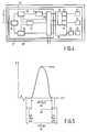
- Fig. 1 shows a peak value hold circuit 1 according to the invention, comprising a feedback loop 2 with a comparator element 3 which comparator element has a first input 4 for receiving an input signal U i and a second input 5 for receiving a feedback signal U f .
- An output 6 of the comparator element 3 applies a control signal U c to an input 7 of a digital hold element 8.
- An output 9 of the digital hold element 8 produces a digital output signal U0 which is also applied to an input of a D/A converter 11.
- An output 12 of the D/A converter 11 is coupled to the second input of the comparator element 3.
- the comparator element 3 produces the control signal U c , causing the voltage U0 on the output 9 of the digital hold element 8 to increase. If the input voltage U i is smaller than or equal to the feedback voltage U f , the output voltage U0 remains constant. In this manner the peak value of the input voltage U i is held in digital form for a specific period of time. If the (+)input and the (-)input of the comparator element 3 are reversed, a hold circuit 1 will be obtained that holds the minimum value of an input voltage (U i ).
- the digital hold element 8 is a counter 13, an enable input 14 of which forms the input 7 to the hold element 8 and an output 15 of which forms the output 9 of the hold element 8.
- the counter 13 continues counting, so that the output value U0 continues rising.
- the counter 13 continues counting, so that the output value U o continues rising.
- the counter stops counting and the output value U0 of the counter 13 remains constant.
- the counter 13 may be reset by a reset signal U r applied through the reset input 16.
- the hold element 8 may be arranged as a down counter 17.
- Fig. 2 the input voltage U i and the feedback voltage U f are plotted against time in the case where the hold circuit holds the peak value.
- the feedback voltage U f is the analog equivalent to the digital output voltage U0.
- the feedback voltage U f trails the input voltage U i until it exceeds the input voltage U i .
- the voltage U f then remains constant. Once the input voltage U i has exceeded the feedback voltage U f , the voltage U f in its turn trails the voltage U i .
- Fig. 3 shows a digital radio communication system 20 comprising a plurality of mobile stations MS1, MS2, MS3, MS4 and MS5, and a plurality of base stations BS1, BS2 and BS3. Each of these base stations BS1, BS2 and BS3 is coupled to an exchange 23 over respective data lines D1, D2 and D3.
- the control means 38 is coupled to a signal processing unit 39 which unit customarily comprises an A/D converter 40, a D/A converter 41 and a CODEC 42 for converting and (de)coding speech in digitized speech and vice versa .
- a microphone 43 and a loudspeaker or other acoustic converter 44 are coupled to the signal processing unit 39 and for the purpose of data, for example, a facsimile device 45 via a modem 46.
- the signals are transmitted to an exchange 23 over data lines D1, D2 or D3.
- Fig. 5 shows a time slot TS of the digital radio communication system 20 operating according to what is commonly referred to as the DECT standard (Digital European Cordless Telecommunications).
- the remaining period of time within a time slot is called guard space GS.
- a maximum value U max of the input signal U i is to be determined during the interval in which data are transferred, including a preceding period ES1 of 10 ⁇ s and a subsequent period ES2 of 10 ⁇ s. In the remaining time of a time slot the maximum value U max is read out and the counter 13 reset.
Landscapes
- Engineering & Computer Science (AREA)
- Physics & Mathematics (AREA)
- Electromagnetism (AREA)
- General Physics & Mathematics (AREA)
- Radar, Positioning & Navigation (AREA)
- Automation & Control Theory (AREA)
- Mobile Radio Communication Systems (AREA)
Priority Applications (1)
| Application Number | Priority Date | Filing Date | Title |
|---|---|---|---|
| EP19930203453 EP0602722A3 (fr) | 1992-12-14 | 1993-12-09 | Circuit de maintien station mobile, station de base et système de radiocommunication avec un tel circuit. |
Applications Claiming Priority (3)
| Application Number | Priority Date | Filing Date | Title |
|---|---|---|---|
| EP92203889 | 1992-12-14 | ||
| EP92203889 | 1992-12-14 | ||
| EP19930203453 EP0602722A3 (fr) | 1992-12-14 | 1993-12-09 | Circuit de maintien station mobile, station de base et système de radiocommunication avec un tel circuit. |
Publications (2)
| Publication Number | Publication Date |
|---|---|
| EP0602722A2 true EP0602722A2 (fr) | 1994-06-22 |
| EP0602722A3 EP0602722A3 (fr) | 1994-10-26 |
Family
ID=26131854
Family Applications (1)
| Application Number | Title | Priority Date | Filing Date |
|---|---|---|---|
| EP19930203453 Withdrawn EP0602722A3 (fr) | 1992-12-14 | 1993-12-09 | Circuit de maintien station mobile, station de base et système de radiocommunication avec un tel circuit. |
Country Status (1)
| Country | Link |
|---|---|
| EP (1) | EP0602722A3 (fr) |
Family Cites Families (1)
| Publication number | Priority date | Publication date | Assignee | Title |
|---|---|---|---|---|
| FR2595889B1 (fr) * | 1986-03-14 | 1988-05-06 | Havel Christophe | Dispositif de controle de puissance d'emission dans une station emettrice-receptrice de radiocommunication |
-
1993
- 1993-12-09 EP EP19930203453 patent/EP0602722A3/fr not_active Withdrawn
Also Published As
| Publication number | Publication date |
|---|---|
| EP0602722A3 (fr) | 1994-10-26 |
Similar Documents
| Publication | Publication Date | Title |
|---|---|---|
| CN1134104C (zh) | 改进蜂窝电话中发射机功率的测量动态范围的系统 | |
| US4137499A (en) | Signal strength measuring transceiver | |
| EP0683938B1 (fr) | Dispositif de generation de frequence s'utilisant avec des telephones sans fil numeriques | |
| GB9916904D0 (en) | Testing response of a radio transceiver | |
| US6720757B2 (en) | Variable gain received signal strength indicator | |
| US5794152A (en) | Cordless telephone | |
| EP0602722A2 (fr) | Circuit de maintien station mobile, station de base et système de radiocommunication avec un tel circuit | |
| US4063033A (en) | Signal quality evaluator | |
| US5247704A (en) | Burst mode transmitter/receiver unit | |
| EP0645921A1 (fr) | Appareil téléphonique sans fil | |
| JPH06215596A (ja) | ホールド回路並びにホールド回路を具える移動局、基地局及びディジタル無線通信システム | |
| KR19980051651A (ko) | 모뎀과 공중용 전화선간의 연결장치 | |
| KR100508971B1 (ko) | 무선가입자망 시스템의 멀티 채널형 단말장치 | |
| JP2806588B2 (ja) | 変復調装置 | |
| KR100189411B1 (ko) | 휴대용 무선 전화기와 키폰시스템간의 인터페이스회로 | |
| KR100540247B1 (ko) | 무선가입자망 단말기와 유선전화기간의 에코 현상 제거장치 | |
| KR19980058133A (ko) | 무선전화기의 본체와 연동되는 핸디부의 벨 음량 조절장치 | |
| US6212245B1 (en) | Communication apparatus | |
| JPH0715220Y2 (ja) | コードレス電話装置 | |
| KR100316901B1 (ko) | 무선 모뎀의 전원 공급장치 | |
| KR0120014B1 (ko) | 무선 전화기의 프리다이얼 장치 및 방법 | |
| KR920006207Y1 (ko) | 전화기의 자동수신 상태 전환회로 | |
| JPS58213537A (ja) | 簡易無線通信システムにおけるマルチ・チヤンネル・アクセス装置 | |
| KR970009143A (ko) | 전화원격조정용기기의 다중 접속 장치 및 방법 | |
| JPH04352545A (ja) | スピーカーホーン付電話装置 |
Legal Events
| Date | Code | Title | Description |
|---|---|---|---|
| PUAI | Public reference made under article 153(3) epc to a published international application that has entered the european phase |
Free format text: ORIGINAL CODE: 0009012 |
|
| AK | Designated contracting states |
Kind code of ref document: A2 Designated state(s): CH DE FR GB LI |
|
| RAP1 | Party data changed (applicant data changed or rights of an application transferred) |
Owner name: FASELEC A.G. Owner name: PHILIPS ELECTRONICS N.V. |
|
| PUAL | Search report despatched |
Free format text: ORIGINAL CODE: 0009013 |
|
| AK | Designated contracting states |
Kind code of ref document: A3 Designated state(s): CH DE FR GB LI |
|
| 18D | Application deemed to be withdrawn |
Effective date: 19940427 |