EP0602807A2 - Cachespeichersystem - Google Patents
Cachespeichersystem Download PDFInfo
- Publication number
- EP0602807A2 EP0602807A2 EP93309319A EP93309319A EP0602807A2 EP 0602807 A2 EP0602807 A2 EP 0602807A2 EP 93309319 A EP93309319 A EP 93309319A EP 93309319 A EP93309319 A EP 93309319A EP 0602807 A2 EP0602807 A2 EP 0602807A2
- Authority
- EP
- European Patent Office
- Prior art keywords
- memory
- cache
- burst
- address
- mode
- Prior art date
- Legal status (The legal status is an assumption and is not a legal conclusion. Google has not performed a legal analysis and makes no representation as to the accuracy of the status listed.)
- Withdrawn
Links
Images


Classifications
-
- G—PHYSICS
- G06—COMPUTING OR CALCULATING; COUNTING
- G06F—ELECTRIC DIGITAL DATA PROCESSING
- G06F12/00—Accessing, addressing or allocating within memory systems or architectures
- G06F12/02—Addressing or allocation; Relocation
- G06F12/08—Addressing or allocation; Relocation in hierarchically structured memory systems, e.g. virtual memory systems
- G06F12/0802—Addressing of a memory level in which the access to the desired data or data block requires associative addressing means, e.g. caches
- G06F12/0844—Multiple simultaneous or quasi-simultaneous cache accessing
- G06F12/0846—Cache with multiple tag or data arrays being simultaneously accessible
-
- G—PHYSICS
- G06—COMPUTING OR CALCULATING; COUNTING
- G06F—ELECTRIC DIGITAL DATA PROCESSING
- G06F12/00—Accessing, addressing or allocating within memory systems or architectures
- G06F12/02—Addressing or allocation; Relocation
- G06F12/08—Addressing or allocation; Relocation in hierarchically structured memory systems, e.g. virtual memory systems
- G06F12/0802—Addressing of a memory level in which the access to the desired data or data block requires associative addressing means, e.g. caches
- G06F12/0877—Cache access modes
- G06F12/0879—Burst mode
Definitions
- a computer system would ideally use very fast memory for all of its temporary storage needs. This would allow the Central Processing Unit (CPU) to operate at its designed speed, without the need to wait for slower memory devices. However, slower memory is often used because it is less expensive, consumes less power, and provides more storage in a given space than does very fast memory.
- CPU Central Processing Unit
- Cache memory systems take advantage of this characteristic by storing recently accessed data in a small amount of very fast memory, called cache memory. Data which is read from slower main memory is stored in the faster cache memory, so that if a program must subsequently use the same data, this data may be read from the cache memory.
- cache memory systems increase the apparent speed of memory accesses in computer systems.
- a cache memory system must keep track of main memory addresses for which the data is available in the cache. When data is available in the cache, the main memory access is aborted in favor of cache access. This is called a cache "hit.”
- the frequency of cache hits may be increased in many ways. One method is to use an algorithm for deciding which data to place in cache that is tailored to the particular computer application. Another method for increasing the frequency of hits is to use a larger cache memory.
- the optimum amount of cache memory in a computer system depends on many factors including the particular application, the target cost of the system, the hardware used in the system, and the relative costs of main and cache memory. Some systems may be optimized by using multiple smaller caches, rather than one large cache. For instance, multiple smaller caches may be mapped into non-contiguous blocks of memory.
- a cache system which utilizes multiple cache memories must avoid contention interference between the caches. Contention occurs when more than one cache responds to a memory address with a cache hit.
- burst-mode Another problem may occur when a CPU utilizes a "burst-mode" operation. Burst-mode operations are performed on data in a sequential series of memory locations. Rather than have the CPU execute a new instruction to address each individual memory location, burst-mode allows the CPU to execute a single instruction specifying a starting memory address, an operation to be performed, and the length of the memory block on which to perform the operation. This may cause special problems in a multiple cache system when the starting memory address for a burst-mode operation starts in one cache and is completed in a different cache.
- Circuitry in the individual cache memory implements the mapping function by permitting a range of addresses to be selected by the CPU, and then responding with the cache function only when an address within this range is placed on the main memory address bus.
- Circuitry in the cache which automatically steps through the memory addresses specified by the operation and decides whether these addresses correspond to the area mapped by the cache.
- FIG. 1 shows a multiprocessing system with a shared main memory 1 where each CPU 2 has its own cache memory 3.
- the cache memory 3 serves not only to increase the speed of memory accesses, but also to reduce the level of contention on the main memory bus 4 for access to main memory 1.
- a CPU 2 in this system can directly access only its local cache 3, and not a cache 5 attached to another CPU 6.
- FIG. 2(a) shows a multiprocessing system which embodies the present invention wherein CPU 10 has multiple cache memories 12 to 15.
- a four-cache system is shown for explanation purposes only; this disclosure encompasses similar multi-cache systems using any number of caches.
- FIG. 2(b) is a representation of how a multiple cache system with four caches 12 to 15 is mapped into four blocks 22 to 25 of main memory 20. Assuming that the four main memory blocks 22 to 25 are non-overlapping, the four caches 12 to 15 will also be non-overlapping.
- circuitry in cache 12 to cache 15 examines the physical address of the memory access request. If the physical address is within the mapped range for a particular cache, that cache examines its contents for a hit. Since the caches are non-overlapping, only one cache can respond to the memory request, eliminating contention between the caches.
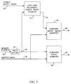
- FIG.3 is a block diagram of one embodiment of circuitry which prevents cache contention during initial and burst-mode memory accesses.
- a memory address 30 from the address bus passes through an input buffer 32 before being fed to the comparison circuitry.
- the buffered memory address 34 is compared with the mapped area 36 of the cache by comparator circuitry 38, producing a signal 39 when the buffered memory address 34 matches the mapped area 36 of the cache.
- Burst-mode operations send only the initial memory address 30, and not subsequent memory addresses.
- the subsequent memory addresses are generated by the burst circuitry 40 which latches and increments the buffered memory address 34.
- Burst circuitry 40 is enabled for the duration of the burst operation by burst-mode signal 42.
- Burst circuitry 40 generates a burst address 44 which is compared to the mapped area 36 of the cache by comparator circuitry 46, producing a signal 48 if the burst address 44 is within the mapped area 36 of the cache.
- burst circuitry 40 is disabled by burst-mode signal 42.
- Each cache is programmed with a unique mapped area 36 describing the physical address limits in which the cache operates.
- each cache employs a comparator circuit 38 to compare the memory address 30 to be accessed with the mapped area 36 for that cache. If the requested memory address 30 is within the range of addresses specified by the mapped area 36, then the circuitry proceeds with cache function. Otherwise, the circuitry does not respond to the memory request, so as not to interfere with any other cache which may respond to the memory request.
- a burst-mode operation may begin in one cache, but proceed into another cache.
- the burst-mode circuitry prevents cache contention.
- cache operation is enabled via signal 39.
- Subsequent burst addresses 44 which fall within the mapped area 36 will continue to enable cache operation via signal 48.
- subsequent burst addresses 44 are outside the mapped area 36 of the cache, the cache operation will be disabled via signal 48, preventing contention with another cache which may have the burst address 44 within its particular mapped area 36.
- One method of simplifying the circuit design of the comparator function 38 is to limit the scope of the mapped area 36 to an even power of two (i.e., 2, 4, 8... 1024, 2048... ), and require the mapped area 36 to start at an address which is either "0" or evenly divisible by the size of this mapped area.
- This implementation allows the comparator circuitry 38 to check only the higher-order bits of the buffered memory address 34 to determine whether it is within the range specified by the mapped area 36. This method may also be used by comparator circuitry 46.
- FIG. 4 An embodiment of the address comparison circuitry used in each cache is shown in FIG. 4. The implementation is shown for a system which allows up to 16 different caches, but the disclosure may be easily modified for other system requirements.
- the four high-order address bits 51 to 54 of the requested memory access are compared with the four map bits 61 to 64 which define the mapped area of the cache. If all of bits 51-54 equal bits 61-64, a high logic level "1" will be generated at the match output 70 of the circuitry. Otherwise the match output will remain low, or "0".
- the comparison circuit in FIG. 4 is composed of four comparator blocks 100, 110, 120, and 130. Each comparator block compares one bit of the requested address to one bit of the mapped area. For instance, address bit 51 is compared to map bit 61 in comparator block 110. If address bit 51 and map bit 61 are both "1", the output of AND gate 101 is “1" and the output 109 of OR gate 102 is “1". If address bit 51 and map bit 61 are both "0", inverters 103 and 104 will supply "1's" to the input of AND gate 105, causing a "1" to appear at the output 109 of OR gate 102. Therefore, the output 109 of comparator block 110 is “1” only if address bit 51 equals map bit 61.
- the output 119 of comparator block 110 is “1” only if address bit 52 equals map bit 62.
- the output 129 of comparator block 120 is “1” only if address bit 53 equals map bit 63.
- the output 139 of comparator block 130 is “1” only if address bit 54 equals map bit 64.
- the match output 70 of AND gate 140 is “1” only if address bits 51-54 equal map bits 61-64, causing each comparator block 100, 110, 120, and 130 to supply "1's" to the inputs 109, 119, 129, and 139 of the AND gate 140.
- each cache 12-15 contains the circuitry in FIG. 4.
- the caches 12-15 correspond to non-overlapping blocks 22-25 of main memory 20.
- at most one cache 12-15 can respond with a high match output 70 (in FIG. 4). Therefore, there can be no contention between caches 12-15 servicing a memory access request from CPU 10.
Landscapes
- Engineering & Computer Science (AREA)
- Theoretical Computer Science (AREA)
- Physics & Mathematics (AREA)
- General Engineering & Computer Science (AREA)
- General Physics & Mathematics (AREA)
- Memory System Of A Hierarchy Structure (AREA)
Applications Claiming Priority (2)
| Application Number | Priority Date | Filing Date | Title |
|---|---|---|---|
| US993005 | 1992-12-18 | ||
| US07/993,005 US5502828A (en) | 1992-12-18 | 1992-12-18 | Reducing memory access in a multi-cache multiprocessing environment with each cache mapped into different areas of main memory to avoid contention |
Publications (2)
| Publication Number | Publication Date |
|---|---|
| EP0602807A2 true EP0602807A2 (de) | 1994-06-22 |
| EP0602807A3 EP0602807A3 (de) | 1995-07-12 |
Family
ID=25538995
Family Applications (1)
| Application Number | Title | Priority Date | Filing Date |
|---|---|---|---|
| EP93309319A Withdrawn EP0602807A3 (de) | 1992-12-18 | 1993-11-23 | Cachespeichersystem. |
Country Status (3)
| Country | Link |
|---|---|
| US (2) | US5502828A (de) |
| EP (1) | EP0602807A3 (de) |
| JP (1) | JPH06222993A (de) |
Cited By (4)
| Publication number | Priority date | Publication date | Assignee | Title |
|---|---|---|---|---|
| WO1996039667A1 (en) * | 1995-06-05 | 1996-12-12 | Advanced Micro Devices, Inc. | Write cache for write performance improvement |
| EP0843261A3 (de) * | 1996-11-18 | 2000-02-23 | Nec Corporation | Speichersystem mit virtuellen Kanälen |
| WO2001029673A1 (de) * | 1999-10-22 | 2001-04-26 | Siemens Aktiengesellschaft | Speicherbaustein für ein mehrprozessorsystem und mehrprozessorsystem |
| US6708254B2 (en) | 1999-11-10 | 2004-03-16 | Nec Electronics America, Inc. | Parallel access virtual channel memory system |
Families Citing this family (13)
| Publication number | Priority date | Publication date | Assignee | Title |
|---|---|---|---|---|
| US6023466A (en) * | 1994-02-25 | 2000-02-08 | International Business Machines Corporation | Bit mapping apparatus and method |
| JP3153078B2 (ja) * | 1994-09-09 | 2001-04-03 | 日本電気株式会社 | データ処理装置 |
| US6728258B1 (en) * | 1995-11-15 | 2004-04-27 | Hitachi, Ltd. | Multi-processor system and its network |
| US5809537A (en) * | 1995-12-08 | 1998-09-15 | International Business Machines Corp. | Method and system for simultaneous processing of snoop and cache operations |
| US5901326A (en) * | 1996-11-26 | 1999-05-04 | International Business Machines Corporation | Memory bus address snooper logic for determining memory activity without performing memory accesses |
| US6606684B1 (en) * | 2000-03-31 | 2003-08-12 | Intel Corporation | Multi-tiered memory bank having different data buffer sizes with a programmable bank select |
| US6742071B1 (en) * | 2000-07-25 | 2004-05-25 | Cypress Semiconductor Corp. | Real-time I/O processor used to implement bus interface protocols |
| US8279886B2 (en) * | 2004-12-30 | 2012-10-02 | Intel Corporation | Dataport and methods thereof |
| US7562190B1 (en) | 2005-06-17 | 2009-07-14 | Sun Microsystems, Inc. | Cache protocol enhancements in a proximity communication-based off-chip cache memory architecture |
| US7444473B1 (en) | 2005-06-17 | 2008-10-28 | Sun Microsystems, Inc. | Speculative memory accesses in a proximity communication-based off-chip cache memory architecture |
| US7496712B1 (en) * | 2005-06-17 | 2009-02-24 | Sun Microsystems, Inc. | Proximity communication-based off-chip cache memory architectures |
| US8495299B2 (en) * | 2009-11-16 | 2013-07-23 | Microsoft Corporation | Non-blocking data transfer via memory cache manipulation |
| US10725689B2 (en) * | 2015-08-31 | 2020-07-28 | Hewlett Packard Enterprise Development Lp | Physical memory region backup of a volatile memory to a non-volatile memory |
Family Cites Families (6)
| Publication number | Priority date | Publication date | Assignee | Title |
|---|---|---|---|---|
| JPS58147879A (ja) * | 1982-02-26 | 1983-09-02 | Toshiba Corp | キヤツシユメモリ制御方式 |
| US4853846A (en) * | 1986-07-29 | 1989-08-01 | Intel Corporation | Bus expander with logic for virtualizing single cache control into dual channels with separate directories and prefetch for different processors |
| US5210843A (en) * | 1988-03-25 | 1993-05-11 | Northern Telecom Limited | Pseudo set-associative memory caching arrangement |
| JPH0748189B2 (ja) * | 1989-06-07 | 1995-05-24 | 三菱電機株式会社 | データ処理装置 |
| JPH04353947A (ja) * | 1991-02-13 | 1992-12-08 | Hewlett Packard Co <Hp> | メモリページ特性タグ付けシステム |
| US5398325A (en) * | 1992-05-07 | 1995-03-14 | Sun Microsystems, Inc. | Methods and apparatus for improving cache consistency using a single copy of a cache tag memory in multiple processor computer systems |
-
1992
- 1992-12-18 US US07/993,005 patent/US5502828A/en not_active Expired - Fee Related
-
1993
- 1993-11-23 EP EP93309319A patent/EP0602807A3/de not_active Withdrawn
- 1993-12-10 JP JP5310060A patent/JPH06222993A/ja active Pending
-
1995
- 1995-06-05 US US08/463,271 patent/US5737564A/en not_active Expired - Fee Related
Cited By (8)
| Publication number | Priority date | Publication date | Assignee | Title |
|---|---|---|---|---|
| WO1996039667A1 (en) * | 1995-06-05 | 1996-12-12 | Advanced Micro Devices, Inc. | Write cache for write performance improvement |
| US5761709A (en) * | 1995-06-05 | 1998-06-02 | Advanced Micro Devices, Inc. | Write cache for servicing write requests within a predetermined address range |
| EP0843261A3 (de) * | 1996-11-18 | 2000-02-23 | Nec Corporation | Speichersystem mit virtuellen Kanälen |
| US6167486A (en) * | 1996-11-18 | 2000-12-26 | Nec Electronics, Inc. | Parallel access virtual channel memory system with cacheable channels |
| US6327642B1 (en) | 1996-11-18 | 2001-12-04 | Nec Electronics, Inc. | Parallel access virtual channel memory system |
| US6477621B1 (en) | 1996-11-18 | 2002-11-05 | Nec Electronics, Inc. | Parallel access virtual channel memory system |
| WO2001029673A1 (de) * | 1999-10-22 | 2001-04-26 | Siemens Aktiengesellschaft | Speicherbaustein für ein mehrprozessorsystem und mehrprozessorsystem |
| US6708254B2 (en) | 1999-11-10 | 2004-03-16 | Nec Electronics America, Inc. | Parallel access virtual channel memory system |
Also Published As
| Publication number | Publication date |
|---|---|
| EP0602807A3 (de) | 1995-07-12 |
| US5502828A (en) | 1996-03-26 |
| JPH06222993A (ja) | 1994-08-12 |
| US5737564A (en) | 1998-04-07 |
Similar Documents
| Publication | Publication Date | Title |
|---|---|---|
| EP0602807A2 (de) | Cachespeichersystem | |
| US4803621A (en) | Memory access system | |
| US6226732B1 (en) | Memory system architecture | |
| US6910109B2 (en) | Tracking memory page state | |
| US5689679A (en) | Memory system and method for selective multi-level caching using a cache level code | |
| CA2020275C (en) | Apparatus and method for reading, writing, and refreshing memory with direct virtual or physical access | |
| EP0395559A2 (de) | Verteilter Cache-DRAM-Chip | |
| US4797813A (en) | Cache memory control apparatus | |
| EP0979456A1 (de) | Speicherzugangsschutz | |
| US5497458A (en) | Cache testability circuit for embedded diagnostics | |
| US6292867B1 (en) | Data processing system | |
| GB2335764A (en) | Selective caching of memory accesses based on access history | |
| EP0505157B1 (de) | Speicherzugriffssteuerung | |
| US20070294504A1 (en) | Virtual Address Cache And Method For Sharing Data Using A Unique Task Identifier | |
| JP3688736B2 (ja) | データメモリ | |
| JP2514292B2 (ja) | オペランドペ―ジメモリ及び命令ペ―ジメモリを有するコンピュ―タシステム | |
| KR100417548B1 (ko) | 집적된캐쉬메모리와,디지탈메모리에서메모리소자에데이타를제공하는방법 | |
| US5933856A (en) | System and method for processing of memory data and communication system comprising such system | |
| JPH0830568A (ja) | 分散メモリ型並列計算機のキャッシュ制御方式 | |
| JPH05313999A (ja) | メモリ制御装置 | |
| KR19990057856A (ko) | 저전력 캐쉬 메모리 장치 | |
| JPH0594376A (ja) | ポータブルコンピユータ | |
| KR100257750B1 (ko) | 메모리 겸용 캐시 | |
| KR0158487B1 (ko) | 반도체 메모리 캐쉬메모리 제어장치 및 그 방법 | |
| KR200182184Y1 (ko) | 메모리 겸용 캐시 |
Legal Events
| Date | Code | Title | Description |
|---|---|---|---|
| PUAI | Public reference made under article 153(3) epc to a published international application that has entered the european phase |
Free format text: ORIGINAL CODE: 0009012 |
|
| AK | Designated contracting states |
Kind code of ref document: A2 Designated state(s): BE DE DK ES FR GB GR IE IT LU NL PT SE |
|
| PUAL | Search report despatched |
Free format text: ORIGINAL CODE: 0009013 |
|
| AK | Designated contracting states |
Kind code of ref document: A3 Designated state(s): BE DE DK ES FR GB GR IE IT LU NL PT SE |
|
| 17P | Request for examination filed |
Effective date: 19951211 |
|
| 17Q | First examination report despatched |
Effective date: 19960806 |
|
| 18D | Application deemed to be withdrawn |
Effective date: 19970218 |