EP0602906A1 - Synchrone Vorrichtung und Verfahren für mehrere Prozessoren zur parallelen Ausführung mehrerer Programme - Google Patents
Synchrone Vorrichtung und Verfahren für mehrere Prozessoren zur parallelen Ausführung mehrerer Programme Download PDFInfo
- Publication number
- EP0602906A1 EP0602906A1 EP93309957A EP93309957A EP0602906A1 EP 0602906 A1 EP0602906 A1 EP 0602906A1 EP 93309957 A EP93309957 A EP 93309957A EP 93309957 A EP93309957 A EP 93309957A EP 0602906 A1 EP0602906 A1 EP 0602906A1
- Authority
- EP
- European Patent Office
- Prior art keywords
- synchronous
- status information
- processors
- processing
- register
- Prior art date
- Legal status (The legal status is an assumption and is not a legal conclusion. Google has not performed a legal analysis and makes no representation as to the accuracy of the status listed.)
- Granted
Links
Images


Classifications
-
- G—PHYSICS
- G06—COMPUTING OR CALCULATING; COUNTING
- G06F—ELECTRIC DIGITAL DATA PROCESSING
- G06F8/00—Arrangements for software engineering
- G06F8/40—Transformation of program code
- G06F8/41—Compilation
- G06F8/45—Exploiting coarse grain parallelism in compilation, i.e. parallelism between groups of instructions
- G06F8/458—Synchronisation, e.g. post-wait, barriers, locks
Definitions
- the present invention relates to a synchronous processing method and apparatus for a plurality of processors, and more particularly, to a method and apparatus in which a plurality of processors execute a plurality of programs in parallel and in synchronism.
- the synchronization combination storage element stores synchronization combination information indicating a combination of the processing elements to be synchronized per program for processing the program by the indicated plurality of processing elements.
- the synchronous status storage element stores synchronous status information showing that a synchronous waiting status is reached when that processing element finishes executing a process.
- the storage control element causes the synchronous status storage element to store the synchronous status information and simultaneously transmits the synchronous status information to all other processing elements.
- the synchronous receiving element receives the transmitted synchronous status information.
- the synchronous judging element judges, on the basis of the synchronization combination information stored in the synchronization combination storage element and the received synchronous status information, whether the processing elements are synchronized.
- the program process may be executed while each processing element becomes synchronized by transferring the status information between the plurality of processing elements.
- the processing elements are, e.g., processors the communication device is, e.g., a communication network.
- a selecting element for selecting any one of synchronous processing of a plurality of programs and synchronous processing of one program, which is to be performed by the plurality of synchronous status storage elements and by the plurality of synchronous judging elements.
- the selecting element may be a register controlled by the storage control element.
- the synchronous judging element may include a plurality of synchronous receiving elements for receiving the synchronous status information transmitted from all the processing elements and storing the received synchronous status information.
- the stored synchronization combination information indicates the combination of the processing elements to take the synchronization per program in order to process some programs by the plurality of processing elements.
- Stored subsequently may be the synchronous status information showing that the synchronous waiting status is reached when the self processing element has finished the processing.
- the synchronous status information is transmitted to all other processing elements.
- the synchronous status register 12 is accessed by the instruction processing element 8.
- the synchronous status register 12 is defined as a 1-bit length register for storing synchronous status information indicating that a synchronization waiting status for synchronization with another processor is reached, when the processor completes an execution of a program process.
- the synchronous status register 12 stores, e.g., a piece of synchronous status information "1", in accordance with the program when reaching the status to be synchronized with another processor by ending a program process.
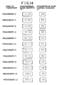
- the synchronous mask register 11, corresponding to synchronization combination storage element 11 of FIGURE 1, is accessed by the instruction processing element 8 and is an n-bit length register for storing synchronization combination information.
- n represents the number of processors.
- This synchronous mask register 11 stores, e.g., the synchronization combination information "1", with respect to other processors to be synchronized with its processor.
- the synchronous mask register 11, however, also stores synchronization combination information "0" with respect to other processors to not be synchronized with its processor.
- the processors 1-0, 1-1, 1-3, 1-4, 1-5 start executing processing k (step 102).
- k is initially 1, however, its value is incremented when repeating the process.
- the processors are at a status to take processor-to-processor synchronization on the program A.
- the instruction processing element 8 sets the synchronous status information of the synchronous status register 12 to "1" (step 103).
- the synchronous status information of the processors 1-0 ⁇ 1-(n-1) which has been inputted from the synchronous receiving element 15 is inputted to the corresponding OR circuits 81-0 ⁇ 81-(n-1).
- the synchronous status information of the processor 1-1 is inputted to the OR circuit 81-1 from the synchronous receiving element 15.
- the instruction processing element 8 monitors the synchronous indicating register 14 and judges whether or not 0 is set in the information of the synchronous indicating register 14 (step 113). Herein, if 0 is not set in the information of the synchronous indicating register 14, there is a waiting period until the information becomes 0 (step 114).
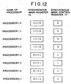
- processors 1-0 ⁇ 1-7 As illustrated in FIGURE 12, it is assumed that e.g., eight units of processors 1-0 ⁇ 1-7 are prepared. It is also presumed that the program A is executed by the processors 1-0, 1-1, 1-2, 1-3 in accordance with synchronization combination information "1110" among the processors 1-0, 1-1, 1-2, 1-3. The program B is executed by the processors 1-4, 1-5, 1-6, 1-7 in accordance with synchronization combination information "0111" among the processors 1-4, 1-5, 1-6, 1-7. Four-bit synchronous mask registers 16 are provided in the eight processors 1-0 ⁇ 1-7.
- step 209 when reaching a time required for taking the processor-to-processor synchronization, "0" is set in the synchronous status register 12 (step 209).
- the synchronous status information "0" of the synchronous status register 12 is transmitted to the synchronizing broadcasting element 22 in the network 2 (step 210).
- the synchronous status information "0" is broadcasted to all other processors from the synchronizing broadcasting element 22.
- the synchronous receiving elements 15 of the respective processors receive pieces of synchronous status information "0" of the synchronous status registers 12 of all other processors.
- the synchronous detecting element 13 executes the logic operation with respect to the synchronous status information of the synchronous receiving element 15 and the synchronous mask register 16, thereby detecting the synchronization (step 211).
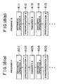
- the synchronous processing element 10c in the embodiment 3 includes synchronous status registers 12a and 12b, synchronous mask registers 11a and 11b, synchronous receiving elements 15a and 15b, synchronous detecting elements 13a and 13b and synchronous indicating registers 14a and 14b. Then, one group of elements and registers 11a, 12a, 13a, 14a, and 15a are employed for the synchronous processing of the program A, while the other group of elements and registers 11b, 12b, 13b, 14b, 15b are for the synchronous processing of the program B.
- the instruction processing element performs an arithmetic operation C1 of the subprogram C1 within one processor (step 421). Then, the synchronous processing element executes synchronization C1 (step 422). The data transfer element effects a transfer C1 of data of an arithmetic result to other processors (step 423). Further, the action proceeds to the next process, and steps 424, 425 are to be conducted.
- a parity generator 42 modifies the parity bit "1" of the data "110000011” from FF32 to "0", thereby generating data "110000010".
- This data "110000010” is inputted via FF33 to AND43.
- AND43 ANDs the data "110000001” stored in synchronous mask register 11 and the above data "110000010” and outputs the result to synchronous indicating register 14 via FF44, FF45.
- the data "110000001” from FF33 is identical with the data "110000001” from synchronous mask register 11, and hence the value of synchronous indicating register 14 changes from “0” to "1". Note that the value of synchronous indicating register 14 reversely changes from “1” to "0” as the case may be.
- AND 39 ANDs the data from FF36, the data from synchronous indicating register 14 and the data from FFs 47a ⁇ 47n through AND46. If the parity error is present, AND39 is turned ON and modifies instruction processing element 8 of the system-down information.
Landscapes
- Engineering & Computer Science (AREA)
- General Engineering & Computer Science (AREA)
- Theoretical Computer Science (AREA)
- Software Systems (AREA)
- Physics & Mathematics (AREA)
- General Physics & Mathematics (AREA)
- Multi Processors (AREA)
Applications Claiming Priority (3)
| Application Number | Priority Date | Filing Date | Title |
|---|---|---|---|
| JP33850292A JP3285629B2 (ja) | 1992-12-18 | 1992-12-18 | 同期処理方法及び同期処理装置 |
| JP33850292 | 1992-12-18 | ||
| JP338502/92 | 1992-12-18 |
Publications (2)
| Publication Number | Publication Date |
|---|---|
| EP0602906A1 true EP0602906A1 (de) | 1994-06-22 |
| EP0602906B1 EP0602906B1 (de) | 1999-06-09 |
Family
ID=18318765
Family Applications (1)
| Application Number | Title | Priority Date | Filing Date |
|---|---|---|---|
| EP93309957A Expired - Lifetime EP0602906B1 (de) | 1992-12-18 | 1993-12-10 | Synchrone Vorrichtung und Verfahren für mehrere Prozessoren zur parallelen Ausführung mehrerer Programme |
Country Status (4)
| Country | Link |
|---|---|
| US (1) | US5634071A (de) |
| EP (1) | EP0602906B1 (de) |
| JP (1) | JP3285629B2 (de) |
| DE (1) | DE69325246T2 (de) |
Cited By (7)
| Publication number | Priority date | Publication date | Assignee | Title |
|---|---|---|---|---|
| EP0544535A3 (de) * | 1991-11-28 | 1994-10-12 | Fujitsu Ltd | Paralleles Datenverarbeitungssteuerungssystem. |
| CN1070625C (zh) * | 1998-01-15 | 2001-09-05 | 英业达股份有限公司 | 一种网络对打应用程序中的同步控制方法 |
| US8489747B2 (en) | 2009-12-10 | 2013-07-16 | Royal Bank Of Canada | Synchronized processing of data by networked computing resources |
| US9940670B2 (en) | 2009-12-10 | 2018-04-10 | Royal Bank Of Canada | Synchronized processing of data by networked computing resources |
| US9959572B2 (en) | 2009-12-10 | 2018-05-01 | Royal Bank Of Canada | Coordinated processing of data by networked computing resources |
| US9979589B2 (en) | 2009-12-10 | 2018-05-22 | Royal Bank Of Canada | Coordinated processing of data by networked computing resources |
| US10057333B2 (en) | 2009-12-10 | 2018-08-21 | Royal Bank Of Canada | Coordinated processing of data by networked computing resources |
Families Citing this family (10)
| Publication number | Priority date | Publication date | Assignee | Title |
|---|---|---|---|---|
| JO1812B1 (en) † | 1993-10-15 | 1995-07-05 | ساسول كيميكال اندستريز ليمتد | Porous granules of ammonium nitrate |
| GB9606833D0 (en) * | 1996-03-30 | 1996-06-05 | Int Computers Ltd | Multi-processor system |
| US5958019A (en) * | 1996-07-01 | 1999-09-28 | Sun Microsystems, Inc. | Multiprocessing system configured to perform synchronization operations |
| US6067610A (en) * | 1996-07-29 | 2000-05-23 | Motorola, Inc. | Method and data processor for synchronizing multiple masters using multi-bit synchronization indicators |
| US6029204A (en) * | 1997-03-13 | 2000-02-22 | International Business Machines Corporation | Precise synchronization mechanism for SMP system buses using tagged snoop operations to avoid retries |
| US6314495B1 (en) * | 1998-01-07 | 2001-11-06 | International Business Machines Corporation | Method and apparatus for executing multiply-initiated, multiply-sourced variable delay system bus operations |
| JP2000132529A (ja) * | 1998-10-23 | 2000-05-12 | Sony Corp | 並列処理装置、並列処理方法および記録媒体 |
| KR100394827B1 (ko) * | 1999-12-22 | 2003-08-21 | 엘지전자 주식회사 | 이동통신교환기의 프로세서 재시동을 위한 프로그램 및데이터 적재방법 |
| JP5273045B2 (ja) | 2007-06-20 | 2013-08-28 | 富士通株式会社 | バリア同期方法、装置、及びプロセッサ |
| WO2012127534A1 (ja) * | 2011-03-23 | 2012-09-27 | 富士通株式会社 | バリア同期方法、バリア同期装置及び演算処理装置 |
Citations (2)
| Publication number | Priority date | Publication date | Assignee | Title |
|---|---|---|---|---|
| EP0473452A2 (de) * | 1990-08-31 | 1992-03-04 | Ncr Corporation | Mehrfachverarbeitungsfähige Arbeitsstation |
| EP0475282A2 (de) * | 1990-09-14 | 1992-03-18 | Hitachi, Ltd. | Synchrones Verfahren und Gerät für Prozessoren |
Family Cites Families (4)
| Publication number | Priority date | Publication date | Assignee | Title |
|---|---|---|---|---|
| US5243698A (en) * | 1982-11-26 | 1993-09-07 | Inmos Limited | Microcomputer |
| JPS6345670A (ja) * | 1986-08-13 | 1988-02-26 | Hitachi Ltd | プロセツサ間同期装置 |
| JP2594979B2 (ja) * | 1987-10-23 | 1997-03-26 | 株式会社日立製作所 | マルチプロセツサシステム |
| JPH0630094B2 (ja) * | 1989-03-13 | 1994-04-20 | インターナショナル・ビジネス・マシーンズ・コーポレイション | マルチプロセツサ・システム |
-
1992
- 1992-12-18 JP JP33850292A patent/JP3285629B2/ja not_active Expired - Fee Related
-
1993
- 1993-12-10 DE DE69325246T patent/DE69325246T2/de not_active Expired - Fee Related
- 1993-12-10 EP EP93309957A patent/EP0602906B1/de not_active Expired - Lifetime
-
1996
- 1996-02-15 US US08/601,705 patent/US5634071A/en not_active Expired - Lifetime
Patent Citations (2)
| Publication number | Priority date | Publication date | Assignee | Title |
|---|---|---|---|---|
| EP0473452A2 (de) * | 1990-08-31 | 1992-03-04 | Ncr Corporation | Mehrfachverarbeitungsfähige Arbeitsstation |
| EP0475282A2 (de) * | 1990-09-14 | 1992-03-18 | Hitachi, Ltd. | Synchrones Verfahren und Gerät für Prozessoren |
Non-Patent Citations (1)
| Title |
|---|
| "Low-cost device for contention-free barrier synchronization", IBM TECHNICAL DISCLOSURE BULLETIN., vol. 31, no. 11, April 1989 (1989-04-01), NEW YORK US, pages 382 - 389, XP000066528 * |
Cited By (16)
| Publication number | Priority date | Publication date | Assignee | Title |
|---|---|---|---|---|
| EP0544535A3 (de) * | 1991-11-28 | 1994-10-12 | Fujitsu Ltd | Paralleles Datenverarbeitungssteuerungssystem. |
| US5832261A (en) * | 1991-11-28 | 1998-11-03 | Fujitsu Limited | Barrier synchronizing mechanism for a parallel data processing control system |
| CN1070625C (zh) * | 1998-01-15 | 2001-09-05 | 英业达股份有限公司 | 一种网络对打应用程序中的同步控制方法 |
| US8489747B2 (en) | 2009-12-10 | 2013-07-16 | Royal Bank Of Canada | Synchronized processing of data by networked computing resources |
| US8984137B2 (en) | 2009-12-10 | 2015-03-17 | Royal Bank Of Canada | Synchronized processing of data by networked computing resources |
| US9940670B2 (en) | 2009-12-10 | 2018-04-10 | Royal Bank Of Canada | Synchronized processing of data by networked computing resources |
| US9959572B2 (en) | 2009-12-10 | 2018-05-01 | Royal Bank Of Canada | Coordinated processing of data by networked computing resources |
| US9979589B2 (en) | 2009-12-10 | 2018-05-22 | Royal Bank Of Canada | Coordinated processing of data by networked computing resources |
| US10057333B2 (en) | 2009-12-10 | 2018-08-21 | Royal Bank Of Canada | Coordinated processing of data by networked computing resources |
| US10650450B2 (en) | 2009-12-10 | 2020-05-12 | Royal Bank Of Canada | Synchronized processing of data by networked computing resources |
| US10664912B2 (en) | 2009-12-10 | 2020-05-26 | Royal Bank Of Canada | Synchronized processing of data by networked computing resources |
| US10706469B2 (en) | 2009-12-10 | 2020-07-07 | Royal Bank Of Canada | Synchronized processing of data by networked computing resources |
| US11308554B2 (en) | 2009-12-10 | 2022-04-19 | Royal Bank Of Canada | Synchronized processing of data by networked computing resources |
| US11308555B2 (en) | 2009-12-10 | 2022-04-19 | Royal Bank Of Canada | Synchronized processing of data by networked computing resources |
| US11776054B2 (en) | 2009-12-10 | 2023-10-03 | Royal Bank Of Canada | Synchronized processing of data by networked computing resources |
| US11823269B2 (en) | 2009-12-10 | 2023-11-21 | Royal Bank Of Canada | Synchronized processing of data by networked computing resources |
Also Published As
| Publication number | Publication date |
|---|---|
| US5634071A (en) | 1997-05-27 |
| DE69325246D1 (de) | 1999-07-15 |
| EP0602906B1 (de) | 1999-06-09 |
| JP3285629B2 (ja) | 2002-05-27 |
| JPH06187303A (ja) | 1994-07-08 |
| DE69325246T2 (de) | 1999-09-30 |
Similar Documents
| Publication | Publication Date | Title |
|---|---|---|
| US5634071A (en) | Synchronous processing method and apparatus for a plurality of processors executing a plurality of programs in parallel | |
| US5765009A (en) | Barrier synchronization system in parallel data processing | |
| US5781775A (en) | Parallel process scheduling method in a parallel computer and a processing apparatus for a parallel computer | |
| EP0460599B1 (de) | Massiv paralleler Rechner mit auf Schlangen basiertem Nachrichtenablieferungssystem | |
| US4507728A (en) | Data processing system for parallel processing of different instructions | |
| JP3617851B2 (ja) | パイプライン化データ処理方法 | |
| CN101739381B (zh) | 屏障同步设备、屏障同步系统以及屏障同步方法 | |
| JP2601591B2 (ja) | 並列計算機およびその全対全通信方法 | |
| EP0154051A1 (de) | Integrierter programmierbarer Prozessor für die wortweise Verarbeitung von digitalen Signalen | |
| EP0125044B1 (de) | Mikrocomputer mit Interprozesskommunikation | |
| US4956800A (en) | Arithmetic operation processing apparatus of the parallel processing type and compiler which is used in this apparatus | |
| EP0184791A1 (de) | Informationsverarbeitungsgerät zur schnellen Verarbeitung von Befehlen aus verschiedenen Gruppen | |
| JPH0668053A (ja) | 並列計算機 | |
| US5832261A (en) | Barrier synchronizing mechanism for a parallel data processing control system | |
| US20050086412A1 (en) | System and method for communicating between modules | |
| US5991866A (en) | Method and system for generating a program to facilitate rearrangement of address bits among addresses in a massively parallel processor system | |
| JPH11110362A (ja) | 計算機間データ通信方法 | |
| US4809171A (en) | Concurrent processing of data operands | |
| EP0105125B1 (de) | Datenverarbeitungssystem | |
| US11940940B2 (en) | External exchange connectivity | |
| JP2908202B2 (ja) | 論理シミュレータにおける同期装置と制御情報作成装置 | |
| EP0107447B1 (de) | Datenverteiler für Rechner | |
| KR19990074894A (ko) | 시리얼 버스라인을 이용한 데이터 전송장치 및방법 | |
| SU866560A1 (ru) | Устройство дл распределени за вок по процессорам | |
| EP0333306A2 (de) | Integrierter und programmierbarer Prozessor für die wortweise Verarbeitung von digitalen Signalen |
Legal Events
| Date | Code | Title | Description |
|---|---|---|---|
| PUAI | Public reference made under article 153(3) epc to a published international application that has entered the european phase |
Free format text: ORIGINAL CODE: 0009012 |
|
| AK | Designated contracting states |
Kind code of ref document: A1 Designated state(s): DE FR GB |
|
| 17P | Request for examination filed |
Effective date: 19940719 |
|
| 17Q | First examination report despatched |
Effective date: 19970917 |
|
| GRAG | Despatch of communication of intention to grant |
Free format text: ORIGINAL CODE: EPIDOS AGRA |
|
| GRAG | Despatch of communication of intention to grant |
Free format text: ORIGINAL CODE: EPIDOS AGRA |
|
| GRAH | Despatch of communication of intention to grant a patent |
Free format text: ORIGINAL CODE: EPIDOS IGRA |
|
| GRAH | Despatch of communication of intention to grant a patent |
Free format text: ORIGINAL CODE: EPIDOS IGRA |
|
| GRAA | (expected) grant |
Free format text: ORIGINAL CODE: 0009210 |
|
| AK | Designated contracting states |
Kind code of ref document: B1 Designated state(s): DE FR GB |
|
| REF | Corresponds to: |
Ref document number: 69325246 Country of ref document: DE Date of ref document: 19990715 |
|
| ET | Fr: translation filed | ||
| PLBE | No opposition filed within time limit |
Free format text: ORIGINAL CODE: 0009261 |
|
| STAA | Information on the status of an ep patent application or granted ep patent |
Free format text: STATUS: NO OPPOSITION FILED WITHIN TIME LIMIT |
|
| 26N | No opposition filed | ||
| REG | Reference to a national code |
Ref country code: GB Ref legal event code: IF02 |
|
| PGFP | Annual fee paid to national office [announced via postgrant information from national office to epo] |
Ref country code: GB Payment date: 20061206 Year of fee payment: 14 |
|
| PGFP | Annual fee paid to national office [announced via postgrant information from national office to epo] |
Ref country code: DE Payment date: 20061207 Year of fee payment: 14 |
|
| PGFP | Annual fee paid to national office [announced via postgrant information from national office to epo] |
Ref country code: FR Payment date: 20061208 Year of fee payment: 14 |
|
| GBPC | Gb: european patent ceased through non-payment of renewal fee |
Effective date: 20071210 |
|
| PG25 | Lapsed in a contracting state [announced via postgrant information from national office to epo] |
Ref country code: DE Free format text: LAPSE BECAUSE OF NON-PAYMENT OF DUE FEES Effective date: 20080701 |
|
| REG | Reference to a national code |
Ref country code: FR Ref legal event code: ST Effective date: 20081020 |
|
| PG25 | Lapsed in a contracting state [announced via postgrant information from national office to epo] |
Ref country code: GB Free format text: LAPSE BECAUSE OF NON-PAYMENT OF DUE FEES Effective date: 20071210 |
|
| PG25 | Lapsed in a contracting state [announced via postgrant information from national office to epo] |
Ref country code: FR Free format text: LAPSE BECAUSE OF NON-PAYMENT OF DUE FEES Effective date: 20071231 |