EP0602966B1 - Informationsaufzeichnungs- und/oder wiedergabegerät - Google Patents
Informationsaufzeichnungs- und/oder wiedergabegerät Download PDFInfo
- Publication number
- EP0602966B1 EP0602966B1 EP93310149A EP93310149A EP0602966B1 EP 0602966 B1 EP0602966 B1 EP 0602966B1 EP 93310149 A EP93310149 A EP 93310149A EP 93310149 A EP93310149 A EP 93310149A EP 0602966 B1 EP0602966 B1 EP 0602966B1
- Authority
- EP
- European Patent Office
- Prior art keywords
- recording
- data
- data train
- reproduction signal
- flag bit
- Prior art date
- Legal status (The legal status is an assumption and is not a legal conclusion. Google has not performed a legal analysis and makes no representation as to the accuracy of the status listed.)
- Expired - Lifetime
Links
- 238000000034 method Methods 0.000 claims description 17
- 238000006243 chemical reaction Methods 0.000 claims description 16
- 238000004519 manufacturing process Methods 0.000 claims description 3
- 238000010586 diagram Methods 0.000 description 4
- 238000012546 transfer Methods 0.000 description 4
- 238000001514 detection method Methods 0.000 description 3
- 238000012545 processing Methods 0.000 description 3
- 238000000605 extraction Methods 0.000 description 2
- 238000013459 approach Methods 0.000 description 1
- 230000005540 biological transmission Effects 0.000 description 1
- 238000007796 conventional method Methods 0.000 description 1
- 230000001186 cumulative effect Effects 0.000 description 1
- 230000005291 magnetic effect Effects 0.000 description 1
- 230000001360 synchronised effect Effects 0.000 description 1
- 238000013519 translation Methods 0.000 description 1
Images




Classifications
-
- H—ELECTRICITY
- H04—ELECTRIC COMMUNICATION TECHNIQUE
- H04L—TRANSMISSION OF DIGITAL INFORMATION, e.g. TELEGRAPHIC COMMUNICATION
- H04L25/00—Baseband systems
- H04L25/38—Synchronous or start-stop systems, e.g. for Baudot code
- H04L25/40—Transmitting circuits; Receiving circuits
- H04L25/49—Transmitting circuits; Receiving circuits using code conversion at the transmitter; using predistortion; using insertion of idle bits for obtaining a desired frequency spectrum; using three or more amplitude levels ; Baseband coding techniques specific to data transmission systems
- H04L25/497—Transmitting circuits; Receiving circuits using code conversion at the transmitter; using predistortion; using insertion of idle bits for obtaining a desired frequency spectrum; using three or more amplitude levels ; Baseband coding techniques specific to data transmission systems by correlative coding, e.g. partial response coding or echo modulation coding transmitters and receivers for partial response systems
-
- G—PHYSICS
- G11—INFORMATION STORAGE
- G11B—INFORMATION STORAGE BASED ON RELATIVE MOVEMENT BETWEEN RECORD CARRIER AND TRANSDUCER
- G11B20/00—Signal processing not specific to the method of recording or reproducing; Circuits therefor
- G11B20/10—Digital recording or reproducing
- G11B20/10009—Improvement or modification of read or write signals
-
- G—PHYSICS
- G11—INFORMATION STORAGE
- G11B—INFORMATION STORAGE BASED ON RELATIVE MOVEMENT BETWEEN RECORD CARRIER AND TRANSDUCER
- G11B20/00—Signal processing not specific to the method of recording or reproducing; Circuits therefor
- G11B20/10—Digital recording or reproducing
- G11B20/14—Digital recording or reproducing using self-clocking codes
- G11B20/1403—Digital recording or reproducing using self-clocking codes characterised by the use of two levels
- G11B20/1423—Code representation depending on subsequent bits, e.g. delay modulation, double density code, Miller code
- G11B20/1426—Code representation depending on subsequent bits, e.g. delay modulation, double density code, Miller code conversion to or from block codes or representations thereof
Definitions
- the present invention relates to an information recording/reproduction apparatus for reproducing an information as an (N+1)-value reproduction data train, and extracting a reproduction clock from the reproduction data train and, more particularly, to an information recording/reproduction apparatus for generating a reproduction signal by equalizing a partial response waveform.
- an original data train to be recorded is called input information
- a data train which is converted according to a predetermined code-conversion rule, and is to be input to a precoder or an NRZI converter is called an input data train
- NRZI-converted data to be actually recorded on a recording medium is called a recording data train
- a signal which is reproduced from the recording medium, and is subjected to waveform equalization is called a reproduction signal
- reproduction data obtained by binarizing the reproduction signal and detected as binary data by a reproduction clock is called reproduction data.
- FIG. 1 shows a recording data train.
- a recording data waveform shown in (b) of Fig. 1 is generated according to the recording data train, and is recorded as a recording signal on a recording medium.
- a reproduction signal waveform shown in (c) of Fig. 1 is obtained.
- the reproduction signal waveform is binarized by comparing it with the slice level V 0 , a reproduction data waveform shown in (d) of Fig. 1 is generated.
- (e) of Fig. 1 shows a reproduction clock, and a reproduction data train shown in (f) of Fig. 1 is detected using the reproduction clock.
- the reproduction clock is extracted under the PLL control using the reproduction data. Therefore, unless data bits "0" continuously appear in the recording data train, an edge is generated in the reproduction data, and the clock can be extracted from the reproduction data itself.
- the partial response is a technique for reproducing information without removing inter-code interference by defining inter-code interference caused by transfer characteristics of a recording/reproduction system of the information recording/reproduction apparatus to be convolution of information.
- FIG. 2 shows signal waveforms of the reproduction system for an isolated bit.
- (a) of Fig. 2 shows a recording data train
- (b) of Fig. 2 shows a recording data waveform which is recorded on a recording medium.
- the recorded information is reproduced, and waveform equalization is performed, so that a reproduction signal has a reproduction signal waveform shown in (c) of Fig. 2.
- the bit interval of transfer data is T b , and a reproduction signal for two bits becomes 1 with respect to 1-bit data "1" when viewed from the reproduction signal. More specifically, data "1" has 1 as an inter-code interference in the next bit.
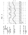
- Fig. 3 shows reproduction signal waveforms obtained when arbitrary data is recorded upon execution of such waveform equalization.
- (a) of Fig. 3 shows input data.
- a recording data train shown in (b) of Fig. 3 is obtained.
- (c) of Fig. 3 shows a recording data waveform of this recording data train, which waveform corresponds to a signal recorded on a recording medium.
- a reproduction signal shown in (d) of Fig. 3 is obtained.
- This reproduction signal is ternary-detected by level-slicing this signal by two slice levels V 1 and V 2 shown in (d) of Fig.
- PLL control is executed using a reproduction data signal obtained by comparing the reproduction signal with the slice level V 0 , as described above, thereby generating reproduction data synchronous with a reproduction clock. Therefore, the time interval required for the reproduction signal to cross the slice level, i.e., a change point of recording data from "1" to "0” or vice versa, e.g., as for NRZI codes, how many "0"s are present between two "1"s before NRZI conversion, determines the performance of codes in terms of controllability of PLL.
- the recording data train Z i becomes bit-reversed patterns depending on the flag bit "0" or “1", and depending on this conversion result, DSV (Digital Sum Variation: a difference between the total number of data bits "0" and the total number of data bits “1” of the recording data train) of the NRZI-converted recording data bit train is calculated.
- the flag bit "0" or “1” is then determined, so that the DSV approaches 0.
- a conventional reproduction detection means can extract a reproduction clock from reproduction data itself since data bits "0" do not continuously appear in recording data.
- the partial response is used, if input data includes continuous "1”s, since a recording data train also includes continuous "1”s, it is difficult to extract a reproduction clock from a reproduction signal for the above-mentioned reasons.
- EP-A-0143553 discloses a method of deriving a digital signal having a predetermined maximum number of consecutive digital zeros. This is achieved by dividing the digital signal into blocks which are then converted into an n-bit converted code including a number of primary combinations having a DC component substantially equal to zero when NRZI-coded, and a number of secondary combinations having a DC component having a value of two when NRZI-coded.
- a flag of value of either "0" or "1" is added to each block of data.
- the weight cumulative value DSV of the preceding block of data is calculated in order to select which flag is used.
- the present invention has been made in consideration of the above-mentioned problems, and has as its object to provide an information recording/reproduction apparatus and an information recording/reproduction method, which can extract a reproduction clock from a reproduction signal even when partial response waveform equalization is adopted.
- an apparatus for producing a recording data train for recording on a recording medium wherein information representative of the data is reproduced using partial response equalization in which the reproduction signal is read out from the recording medium as an (N+1)-value digital information signal, where N is an integer equal to or larger than 2, and the reproduction signal is compared with N slice levels;
- the apparatus being characterised by comprising means for adding a flag bit to each block of a predetermined number of binary data bits of an information data train; code conversion means for converting the information data train including the flag bits into a recording data train; and flag bit value means for causing the flag bit for each block to have a value such that the reproduction signal derived from the data bits in each block after recording information representative of the recording data train on a recording medium will cross at least one of the slice levels at least once within a predetermined period.
- a method for producing a recording data train for recording on an information recording medium wherein information representative of the recording data train is reproduced by partial response equalization in which the reproduction signal is compared with N slice levels, where N is an integer equal to or larger than 2, to generate a reproduction signal having N+1 digital levels, characterised by the steps of adding a flag bit to each block of a predetermined number of binary data bits of an information data train; converting the information data train including the flag bits into a recording data train; and causing the flag bit value for each block to be such that the reproduction signal derived from the data bits in each block after recording information representative of the recording data train on a recording medium will cross at least one of the slice levels at least once within a predetermined period.
- Fig. 5 is a block diagram showing an embodiment of an information recording/reproduction apparatus of the present invention.
- Fig. 5 illustrates only an arrangement of a recording data modulation processing system as main part of the present invention. Note that this embodiment adopts 8-9 NRZI conversion as a code conversion method.
- a flag bit adding circuit 1 adds a flag bit to input information sent from an external apparatus.
- input information is input in units of 8-bit blocks, and a 1-bit flag bit is added to the beginning of data of each block by the flag bit adding circuit 1.
- the flag bit to be added is fixed to be "0" in this embodiment.
- An NRZI converter 2 NRZI-converts output data from the flag bit adding circuit 1.
- a DSP determination circuit 3 detects a DC component (DSP; Disparity) of codes for one block in units of 8-bit blocks. More specifically, the DSP determination circuit 3 determines a difference between the numbers of data "1" and "0" in units of block data. If the number of "1"s is larger than the number of "0"s, the circuit 3 determines positive; otherwise, the circuit 3 determines negative.
- DSP DC component
- a flag bit reversing device 4 changes the flag bit added by the flag bit adding circuit 1 on the basis of determination results of the DSP determination circuit 3 and a DSV determination circuit 6 (to be described later). The arrangement of the bit reversing device 4 will be described in detail later.
- An NRZI converter 5 NRZI-converts output data from the flag bit reversing device 4 to generate recording data.
- the DSV determination circuit 6 detects a total DC component (DSV) of the recording data output from the NRZI converter 5. As described above, the DSV determination circuit 6 calculates a difference between the numbers of data bits "1" and "0" of a total recording data train.
- DSV total DC component
- the circuit 6 determines positive; if the number of "0"s is larger than the number of "1”s, the circuit 6 determines negative; and if the number of "0"s is equal to the number of "1"s, the circuit 6 determines 0.
- Fig. 6 is a block diagram showing the detailed circuit arrangement of the flag bit reversing device 4.
- the flag bit reversing device 4 comprises a 9-bit shift register 7, and a positive/negative determination circuit 8 for comparing the determination results from the DSP determination circuit 3 and the DSV determination circuit 6, and determining whether or not the two determination results coincide with each other, i.e., whether or not the two positive or negative determination results coincide with each other.
- the device 4 also comprises a 0 determination circuit 9 for detecting the determination result of 0 from the DSV determination circuit 6. More specifically, the DSV determination circuit 6 detects a difference between the numbers of data bits "1" and "0" of total data, and determines 0 if these numbers are equal to each other.
- the 0 determination circuit 9 also detects the DSV of 0.
- Input information is sequentially transferred to the flag bit adding circuit 1, and a flag bit "0" is added to the beginning of each 8-bit block data.
- the data added with the flag bit by the flag bit adding circuit 1 is supplied to the flag bit reversing device 4, and is transferred to the 9-bit shift register 7 in units of block data (8-bit data + 1-bit flag bit).
- data output from the flag bit adding circuit 1 is also supplied to the NRZI converter 2. After the data is NRZI-converted by the NRZI converter 2, the converted data is supplied to the DSP determination circuit 3.
- the DSP determination circuit 3 performs DSP determination by detecting the difference between the numbers of data bits "1" and "0" in units of block data, and outputs the determination result to the positive/negative determination circuit 8 of the flag bit reversing device 4.
- the positive/negative determination circuit 8 also receives the determination result from the DSV determination circuit 6. More specifically, the output data from the flag bit reversing device 4 is converted by the NRZI converter 5, and the converted data is output as a recording data train. In this case, the DSV determination circuit 6 detects the DSV of total data, as described above, and outputs the determination result to the positive/negative determination circuit 8. The determination result from the DSV determination circuit 6 is also output to the 0 determination circuit 9 in the flag bit reversing device 4.
- the positive/negative determination circuit 8 in the flag bit reversing device 4 resets the flip-flop to change the flag bit to "1".
- the positive/negative determination circuit 8 does not perform a resetting operation of the flip-flop, and hence, data with the flag bit "0" is supplied to the NRZI converter 5.
- the 0 determination circuit 9 monitors the determination result from the DSV determination circuit 6.
- the 0 determination circuit 9 maintains the flag bit to be 0. More specifically, in this case, the 0 determination circuit 9 supplies data with the flag bit "0" to the NRZI converter 5 independently of a coincidence or non-coincidence of the determination results from the DSP determination circuit 3 and the DSV determination circuit 6. In this manner, the flag bit of input data is changed in units of blocks based on the determination results from the DSP determination circuit 3 and the DSV determination circuit 6. Thereafter, NRZI conversion is performed, and the converted data is supplied as a recording data train to the next demodulation processing circuit.
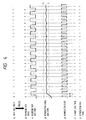
- Fig. 7 shows signal waveforms of the respective units obtained when the above-mentioned flag bit changing processing is performed.
- Fig. 7 exemplifies a case wherein data bits "1" continuously appear in input information.
- (a) of Fig. 7 shows output data from the flag bit reversing device 4.
- a bit "0" is inserted once per 18 bits since a flag bit is changed by the flag bit reversing device 4 based on the DSP and DSV determination results. Therefore, when this input data train is precoded, a recording data train shown in (b) of Fig. 7 is obtained, and furthermore, a recording data waveform shown in (c) of Fig.
- the flag bit when bits "1" continuously appear in an information data train over a predetermined period, the flag bit is set to be “0" on the basis of the DSP and DSV determination results, so that a bit "0" is inserted in the information data train at least once within the predetermined period.
- a reproduction signal can cross one of N slice levels at least once within the predetermined period.
- the above-mentioned embodiment exemplifies a case wherein bits "1" continuously appear in input information.
- the flag bit is changed, so that a bit "1" is inserted at least once within the predetermined period. Therefore, in this case as well, a reproduction signal crosses the slice level at least once within the predetermined period.
- the present invention allows extraction of a reproduction clock when the partial response is adopted, which extraction is difficult to achieve in the conventional method. Therefore, data reproduction by the self-clock system can be satisfactorily performed.
- the above embodiment exemplifies 8-9 NRZI codes.
- the present invention can be applied to other conversion rules such as 8-10 conversion.
Landscapes
- Engineering & Computer Science (AREA)
- Signal Processing (AREA)
- Physics & Mathematics (AREA)
- Spectroscopy & Molecular Physics (AREA)
- Computer Networks & Wireless Communication (AREA)
- Signal Processing For Digital Recording And Reproducing (AREA)
Claims (12)
- Gerät zur Erzeugung einer Aufzeichnungsdatenkette zur Aufzeichnung auf einem Aufzeichnungsträger, wobei die Daten darstellende Informationen unter Verwendung eines Teilantwort-Abgleichs wiedergegeben werden, bei dem das Wiedergabesignal von dem Aufzeichnungsträger als digitales (N+1)-Wert-Informationssignal ausgelesen wird, wobei N eine ganze Zahl größer oder gleich 2 ist, und das Wiedergabesignal mit N Grenzpegeln verglichen wird,
gekennzeichnet durcheine Einrichtung (1) zur Ergänzung eines Flagbits bei jedem Block einer vorbestimmten Anzahl von binären Datenbits einer Informationsdatenkette,eine Kode-Umwandlungseinrichtung (5) zur Umwandlung der die Flagbits aufweisenden Informationsdatenkette in eine Aufzeichnungsdatenkette sowieeine Flagbit-Werteinrichtung (4), die veranlaßt, daß das Flagbit für jeden Block einen derartigen Wert aufweist, daß das aus den Datenbits in jedem Block nach der Aufzeichnung von die Aufzeichnungsdatenkette darstellenden Informationen auf einem Aufzeichnungsträger hergeleitete Wiedergabesignal zumindest einen der Grenzpegel zumindest einmal in einer vorbestimmten Zeitdauer überschreitet. - Gerät nach Anspruch 1, miteiner DSP-Bestimmungseinrichtung (3) zur Erfassung der DC-Komponente jedes Blocks aus Datenbits undeiner DSV-Bestimmungseinrichtung (6) zur Erfassung der DC-Komponente der Aufzeichnungsdatenkette,wobei die Flagbit-Werteinrichtung (4) das Flagbit entsprechend den durch die DSP-Bestimmungseinrichtung (3) und die DSV-Bestimmungseinrichtung (6) erfaßten DC-Komponenten ändern kann.
- Gerät nach Anspruch 1 und 2, wobei der Aufzeichnungsträger ein magneto-optischer Aufzeichnungsträger ist.
- Gerät nach einem der vorhergehenden Ansprüche, wobei die Kode-Umwandlungseinrichtung (2) eine NRZI-Kode-Umwandlung ausführen kann.
- Aufzeichnungsgerät, das ein Gerät nach einem der vorhergehenden Ansprüche zur Erzeugung einer Datenkette sowie eine Einrichtung zur Aufzeichnung der Aufzeichnungsdatenkette auf einem Aufzeichnungsträger aufweist.
- System, das ein Aufzeichnungsgerät nach Anspruch 5 und eine Einrichtung zur Wiedergabe der Aufzeichnungsdatenkette unter Verwendung eines Teilantwort-Abgleichs aufweist, bei dem das Wiedergabesignal von dem Aufzeichnungsträger als digitales (N+1)-Wert-Informationssignal ausgelesen wird, wobei N eine ganze Zahl größer oder gleich 2 ist, und das Wiedergabesignal mit N Grenzpegeln verglichen wird.
- Verfahren zum Erzeugen einer Aufzeichnungsdatenkette zur Aufzeichnung auf einem Aufzeichnungsträger, wobei die Aufzeichnungsdatenkette darstellende Informationen durch einen Teilantwort-Abgleich wiedergegeben werden, bei dem das Wiedergabesignal mit N Grenzpegeln verglichen wird, wobei N eine ganze Zahl größer oder gleich 2 ist, damit ein Wiedergabesignal mit N+1 digitalen Pegeln erzeugt wird,
gekennzeichnet durch die SchritteErgänzen eines Flagbits bei jedem Block mit einer vorbestimmten Anzahl von binären Datenbits einer Informationsdatenkette,Umwandeln der die Flagbits aufweisenden Informationsdatenkette in eine Aufzeichnungsdatenkette sowieVeranlassen, daß das Flagbit für jeden Block einen derartigen Wert annimmt, daß das aus den Datenbits in jedem Block nach der Aufzeichnung von die Aufzeichnungsdatenkette darstellenden Informationen auf einem Aufzeichnungsträger hergeleitete Wiedergabesignal zumindest einen der Grenzpegel zumindest einmal in einer vorbestimmten Zeitdauer überschreitet. - Verfahren nach Anspruch 7 mit den SchrittenErfassen der DC-Komponente jedes Blocks aus Datenbits durch eine DSP-Bestimmungseinrichtung (3) undErfassen der DC-Komponente der Aufzeichnungsdatenkette durch eine DSV-Bestimmungseinrichtung (6),wobei der Veranlassungsschritt die Bestimmung des Flagbitwerts entsprechend den durch die DSP-Bestimmungseinrichtung (3) und die DSV-Bestimmungseinrichtung (6) erfaßten DC-Komponenten umfaßt.
- Verfahren nach Anspruch 7 oder 8, wobei der Aufzeichnungsträger ein magneto-optischer Aufzeichnungsträger ist.
- Verfahren nach einem der Ansprüche 7 bis 9, wobei die Kode-Umwandlung eine NRZI-Kode-Umwandlung ist.
- Aufzeichnungsverfahren, das ein Verfahren nach einem der Ansprüche 7 bis 10 zur Erzeugung einer Wiedergabedatenkette sowie den Schritt Aufzeichnen der Aufzeichnungsdatenkette auf einem Aufzeichnungsträger aufweist.
- Aufzeichnungs- und Wiedergabeverfahren mit einem Aufzeichnungsverfahren nach Anspruch 11 sowieeinem Schritt Wiedergeben der Aufzeichnungsdatenkette unter Verwendung eines Teilantwort-Abgleichs, bei dem das Wiedergabesignal von dem Aufzeichnungsträger als digitales (N+1)-Wert-Informationssignal ausgelesen wird, wobei N eine ganze Zahl größer oder gleich 2 ist, und das Wiedergabesignal mit N Grenzpegeln verglichen wird.
Applications Claiming Priority (3)
| Application Number | Priority Date | Filing Date | Title |
|---|---|---|---|
| JP4353876A JPH06187737A (ja) | 1992-12-16 | 1992-12-16 | 情報記録再生装置 |
| JP35387692 | 1992-12-16 | ||
| JP353876/92 | 1992-12-16 |
Publications (3)
| Publication Number | Publication Date |
|---|---|
| EP0602966A2 EP0602966A2 (de) | 1994-06-22 |
| EP0602966A3 EP0602966A3 (de) | 1995-02-15 |
| EP0602966B1 true EP0602966B1 (de) | 1999-06-09 |
Family
ID=18433824
Family Applications (1)
| Application Number | Title | Priority Date | Filing Date |
|---|---|---|---|
| EP93310149A Expired - Lifetime EP0602966B1 (de) | 1992-12-16 | 1993-12-15 | Informationsaufzeichnungs- und/oder wiedergabegerät |
Country Status (4)
| Country | Link |
|---|---|
| US (1) | US5548284A (de) |
| EP (1) | EP0602966B1 (de) |
| JP (1) | JPH06187737A (de) |
| DE (1) | DE69325247T2 (de) |
Families Citing this family (4)
| Publication number | Priority date | Publication date | Assignee | Title |
|---|---|---|---|---|
| JPH09128904A (ja) | 1995-11-01 | 1997-05-16 | Canon Inc | 情報再生装置 |
| US5786950A (en) * | 1996-07-29 | 1998-07-28 | Cirrus Logic, Inc. | PR4 sampled amplitude read channel employing an NRZI write modulator and a PR4/NRZI converter |
| TW341415U (en) * | 1997-04-08 | 1998-09-21 | United Microelectronics Corp | A digital data cutting circuit |
| TWI275254B (en) * | 2005-05-17 | 2007-03-01 | Cheertek Inc | Digital data slicing circuit and slicing method |
Family Cites Families (7)
| Publication number | Priority date | Publication date | Assignee | Title |
|---|---|---|---|---|
| US4408189A (en) * | 1981-05-18 | 1983-10-04 | Northern Telecom Limited | Method and apparatus for code conversion of binary to multilevel signals |
| JPS5994214A (ja) * | 1982-11-22 | 1984-05-30 | Hitachi Ltd | デイジタル信号記録装置 |
| JPH0683271B2 (ja) * | 1983-10-27 | 1994-10-19 | ソニー株式会社 | 情報変換方式 |
| JPH0775107B2 (ja) * | 1986-07-25 | 1995-08-09 | 株式会社日立製作所 | 磁気記録装置の信号再生回路 |
| EP0319216B1 (de) * | 1987-12-01 | 1994-07-27 | Matsushita Electric Industrial Co., Ltd. | Kodierungsgerät und dieses Gerät verwendendes magnetisches Aufzeichnungssystem |
| JP2664249B2 (ja) * | 1989-03-13 | 1997-10-15 | 株式会社日立製作所 | タイミング抽出回路,それを利用した通信システム及びタイミング抽出方法並びに通信装置 |
| JP2807362B2 (ja) * | 1991-09-30 | 1998-10-08 | 株式会社東芝 | 情報再生装置 |
-
1992
- 1992-12-16 JP JP4353876A patent/JPH06187737A/ja active Pending
-
1993
- 1993-12-14 US US08/165,847 patent/US5548284A/en not_active Expired - Lifetime
- 1993-12-15 EP EP93310149A patent/EP0602966B1/de not_active Expired - Lifetime
- 1993-12-15 DE DE69325247T patent/DE69325247T2/de not_active Expired - Lifetime
Also Published As
| Publication number | Publication date |
|---|---|
| EP0602966A3 (de) | 1995-02-15 |
| US5548284A (en) | 1996-08-20 |
| DE69325247T2 (de) | 1999-11-11 |
| JPH06187737A (ja) | 1994-07-08 |
| DE69325247D1 (de) | 1999-07-15 |
| EP0602966A2 (de) | 1994-06-22 |
Similar Documents
| Publication | Publication Date | Title |
|---|---|---|
| CN100557981C (zh) | 用于在有连续最小距离长度限制的情况下进行调制/解调的设备与方法 | |
| KR100263689B1 (ko) | 변조방법, 변조장치 및 복조장치 | |
| EP0673028B1 (de) | Aufzeichnungsmedium, Signalaufzeichnungsgerät dazu, und Signalwiedergabegerät dazu | |
| EP0144449B1 (de) | Verfahren und vorrichtung zum modulieren digitaler daten und zum demodulieren | |
| EP0143553B1 (de) | Verfahren und Gerät zur digitalen Datenkonversion | |
| JPH0544206B2 (de) | ||
| JPS5834002B2 (ja) | デイジタル信号の磁気記録再生方式 | |
| US5774286A (en) | Magnetic disk drive in which read data is demodulated using maximum likelihood detection method | |
| US4456905A (en) | Method and apparatus for encoding binary data | |
| JP3329185B2 (ja) | Rll符号化データの最大尤度シンボル検出 | |
| EP0902544A2 (de) | Modulator, Demodulator und Übertragungsträger | |
| US4672362A (en) | Binary data encoding and decoding process | |
| US4549167A (en) | Method of encoding and decoding binary data | |
| US5548284A (en) | Information recording and/or reproduction apparatus | |
| EP0090047B1 (de) | System zur kodierung und entkodierung binärer daten | |
| US20040257249A1 (en) | Method of converting a series of data words into a modulated signal | |
| EP0426034A2 (de) | Schaltung zur digitalen Modulation | |
| US4700241A (en) | Apparatus for recording and reproducing digital signals | |
| US5602547A (en) | Data conversion apparatus and encoding apparatus | |
| JP3239663B2 (ja) | 変調方法、変調装置及び復調装置 | |
| JPH0578110B2 (de) | ||
| KR20000004654A (ko) | 디지털 브이씨알의 등화기 | |
| JPS5994214A (ja) | デイジタル信号記録装置 | |
| KR0144965B1 (ko) | 이.에프.엠.(efm)복조의 에러정정방법 | |
| Tanaka et al. | Enhanced 8–10 Conversion Code for High Density Recording |
Legal Events
| Date | Code | Title | Description |
|---|---|---|---|
| PUAI | Public reference made under article 153(3) epc to a published international application that has entered the european phase |
Free format text: ORIGINAL CODE: 0009012 |
|
| AK | Designated contracting states |
Kind code of ref document: A2 Designated state(s): DE FR GB IT NL |
|
| PUAL | Search report despatched |
Free format text: ORIGINAL CODE: 0009013 |
|
| AK | Designated contracting states |
Kind code of ref document: A3 Designated state(s): DE FR GB IT NL |
|
| 17P | Request for examination filed |
Effective date: 19950630 |
|
| 17Q | First examination report despatched |
Effective date: 19970606 |
|
| GRAG | Despatch of communication of intention to grant |
Free format text: ORIGINAL CODE: EPIDOS AGRA |
|
| GRAG | Despatch of communication of intention to grant |
Free format text: ORIGINAL CODE: EPIDOS AGRA |
|
| GRAH | Despatch of communication of intention to grant a patent |
Free format text: ORIGINAL CODE: EPIDOS IGRA |
|
| GRAH | Despatch of communication of intention to grant a patent |
Free format text: ORIGINAL CODE: EPIDOS IGRA |
|
| GRAA | (expected) grant |
Free format text: ORIGINAL CODE: 0009210 |
|
| AK | Designated contracting states |
Kind code of ref document: B1 Designated state(s): DE FR GB IT NL |
|
| PG25 | Lapsed in a contracting state [announced via postgrant information from national office to epo] |
Ref country code: NL Free format text: LAPSE BECAUSE OF FAILURE TO SUBMIT A TRANSLATION OF THE DESCRIPTION OR TO PAY THE FEE WITHIN THE PRESCRIBED TIME-LIMIT Effective date: 19990609 Ref country code: IT Free format text: LAPSE BECAUSE OF FAILURE TO SUBMIT A TRANSLATION OF THE DESCRIPTION OR TO PAY THE FEE WITHIN THE PRE;WARNING: LAPSES OF ITALIAN PATENTS WITH EFFECTIVE DATE BEFORE 2007 MAY HAVE OCCURRED AT ANY TIME BEFORE 2007. THE CORRECT EFFECTIVE DATE MAY BE DIFFERENT FROM THE ONE RECORDED.SCRIBED TIME-LIMIT Effective date: 19990609 |
|
| REF | Corresponds to: |
Ref document number: 69325247 Country of ref document: DE Date of ref document: 19990715 |
|
| ET | Fr: translation filed | ||
| PLBE | No opposition filed within time limit |
Free format text: ORIGINAL CODE: 0009261 |
|
| STAA | Information on the status of an ep patent application or granted ep patent |
Free format text: STATUS: NO OPPOSITION FILED WITHIN TIME LIMIT |
|
| 26N | No opposition filed | ||
| REG | Reference to a national code |
Ref country code: GB Ref legal event code: IF02 |
|
| PGFP | Annual fee paid to national office [announced via postgrant information from national office to epo] |
Ref country code: FR Payment date: 20081222 Year of fee payment: 16 |
|
| REG | Reference to a national code |
Ref country code: FR Ref legal event code: ST Effective date: 20100831 |
|
| PG25 | Lapsed in a contracting state [announced via postgrant information from national office to epo] |
Ref country code: FR Free format text: LAPSE BECAUSE OF NON-PAYMENT OF DUE FEES Effective date: 20091231 |
|
| PGFP | Annual fee paid to national office [announced via postgrant information from national office to epo] |
Ref country code: GB Payment date: 20101223 Year of fee payment: 18 |
|
| PGFP | Annual fee paid to national office [announced via postgrant information from national office to epo] |
Ref country code: DE Payment date: 20101231 Year of fee payment: 18 |
|
| GBPC | Gb: european patent ceased through non-payment of renewal fee |
Effective date: 20121215 |
|
| REG | Reference to a national code |
Ref country code: DE Ref legal event code: R119 Ref document number: 69325247 Country of ref document: DE Effective date: 20130702 |
|
| PG25 | Lapsed in a contracting state [announced via postgrant information from national office to epo] |
Ref country code: DE Free format text: LAPSE BECAUSE OF NON-PAYMENT OF DUE FEES Effective date: 20130702 |
|
| PG25 | Lapsed in a contracting state [announced via postgrant information from national office to epo] |
Ref country code: GB Free format text: LAPSE BECAUSE OF NON-PAYMENT OF DUE FEES Effective date: 20121215 |